

查询LP2983供应商
LP2983
Micropower 150 mA Voltage Regulator in SOT-23
Package For Output Voltages ≤ 1.2V
Designed for Use with Very Low ESR Output Capacitors
LP2983 Micropower 150 mA Voltage Regulator in SOT-23 Package For Output Voltages ≤ 1.2V
October 2001
General Description
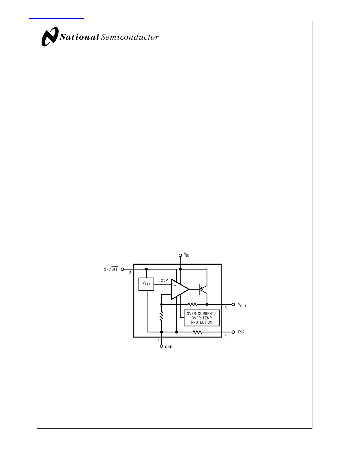
The LP2983 is a 150 mA, fixed-output voltage regulator
designed to provide tight voltage regulation in applications
with output voltages ≤ 1.2V.
Using an optimized VIP
cess, the LP2983 delivers unequalled performance in all
critical specifications:
Ground Pin Current: Typically 825 µA
@
75 µA
Enhanced Stability: The LP2983 is stable with output ca-
pacitor ESR down to zero, which allows the use of ceramic
capacitors on the output.
Smallest Possible Size: SOT-23 package uses absolute
minimum board space.
Precision Output: 1% tolerance output voltages available
(A grade).
1 mA load.
™
(Vertically Integrated PNP) pro-
@
150 mA load, and
Block Diagram
Features
n Guaranteed 150 mA output current
n Smallest possible size (SOT-23 package)
n Requires minimum external components
n Stable with low-ESR output capacitor
n Low ground pin current at all loads
n Output voltage accuracy 1% (A Grade)
n High peak current capability
n Wide supply voltage range (16V max)
n Low Z
n Overtemperature/overcurrent protection
n −40˚C to +125˚C junction temperature range
: 0.3Ω typical (10 Hz to 1 MHz)
OUT
Applications
n Cellular Phone
n Palmtop/Laptop Computer
n Personal Digital Assistant (PDA)
n Camcorder, Personal Stereo, Camera
20029101
VIP™is a trademark of National Semiconductor Corporation.
© 2001 National Semiconductor Corporation DS200291 www.national.com
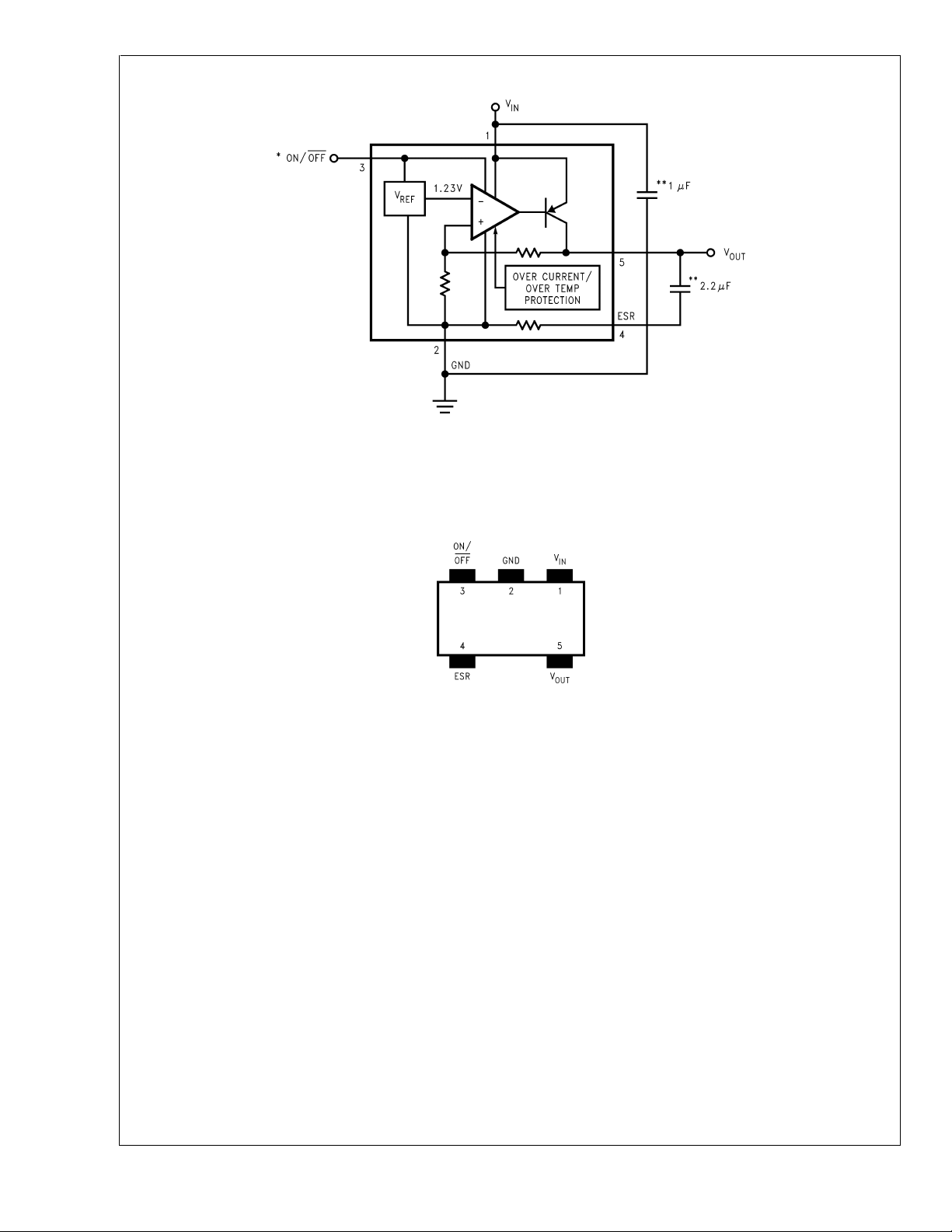
Basic Application Circuit
LP2983
*ON/OFF input must be actively terminated. Tie to VINif this function is not to be used.
**Minimum capacitance is shown to ensure stability (may be increased without limit). Ceramic capacitor required for output (see Application Hints).
20029102
Connection Diagram
5-Lead Small Outline Package (M5)
Top View
See NS Package Number MF05A
For ordering information see
20029103
Table 1
www.national.com 2
Ordering Information
TABLE 1. Package Marking and Ordering Information
Output Voltage
(V)
0.9 A LP2983AIM5X-0.9 LEJA 3000 Units on Tape and Reel
0.9 A LP2983AIM5-0.9 LEJA 1000 Units on Tape and Reel
0.9 STD LP2983IM5X-0.9 LEJB 3000 Units on Tape and Reel
0.9 STD LP2983IM5-0.9 LEJB 1000 Units on Tape and Reel
1.0 A LP2983AIM5X-1.0 LENA 3000 Units on Tape and Reel
1.0 A LP2983AIM5-1.0 LENA 1000 Units on Tape and Reel
1.0 STD LP2983IM5X-1.0 LENB 3000 Units on Tape and Reel
1.0 STD LP2983IM5-1.0 LENB 1000 Units on Tape and Reel
1.2 A LP2983AIM5X-1.2 LELA 3000 Units on Tape and Reel
1.2 A LP2983AIM5-1.2 LELA 1000 Units on Tape and Reel
1.2 STD LP2983IM5X-1.2 LELB 3000 Units on Tape and Reel
1.2 STD LP2983IM5-1.2 LELB 1000 Units on Tape and Reel
Grade Order Information
Package
Marking
Supplied as:
LP2983
www.national.com3

Absolute Maximum Ratings (Note 1)
If Military/Aerospace specified devices are required,
LP2983
please contact the National Semiconductor Sales Office/
Distributors for availability and specifications.
Storage Temperature Range −65˚C to +150˚C
Operating Junction Temperature
Range −40˚C to +125˚C
Lead Temp. (Soldering, 5 sec.) 260˚C
Power Dissipation (Note 3) Internally Limited
Input Supply Voltage (Survival) −0.3V to +16V
Input Supply Voltage (Operating) 2.2V to +16V
Shutdown Input Voltage (Survival) −0.3V to +16V
Output Voltage Survival, (Note 4) −0.3V to +9V
I
(Survival) Short Circuit
OUT
Input-Output Voltage Survival,(Note 5) −0.3V to +16V
ESD Rating (Note 2) 2 kV
Electrical Characteristics
Limits in standard typeface are for TJ= 25˚C. and limits in boldface type apply over the full operating temperature range. Unless otherwise specified: V
Symbol Parameter Conditions Typ
∆V
O
Output Voltage
Tolerance
Output Voltage VO(NOM)+1V ≤ VIN≤ 16V 0.01 0.016 0.016
Line Regulation 0.032 0.032
I
GND
V
(min) Minimum VINrequired
IN
Ground Pin Current IL= 0 65 95 95
to maintain Output
Regulation
V
ON/OFF
ON/OFF Input Voltage
(Note 7)
I
ON/OFF
e
n
ON/OFF Input Current V
Output Noise BW = 10 Hz to 100 kHz,
Voltage (RMS) C
Ripple Rejection f=1kHz
(SC) Short Circuit Current RL= 0 (Steady State)
I
O
I
(PK) Peak Output Current V
O
(NOM) + 1V, IL= 1 mA, CIN= 1 µF, C
IN=VO
1mA≤I
1mA≤I
I
= 1 mA 75 110 110
L
I
= 10 mA 120 220 220
L
I
= 50 mA 300 500 500
L
I
= 150 mA 825 1200 1500
L
V
ON/OFF
V
ON/OFF
≤50 mA −2.0 2.0 −2.5 2.5
L
≤150 mA −2.5 2.5 −3.0 3.0
L
<
0.15V 6 12 12
<
0.05V 0.2 2 2
High = O/P ON 1.4 1.6 1.6
Low = O/P OFF 0.1 0.05 0.05
= 0 0.01 −2 −2
ON/OFF
V
V
C
=5V 5 15 15
ON/OFF
=10µF 60 µV
OUT
= 1.2V
OUT
= 2.2 µF
OUT
≥ Vo(NOM) −5% 250
OUT
= 2.2 µF, V
OUT
ON/OFF
= 2V.
LP2983AI-X.X LP2983I-X.X
Min Max Min Max
−1.0 1.0 −1.5 1.5
−2.5 2.5 −3.5 3.5
−3.5 3.5 −4.0 4.0
125 125
170 170
400 400
900 900
2000 2000
2.05 2.20 2.20
65 dB
400
Protected
Units(Note 6) (Note 6)
%
%/V
µA
V
µA
mA(Note 8)
www.national.com 4

Electrical Characteristics (Continued)
Note 1: “Absolute Maximum Ratings” indicate limits beyond which damage to the component may occur. Electrical specifications do not apply when operating the
device outside of its rated operating conditions.
Note 2: The ESD rating of pin 3 is 1 kV.
Note 3: The maximum allowable power dissipation is a function of the maximum junction temperature, T
and the ambient temperature, T
. The maximum allowable power dissipation at any ambient temperture is calculated using:
A
(MAX), the junction-to-ambient thermal resistance, θ
J
J-A
LP2983
,
Where the value of θ
temperature, and the regulator will go into thermal shutdown.
Note 4: If used in a dual-supply system where the regulator load is returned to a negative supply, the LP2983 output must be diode-clamped to ground.
Note 5: The output PNP structure contains a diode between the V
turn on this diode and possibly cause a destructive latch-up condition (see Application Hints).
Note 6: Limits are 100% production tested at 25˚C. Limits over the operating temperature range are guaranteed through correlation using Statistical Quality Control
(SQC) methods. The limits are used to calculate National’s Average Outgoing Quality Level (AOQL).
Note 7: The ON/OFF input must be properly driven to prevent possible misoperation. For details, refer to Application Hints.
Note 8: The LP2983 has foldback current limiting which allows a high peak current when V
forced down to ground (see Typical Performance Characteristics curves).
for the SOT-23package is 240˚C/W in a typical PC board mounting. Exceeding the maximum allowable dissipation will cause excessive die
J-A
to V
IN
terminals that is normally reverse-biased. Reversing the polarity from VINto V
OUT
>
0.5V,and then reduces the maximum output current as V
OUT
OUT
will
OUT
is
www.national.com5

Typical Performance Characteristics Unless otherwise specified: C
V
(NOM) +1, TA= 25˚C, ON/OFF pin is tied to VIN.
OUT
LP2983
LP2983 Tempco Minimum Input Voltage vs Temperature
20029107 20029108
Input Current vs VIN(0mA Load) Input Current vs VIN(1mA Load)
= 1µF, C
IN
= 2.2µF, VIN=
OUT
20029109 20029110
Input Current vs VIN(50mA & 150mA Loads) GND Pin vs Load Current
20029111
20029112
www.national.com 6

LP2983
Typical Performance Characteristics Unless otherwise specified: C
V
(NOM) +1, TA= 25˚C, ON/OFF pin is tied to VIN. (Continued)
OUT
Line Transient Response
GND Pin vs Temperature and Load
20029113
Line Transient Response
∆V
= 1V, Load = 150mA
IN
∆V
= 1V, Load = 1mA
IN
Line Transient Response
∆VIN= 13.8V, Load = 1mA
= 1µF, C
IN
= 2.2µF, VIN=
OUT
20029114
20029115
Line Transient Response
∆V
= 13.8V, Load = 150mA Noise Density
IN
20029117
20029116
20029118
www.national.com7
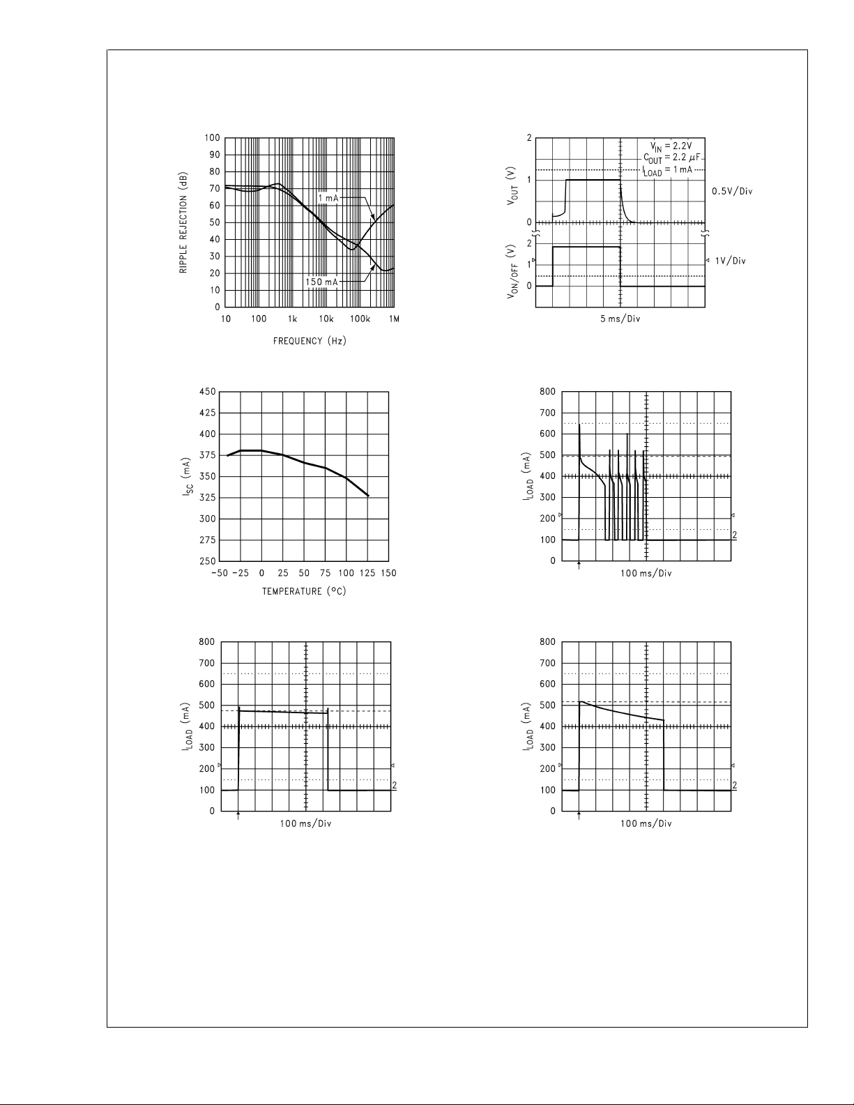
Typical Performance Characteristics Unless otherwise specified: C
V
(NOM) +1, TA= 25˚C, ON/OFF pin is tied to VIN. (Continued)
OUT
LP2983
= 1µF, C
IN
= 2.2µF, VIN=
OUT
Ripple Rejection C
= 2.2µF Turn-On Time
OUT
20029119
Short Circuit Current vs Temperature Short Circuit Current, VIN= 16V
20029121
20029122
20029127
Short Circuit Current, VIN= 2.8V Short Circuit Current, VIN=6V
20029123 20029124
www.national.com 8

LP2983
Typical Performance Characteristics Unless otherwise specified: C
V
(NOM) +1, TA= 25˚C, ON/OFF pin is tied to VIN. (Continued)
OUT
Load Transient Response
C
= 4.7µF
OUT
20029125 20029126
Load Transient Response
C
OUT
= 1µF, C
IN
= 2.2µF
= 2.2µF, VIN=
OUT
www.national.com9

Application Hints
LP2983
EXTERNAL CAPACITORS
Like any low-dropout regulator, the LP2983 requires external
capacitors for regulator stability. These capacitors must be
correctly selected for good performance.
Input Capacitor
An input capacitor whose capacitance is ≥ 1 µF is required
between the LP2983 input and ground (the amount of capacitance may be increased without limit).
This capacitor must be located a distance of not more than 1
cm from the input pin and returned to a clean analog ground.
Any good quality ceramic, tantalum, or film capacitor may be
used at the input.
Important: Tantalum capacitors can suffer catastrophic failure due to surge current when connected to a
low-impedance source of power (like a battery or very large
capacitor). If a Tantalum capacitor is used at the input, it
must be guaranteed by the manufacturer to have a surge
current rating sufficient for the application.
There are no requirements for ESR on the input capacitor,
but tolerance and temperature coefficient must be considered when selecting the capacitor to ensurethe capacitance
will be ≥ 1 µF over the entire operating temperature range.
Output Capacitor
The LP2983 is designed specifically to work with ceramic
output capacitors, utilizing circuitry which allows the regulator to be stable across the entire range of output current with
an output capacitor whose ESR is as low as zero ohms. See
Figure 1
below.
= 2.2µF
C
OUT
Ceramic to ESR Pin
ceramic capacitors can exhibit large changes incapacitance
with temperature (see next section,
tics
).
Capacitor Characteris-
The output capacitor must be located not more than 1 cm
from the output pin and returned to a clean analog ground.
CAPACITOR CHARACTERISTICS
The LP2983 was designed to work with ceramic capacitors
on the output to take advantage of the benefits they offer: for
capacitance values in the 2.2 µF to 4.7 µF range, ceramics
are the least expensive and also have the lowest ESR
values (which makes them best for eliminating
high-frequency noise).
One disadvantage of ceramic capacitors is that their capacitance can vary with temperature. Most large value ceramic
capacitors (≥ 2.2 µF) are manufactured with the Z5U orY5V
temperature characteristic, which results in the capacitance
dropping by more than 50% as the temperature goes from
25˚C to 85˚C.
This could cause problems if a 2.2 µF capacitor were used
on the output since it will drop down to approximately 1 µF at
high ambient temperatures (which could cause the LP2983
to oscillate). If Z5U orY5V capacitors are used on the output,
a minimum capacitance value of 4.7 µF must be observed.
Abetter choice for temperature coefficient in ceramic capacitors is X7R, which holds the capacitance within
±
15%. Unfortunately, the larger values of capacitance are not offered
by all manufacturers in the X7R dielectric.
ON/OFF INPUT OPERATION
The LP2983 is shut off by driving the ON/OFF input low, and
turned on by pulling it high. If this feature is not to be used,
the ON/OFF input should be tied to V
to keep the regulator
IN
output on at all times.
To assure proper operation, the signal source used to drive
the ON/OFF input must be able to swing above and below
the specified turn-on/turn-off voltage thresholds listed in the
Electrical Characteristics section under V
ON/OFF
. To prevent
mis-operation, the turn-on (and turn-off) voltage signals applied to the ON/OFF input must have a slew rate which is
≥ 40 mV/µs.
Caution: the regulator output voltage can not be guaranteed
if a slow-moving AC (or DC) signal is applied that is in the
range between the specified turn-on and turn-off voltages
listed under the electrical specification V
ON/OFF
(see Electrical Characteristics).
20029120
FIGURE 1.
The LP2983 requires a minimum of 2.2 µF on the output
(output capacitor size can be increased without limit).
It is important to remember that capacitor tolerance and
variation with temperature must be taken into consideration
when selecting an output capacitor so that the minimum
required amount of output capacitance is provided over the
full operating temperature range. It should be noted that
www.national.com 10
REVERSE INPUT-OUTPUT VOLTAGE
The PNP power transistor used as the pass element in the
LP2983 has an inherent diode connected between the regulator output and input. During normal operation (where the
input voltage is higher than the output) this diode is
reverse-biased.
However, if the output is pulled above the input, this diode
will turn ON and current will flow into the regulator output. In
such cases, a parasitic SCR can latch which will allow a high
current to flow into V
(and out the ground pin), which can
IN
damage the part.
In any application where the output may be pulled abovethe
input, an external Schottky diode must be connected from
V
to V
IN
(cathode on VIN, anode on V
OUT
), to limit the
OUT
reverse voltage across the LP2983 to 0.3V (see Absolute
Maximum Ratings).

Physical Dimensions inches (millimeters)
unless otherwise noted
LP2983 Micropower 150 mA Voltage Regulator in SOT-23 Package For Output Voltages ≤ 1.2V
5-Lead Small Outline Package (M5)
NS Package Number MF05A
For Order Numbers, refer to
Table 1
in the “Ordering Information” section of this document.
LIFE SUPPORT POLICY
NATIONAL’S PRODUCTS ARE NOT AUTHORIZED FOR USE AS CRITICAL COMPONENTS IN LIFE SUPPORT
DEVICES OR SYSTEMS WITHOUT THE EXPRESS WRITTEN APPROVAL OF THE PRESIDENT AND GENERAL
COUNSEL OF NATIONAL SEMICONDUCTOR CORPORATION. As used herein:
1. Life support devices or systems are devices or
systems which, (a) are intended for surgical implant
into the body, or (b) support or sustain life, and
whose failure to perform when properly used in
accordance with instructions for use provided in the
2. A critical component is any component of a life
support device or system whose failure to perform
can be reasonably expected to cause the failure of
the life support device or system, or to affect its
safety or effectiveness.
labeling, can be reasonably expected to result in a
significant injury to the user.
National Semiconductor
Corporation
Americas
Email: support@nsc.com
www.national.com
National Semiconductor
Europe
Fax: +49 (0) 180-530 85 86
Email: europe.support@nsc.com
Deutsch Tel: +49 (0) 69 9508 6208
English Tel: +44 (0) 870 24 0 2171
Français Tel: +33 (0) 1 41 91 8790
National Semiconductor
Asia Pacific Customer
Response Group
Tel: 65-2544466
Fax: 65-2504466
Email: ap.support@nsc.com
National Semiconductor
Japan Ltd.
Tel: 81-3-5639-7560
Fax: 81-3-5639-7507
National does not assume any responsibility for use of any circuitry described, no circuit patent licenses are implied and National reserves the right at any time without notice to change said circuitry and specifications.
 Loading...