


April 17, 2008
LMX2531
High Performance Frequency Synthesizer System with
Integrated VCO
LMX2531 High Performance Frequency Synthesizer System with Integrated VCO
General Description
The LMX2531 is a low power, high performance frequency
synthesizer system which includes a fully integrated deltasigma PLL and VCO with fully integrated tank circuit. The third
and fourth poles are also integrated and also adjustable. Also
included are integrated ultra-low noise and high precision
LDOs for the PLL and VCO which give higher supply noise
immunity and also more consistent performance. When combined with a high quality reference oscillator, the LMX2531
generates very stable, low noise local oscillator signals for up
and down conversion in wireless communication devices.
The LMX2531 is a monolithic integrated circuit, fabricated in
an advanced BiCMOS process. There are several different
versions of this product in order to accomodate different frequency bands.
Device programming is facilitated using a three-wire
MICROWIRE Interface that can operate down to 1.8 volts.
Supply voltage range is 2.8 to 3.2 Volts. The LMX2531 is
available in a 36 pin 6x6x0.8 mm Lead-Free Leadless Leadframe Package (LLP).
Target Applications
3G Cellular Base Stations (WCDMA, TD-
■
SCDMA,CDMA2000)
2G Cellular Base Stations (GSM/GPRS, EDGE,
■
CDMA1xRTT)
Wireless LAN
■
Broadband Wireless Access
■
Satellite Communications
■
Wireless Radio
■
Automotive
■
CATV Equipment
■
Instrumentation and Test Equipment
■
RFID Readers
■
Features
Multiple Frequency Options Available
■
See Selection Guide Below
—
Frequencies from: 553 MHz - 2790 MHz
—
PLL Features
■
Fractional-N Delta Sigma Modulator Order
—
programmable up to 4th order
FastLock/Cycle Slip Reduction with Timeout Counter
—
Partially integrated, adjustable Loop Filter
—
Very low phase noise and spurs
—
VCO Features
■
Integrated tank inductor
—
Low phase noise
—
Other Features
■
2.8 V to 3.2 V Operation
—
Low Power-Down Current
—
1.8V MICROWIRE Support
—
Package: 36 Lead LLP
—
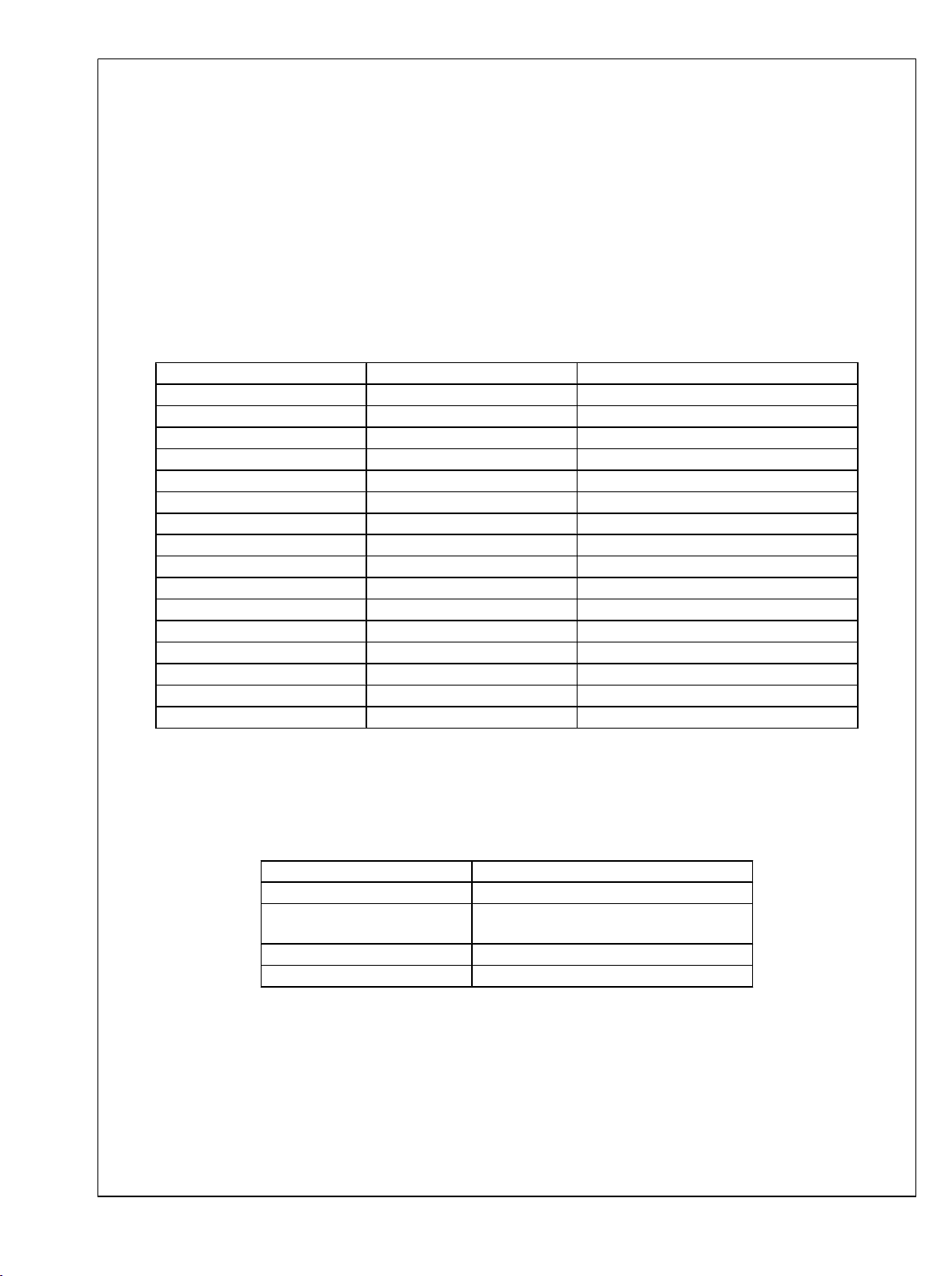
Part Low Band High Band
LMX2531LQ1146E 553 - 592 MHz 1106 - 1184 MHz
LMX2531LQ1226E 592 - 634 MHz 1184 - 1268 MHz
LMX2531LQ1312E 634 - 680 MHz 1268 - 1360 MHz
LMX2531LQ1415E 680 - 735 MHz 1360 - 1470 MHz
LMX2531LQ1515E 725 - 790 MHz 1450 - 1580 MHz
LMX2531LQ1570E 765 - 818 MHz 1530 - 1636 MHz
LMX2531LQ1650E 795 - 850 MHz 1590 - 1700 MHz
LMX2531LQ1700E 831 - 885 MHz 1662 - 1770 MHz
LMX2531LQ1742 880 - 933 MHz 1760 - 1866 MHz
LMX2531LQ1778E 863 - 920 MHz 1726 - 1840 MHz
LMX2531LQ1910E 917 - 1014 MHz 1834 - 2028 MHz
LMX2531LQ2080E 952 - 1137 MHz 1904 - 2274 MHz
LMX2531LQ2265E 1089 - 1200 MHz 2178 - 2400 MHz
LMX2531LQ2570E 1168 - 1395 MHz 2336 - 2790 MHz
© 2008 National Semiconductor Corporation 201011 www.national.com

Functional Block Diagram
LMX2531
20101101
www.national.com 2
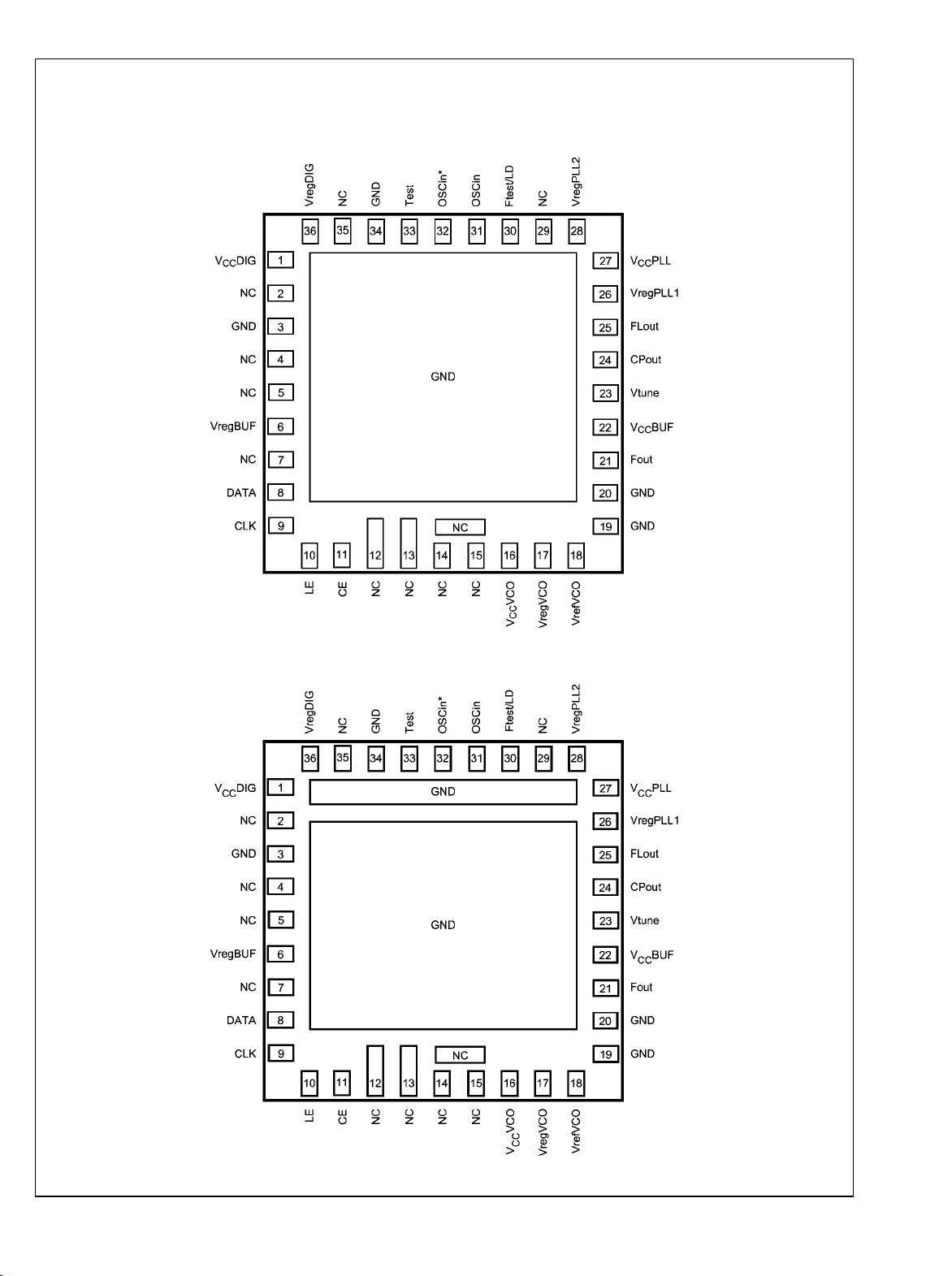
Connection Diagrams
LMX2531
36-Pin LLP (LQ) Package, D Version
(LMX2531LQ1146E/1226E/1312E/1415E/1515E)
36-Pin LLP (LQ) Package, A Version
(All Other Versions)
20101104
20101102
3 www.national.com

Pin Descriptions
Pin # Pin Name I/O Description
LMX2531
1 VccDIG -
3 GND - Ground
2,4,5,7,
12, 13,
29, 35
6 VregBUF - Internally regulated voltage for the VCO buffer circuitry. Connect to ground with a capacitor.
8 DATA I
9 CLK I
10 LE I
11 CE I
14, 15 NC - No Connect. Do NOT ground.
16 VccVCO -
17 VregVCO -
18 VrefVCO -
19 GND - Ground for the VCO circuitry.
20 GND - Ground for the VCO Output Buffer circuitry.
21 Fout O Buffered RF Output for the VCO.
22 VccBUF -
23 Vtune I
24 CPout O Charge pump output for PLL. For connection to Vtune through an external passive loop filter.
25 FLout O An open drain NMOS output which is used for FastLock or a general purpose output.
26 VregPLL1 -
27 VccPLL -
28 VregPLL2 -
30 Ftest/LD O Multiplexed CMOS output. Typically used to monitor PLL lock condition.
31 OSCin I Oscillator input.
32 OSCin* I
33 Test O This pin is for test purposes and should be grounded for normal operation.
34 GND - Ground
36 VregDIG - Internally regulated voltage for LDO digital circuitry.
NC - No Connect.
Power Supply for digital LDO circuitry. Input may range from 2.8 - 3.2 V. Bypass capacitors should be
placed as close as possible to this pin and ground.
MICROWIRE serial data input. High impedance CMOS input. This pin must not exceed 2.75V. Data is
clocked in MSB first. The last bits clocked in form the control or register select bits.
MICROWIRE clock input. High impedance CMOS input. This pin must not exceed 2.75V. Data is clocked
into the shift register on the rising edge.
MICROWIRE Latch Enable input. High impedance CMOS input. This pin must not exceed 2.75V. Data
stored in the shift register is loaded into the selected latch register when LE goes HIGH.
Chip Enable Input. High impedance CMOS input. This pin must not exceed 2.75V. When CE is brought
high the LMX2531 is powered up corresponding to the internal power control bits. Although the part can
be programmed when powered down, it is still necessary to reprogram the R0 register to get the part to
re-lock.
Power Supply for VCO regulator circuitry. Input may range from 2.8 - 3.2 V. Bypass capacitors should
be placed as close as possible to this pin and ground.
Internally regulated voltage for VCO circuitry. Not intended to drive an external load. Connect to ground
with a capacitor and some series resistance.
Internal reference voltage for VCO LDO. Not intended to drive an external load. Connect to ground with
a capacitor.
Power Supply for the VCO Buffer circuitry. Input may range from 2.8 - 3.2 V. Bypass capacitors should
be placed as close as possible to this pin and ground.
Tuning voltage input for the VCO. For connection to the CPout Pin through an external passive loop
filter.
Internally regulated voltage for PLL charge pump. Not intended to drive an external load. Connect to
ground with a capacitor.
Power Supply for the PLL. Input may range from 2.8 - 3.2 V. Bypass capacitors should be placed as
close as possible to this pin and ground.
Internally regulated voltage for RF digital circuitry. Not intended to drive an external load. Connect to
ground with a capacitor.
Oscillator complimentary input. When a single ended source is used, then a bypass capacitor should be
placed as close as possible to this pin and be connected to ground.
www.national.com 4

Connection Diagram
LMX2531
Pin(s) Application Information
VccDIG
VccVCO
VccBUF
VccPLL
VregDIG There is not really any reason to use any other values than the recommended values.
VrefVCO
VregVCO
VregPLL1
VregPLL2
CLK
DATA
Ftest/LD It is an option to use the lock detect information from this pin.
Because the LMX2531 contains internal regulators, the power supply noise rejection is very good and capacitors at
this pin are not critical. If desired, capacitors can be placed at these pins to improve the noise rejection, although may
not be necessary. Recommended values are from open to 1 μF.
If the VregVCO capacitor is changed, it is recommended to keep this capacitor between 1/100 and 1/1000 of the value
of the VregVCO capacitor.
Because this pin is the output of a regulator, there are stability concerns if there is not sufficient series resistance. For
ceramic capacitors, the ESR (Equivalent Series Resistance) is too low, and it is recommended that a series resistance
of 1 - 3.3Ω is necessary. If there is insufficient ESR, then there may be degradation in the phase noise, especially in
the 100 - 300 kHz offset. Recommended values are from 1 μF to 10 μF.
The choice of the capacitor value at this pin involves a trade-off between integer spurs and phase noise in the 100 300 kHz offset range. Values in the range of 100 to 470 nF are typical. Some series resistance of about 220 mΩ is
also helpful in improving the phase noise in the 100 - 300 kHz range. If too much series resistance is at this pin, the
spurs at far offsets will be severely degraded. If there is too little, the phase noise may be degraded.
Since the maximum voltage on these pins is less than the minimum Vcc voltage, level shifting may be required if the
output voltage of the microcontroller is too high. This can be accomplished with a resistive divider.
LE
As with the CLK, DATA, and LE pins, level shifting may be required if the output voltage of the microcontroller is too
CE
high. A resistive divider or a series diode are two ways to accomplish this. The diode has the advantage that no current
flows through it when the chip is powered down.
20101111
5 www.national.com

Pin(s) Application Information
LMX2531
Fout
CPout
Vtune
R2pLF
OSCin This is the crystal oscillator input pin. It needs to be AC coupled.
OSCin* If the device is being driven single-ended, this pin needs to be shunted to ground with a capacitor.
This is the high frequency output. This needs to be AC coupled, and matching may also be required. The value of the
DC blocking capacitor may be changed, depending on the output frequency.
In most cases, it is sufficient to short these together. C1_LF, C2_LF, and R2_LF are used in conjunction with the
internal loop filter to make a fourth order loop filter. However, the user always has the option of adding additional
poles.
This is the fastlock resistor, which can be useful in many cases, since the spurs are often better with low charge pump
currents, and the internal loop filter can be adjusted during fastlock.
www.national.com 6

Absolute Maximum Ratings (Note 1)
If Military/Aerospace specified devices are required, please contact the National Semiconductor Sales Office/ Distributors
for availability and specifications.
Parameter Symbol Ratings Units
V
Power Supply Voltage
Storage Temperature
Range
Lead Temperature (solder 4 sec.)
(VccDIG, VccVCO,
CC
VccBUF, VccPLL)
All other pins (Except
Ground)
T
STG
T
L
-0.3 to 3.5
V
-0.3 to 3.0
-65 to 150 °C
+ 260 °C
Recommended Operating Conditions
Parameter Symbol Min Typ Max Units
Power Supply Voltage
(VccDig, VccVCO, VccBUF)
Serial Interface and Power Control
Voltage
Ambient Temperature
(Note 4)
Vcc 2.8 3.0 3.2 V
V
i
T
A
0 2.75 V
-40 +85 °C
LMX2531
Note 1: Absolute Maximum Ratings indicate limits beyond which damage to the device may occur. Recommended Operating Conditions indicate conditions for
which the device is intended to be functional, but do not guarantee specific performance limits. For guaranteed specifications and test conditions, see the Electrical
Characteristics. The guaranteed specifications apply only to the test conditions listed.
7 www.national.com

Electrical Characteristics (V
= 3.0 V, -40°C ≤ TA ≤ 85 °C; except as specified.)
CC
Symbol Parameter Conditions Min Typ Max Units
LMX2531
Power Supply Current
Current Consumption
Divider Disabled 34 41
(All Parts Except
I
CC
ICCPD
LMX2531LQ2265E,
LMX2531LQ2570E)
Power Supply Current
(LMX2351LQ2265E,
LMX2531LQ2570E)
Power Down Current CE = 0 V, Part Initialized 7 µA
Divider Enabled 37 46
Divider Disabled 38 44
Divider Enabled 41 49
Oscillator
IIHOSC
IILOSC
f
OSCin
v
OSCin
Oscillator Input High Current
Oscillator Input Low Current
Frequency Range 5 80 MHz
Oscillator Sensitivity 0.5 2.0 Vpp
VIH = 2.75 V
V
= 0
IL
100 µA
-100 µA
PLL
f
PD
Phase Detector Frequency 32 MHz
ICP = 0 90 µA
I
CPout
Charge Pump
Output Current Magnitude
ICP = 1 180 µA
ICP = 3 360 µA
ICP = 15 1440 µA
I
CPout
I
CPout
I
CPout
I
CPout
LN(f)
TRI
MM
CP TRI-STATE Current
Charge Pump
Sink vs. Source Mismatch
Charge Pump
V
Current vs. CP Voltage
Variation
CP Current vs. Temperature
T
Variation
Normalized PLL 1/f Noise
LN
PLL_flicker
(Note 2)
Normalized PLL Noise Floor
LN
PLL_flat
(Note 3)
(10 kHz)
0.4 V < V
V
CPout
0.4 V < V
V
CPout
ICP = 1X Charge Pump Gain
ICP = 16X Charge Pump Gain -104
ICP = 1X Charge Pump Gain
ICP = 16X Charge Pump Gain -212
CPout
= 1.2 V
TA = 25°C
CPout
TA = 25°C
= 1.2 V
< 2.0 V
< 2.0 V
2 10 nA
2 8 %
4 %
8 %
-94
-202
dBc/Hz
dBc/Hz
mA
www.national.com 8

Symbol Parameter Conditions Min Typ Max Units
VCO Frequencies
LMX2531LQ1146E 1106 1184
LMX2531LQ1226E 1184 1268
LMX2531LQ1312E 1268 1360
LMX2531LQ1415E 1360 1470
LMX2531LQ1515E 1450 1580
Operating Frequency Range
(All options have a frequency
f
divider, this applies before the
Fout
divider. The frequency after the
divider is half of what is shown)
LMX2531LQ1570E 1530 1636
LMX2531LQ1650E 1590 1700
LMX2531LQ1700E 1662 1770
LMX2531LQ1742 1760 1866
MHz
LMX2531LQ1778E 1726 1840
LMX2531LQ1910E 1834 2028
LMX2531LQ2080E 1904 2274
LMX2531LQ2265E 2178 2400
LMX2531LQ2570E 2336 2790
LMX2531
9 www.national.com
Symbol Parameter Conditions Min Typ Max Units
Other VCO Specifications
LMX2531
LMX2531LQ1742 65
LMX2531LQ1570E, LMX2531LQ1650E,
ΔT
Maximum Allowable
Temperature Drift for
CL
Continuous Lock
(Note 4)
LMX2531LQ1146E, LMX2531LQ1226E,
LMX2531LQ1312E, LMX2531LQ1415E,
LMX2531LQ1515E
LMX2531LQ1700E, LMX2531LQ1778E,
LMX2531LQ1910E, LMX2531LQ2080E,
90
125
LMX2531LQ2265E,LMX2531LQ2570E
LMX2531LQ1146E 1 4.0 7
LMX2531LQ1226E 1 3.5 7
LMX2531LQ1312E 1 3.5 7
LMX2531LQ1415E 0 3.0 6
LMX2531LQ1515E -1 2.5 5
LMX2531LQ1570E 2 4.5 8
Divider Disabled
LMX2531LQ1650E 2 4.5 8
LMX2531LQ1700E 1 3.5 7
LMX2531LQ1742 1 3.5 7
LMX2531LQ1778E 1 3.5 7
LMX2531LQ1910E 1 3.5 7
LMX2531LQ2080E 1 3.5 7
LMX2531LQ2265E 1 3.5 7
Output Power to a 50 Ω Load
p
Fout
(Applies across entire tuning
range.)
LMX2531LQ2570E 0 3.0 6
LMX2531LQ1146E -1 2.0 5
LMX2531LQ1226E -1 2.0 5
LMX2531LQ1312E -1 1.5 4
LMX2531LQ1415E -2 0.5 3
LMX2531LQ1515E -2 0.5 3
LMX2531LQ1570E 1 3.0 6
Divider Enabled
LMX2531LQ1650E 1 3.0 6
LMX2531LQ1700E 1 3.0 6
LMX2531LQ1742 1 3.0 6
LMX2531LQ1778E 1 3.0 6
LMX2531LQ1910E 1 3.0 6
LMX2531LQ2080E 0 2.5 5
LMX2531LQ2265E 0 2.5 5
LMX2531LQ2570E -1 1.5 4
°C
dBm
dBm
www.national.com 10
Symbol Parameter Conditions Min Typ Max Units
LMX2531LQ1146E
2.5
-5.5
LMX2531LQ1226E 3-6
LMX2531LQ1312E 3-6
3.5
-6.5
MHz/V
K
Fine Tuning Sensitivity
(When a range is displayed in
the typical column, indicates the
lower sensitivity is typical at the
Vtune
lower end of the tuning range,
and the higher tuning sensitivity
is typical at the higher end of the
tuning range.)
LMX2531LQ1415E
LMX2531LQ1515E 4-7
LMX2531LQ1570E 4-7
LMX2531LQ1650E 4-7
LMX2531LQ1700E 6-10
LMX2531LQ1742 4-7
LMX2531LQ1778E 6-10
LMX2531LQ1910E 8-14
LMX2531LQ2080E 9-20
LMX2531LQ2265E 10-16
LMX2531LQ2570E 10-23
LMX2531LQ1146E
HS
Harmonic Suppression
(Applies Across Entire Tuning
Fout
Range)
2nd Harmonic
50 Ω Load
3rd Harmonic
50 Ω Load
Divider
Disabled
Divider
Enabled
Divider
Disabled
Divider
Enabled
/1226E/1312E
/1415E/1515E
All Other Options -30 -25
LMX2531LQ1146E
/1226E/1312E
/1415E/1515E
All Other Options -20 -15
LMX2531LQ1146E
/1226E/1312E
All Other Options -40 -35
LMX2531LQ1146E
/1226E/1312E
/1570E/1650E
-35 -25
-30 -20
dBc
-35 -30
-20 -15
All Other Options -25 -20
PUSH
PULL
Z
Fout
Fout
Fout
Frequency Pushing
Frequency Pulling VSWR=2:1, Open Loop ±600 kHz
Output Impedance 50
Creg = 0.1uF, VDD ± 100mV, Open Loop
300 kHz/V
Ω
LMX2531
11 www.national.com

Symbol Parameter Conditions Min Typ Max Units
VCO Phase Noise (Note 5)
LMX2531
L(f)
Fout
Phase Noise
(LMX2531LQ1146E)
f
= 1146 MHz
Fout
DIV2 = 0
f
= 573 MHz
Fout
DIV2 = 1
10 kHz Offset -96
100 kHz Offset -121
1 MHz Offset -142
5 MHz Offset -156
10 kHz Offset -101
100 kHz Offset -126
1 MHz Offset -147
5 MHz Offset -156
10 kHz Offset -95
100 kHz Offset -121
1 MHz Offset -142
5 MHz Offset -155
10 kHz Offset -101
100 kHz Offset -126
1 MHz Offset -147
L(f)
Fout
Phase Noise
(LMX2531LQ1226E)
f
= 1226 MHz
Fout
DIV2 = 0
f
= 613 MHz
Fout
DIV2 = 1
5 MHz Offset -155
10 kHz Offset -95
100 kHz Offset -121
1 MHz Offset -140
5 MHz Offset -154
10 kHz Offset -101
100 kHz Offset -126
1 MHz Offset -146
L(f)
Fout
Phase Noise
(LMX2531LQ1312E)
f
= 1314 MHz
Fout
DIV2 = 0
f
= 657 MHz
Fout
DIV2 = 1
5 MHz Offset -154
10 kHz Offset -95
100 kHz Offset -121
1 MHz Offset -141
5 MHz Offset -154
10 kHz Offset -100
100 kHz Offset -126
1 MHz Offset -146
L(f)
Fout
Phase Noise
(LMX2531LQ1415E)
f
= 1415 MHz
Fout
DIV2 = 0
f
= 707.5 MHz
Fout
DIV2 = 1
5 MHz Offset -154
10 kHz Offset -96
100 kHz Offset -122
1 MHz Offset -142
5 MHz Offset -153
10 kHz Offset -99
100 kHz Offset -125
1 MHz Offset -145
L(f)
Fout
Phase Noise
(LMX2531LQ1515E)
f
= 1515 MHz
Fout
DIV2 = 0
f
= 757.5 MHz
Fout
DIV2 = 1
5 MHz Offset -154
10 kHz Offset -93
100 kHz Offset -118
1 MHz Offset -140
5 MHz Offset -154
10 kHz Offset -99
100 kHz Offset -122
1 MHz Offset -144
L(f)
Fout
Phase Noise
(LMX2531LQ1570E)
f
= 1583 MHz
Fout
DIV2 = 0
f
= 791.5 MHz
Fout
DIV2 = 1
5 MHz Offset -155
dBc/Hz
dBc/Hz
dBc/Hz
dBc/Hz
dBc/Hz
dBc/Hz
www.national.com 12

Symbol Parameter Conditions Min Typ Max Units
10 kHz Offset -93
100 kHz Offset -118
1 MHz Offset -140
5 MHz Offset -154
10 kHz Offset -99
100 kHz Offset -122
1 MHz Offset -144
dBc/Hz
L(f)
Fout
Phase Noise
(LMX2531LQ1650E)
f
= 1645 MHz
Fout
DIV2 = 0
f
= 822.5 MHz
Fout
DIV2 = 1
5 MHz Offset -155
10 kHz Offset -92
100 kHz Offset -117
1 MHz Offset -139
5 MHz Offset -153
10 kHz Offset -98
100 kHz Offset -122
1 MHz Offset -144
dBc/Hz
L(f)
Fout
Phase Noise
(LMX2531LQ1700E)
f
= 1716 MHz
Fout
DIV2 = 0
f
= 858 MHz
Fout
DIV2 = 1
5 MHz Offset -154
10 kHz Offset -92
100 kHz Offset -117
1 MHz Offset -140
5 MHz Offset -152
10 kHz Offset -99
100 kHz Offset -122
1 MHz Offset -143
dBc/Hz
L(f)
Fout
Phase Noise
(LMX2531LQ1742)
f
= 1813 MHz
Fout
DIV2 = 0
f
= 906.5 MHz
Fout
DIV2 = 1
5 MHz Offset -152
10 kHz Offset -92
100 kHz Offset -117
1 MHz Offset -139
5 MHz Offset -152
10 kHz Offset -97
100 kHz Offset -122
1 MHz Offset -144
dBc/Hz
L(f)
Fout
Phase Noise
(LMX2531LQ1778E)
f
= 1783 MHz
Fout
DIV2 = 0
f
= 891.5 MHz
Fout
DIV2 = 1
5 MHz Offset -154
10 kHz Offset -89
100 kHz Offset -115
1 MHz Offset -138
5 MHz Offset -151
10 kHz Offset -95
100 kHz Offset -121
1 MHz Offset -143
dBc/Hz
L(f)
Fout
Phase Noise
(LMX2531LQ1910E)
f
= 1931 MHz
Fout
DIV2 = 0
f
= 965.5 MHz
Fout
DIV2 = 1
5 MHz Offset -155
10 kHz Offset -87
100 kHz Offset -113
1 MHz Offset -136
5 MHz Offset -150
10 kHz Offset -93
100 kHz Offset -119
1 MHz Offset -142
dBc/Hz
L(f)
Fout
Phase Noise
(LMX2531LQ2080E)
f
= 2089 MHz
Fout
DIV2 = 0
f
= 1044.5 MHz
Fout
DIV2 = 1
5 MHz Offset -154
LMX2531
13 www.national.com

Symbol Parameter Conditions Min Typ Max Units
10 kHz Offset -88
LMX2531
L(f)
Fout
Phase Noise
(LMX2531LQ2265E)
f
= 2264 MHz
Fout
DIV2 = 0
f
= 1132 MHz
Fout
DIV2 = 1
100 kHz Offset -113
1 MHz Offset -136
5 MHz Offset -150
10 kHz Offset -94
100 kHz Offset -118
1 MHz Offset -141
5 MHz Offset -154
10 kHz Offset -86
100 kHz Offset -112
1 MHz Offset -135
5 MHz Offset -149
10 kHz Offset -91
100 kHz Offset -117
1 MHz Offset -139
L(f)
Fout
Phase Noise
(LMX2531LQ2570E)
f
= 2563 MHz
Fout
DIV2 = 0
f
= 1281.5 MHz
Fout
DIV2 = 1
5 MHz Offset -152
dBc/Hz
dBc/Hz
www.national.com 14

Symbol Parameter Conditions Min Typ Max Units
Digital Interface (DATA, CLK, LE, CE, Ftest/LD, FLout)
V
IH
V
IL
I
IH
I
IL
V
OH
V
OL
High-Level Input Voltage 1.6 2.75 V
Low-Level Input Voltage 0.4 V
High-Level Input Current
Low-Level Input Current
High-Level Output Voltage
Low-Level Output Voltage
VIH = 1.75
VIL = 0 V
IOH = 500 µA
IOL = -500 µA
-3.0 3.0 µA
-3.0 3.0 µA
2.0 2.65 V
0.0 0.4 V
MICROWIRE Timing
t
CS
t
CH
t
CWH
t
CWL
t
ES
t
CES
t
EWH
Note 2: One of the specifications for modeling PLL in-band phase noise is the PLL 1/f noise normalized to 1 GHz carrier frequency and 10 kHz offset, L
(10 kHz). From this normalized index of PLL 1/f noise, the PLL 1/f noise can be calculated for any carrier and offset frequency as:
LN
PLL_flicker
slope and improves with higher charge pump currents and at higher offset frequencies . To accurately measure L
phase detector frequency and a clean crystal to make it such that this measurement is on the 10 dB/decade slope close to the carrier. L
by the reference oscillator performance if a low power or noisy source is used. The total PLL in-band phase noise performance is the sum of L
L
PLL_flat
Note 3: A specification used for modeling PLL in-band phase noise floor is the Normalized PLL noise floor, LN
LN
PLL_flat
L
PLL_flat
yet large enough to avoid a substantial noise contribution from the reference and PLL flicker noise. L
if a low power or noisy source is used. The total PLL in-band phase noise performance is the sum of L
words,L
Note 4: Maximum Allowable Temperature Drift for Continuous Lock is how far the temperature can drift in either direction from the value it was at the time that
the R0 register was last programmed, and still have the part stay in lock. The action of programming the R0 register, even to the same value, activates a frequency
calibration routine. This implies that the part will work over the entire frequency range, but if the temperature drifts more than the maximum allowable drift for
continuous lock, then it will be necessary to reload the R0 register to ensure that it stays in lock. Regardless of what temperature the part was initially programmed
at, the temperature can never drift outside the frequency range of -40°C ≤T
Note 5: The VCO phase noise is measured assuming that the loop bandwidth is sufficiently narrow that the VCO noise dominates. The maximum limits apply
only at center frequency and over temperature, assuming that the part is reloaded at each test frequency. Over frequency, the phase noise can vary 1 to 2 dB,
with the worst case performance typically occurring at the highest frequency. Over temperature, the phase noise typically varies 1 to 2 dB, assuming the part is
reloaded.
Data to Clock Set Up Time See Data Input Timing 25 ns
Data to Clock Hold Time See Data Input Timing 20 ns
Clock Pulse Width High See Data Input Timing 25 ns
Clock Pulse Width Low See Data Input Timing 25 ns
Clock to Enable Set Up Time See Data Input Timing 25 ns
Enable to Clock Set Up Time See Data Input Timing 25 ns
Enable Pulse Width High See Data Input Timing 25 ns
(f) = L
. In other words,L
= L(f) – 20·log(N) – 10·log(fPD). L
contributes to the total noise, L(f). To measure L
(f) = 10·log(10(
PLL
(10 kHz) - 10·log(10 kHz / f) + 20·log( Fout / 1 GHz ). Flicker noise can dominate at low offsets from the carrier and has a 10 dB/decade
PLL_flicker
(f) = 10·log(10(
PLL
LN
/ 10 )
PLL_flat
+ 10(
LN
/ 10 )
PLL_flat
is the single side band phase noise in a 1 Hz Bandwidth and fPD is the phase detector frequency of the synthesizer.
PLL_flat
LN
PLL_flicker
+ 10(
(f) / 10 )
LN
(f) / 10 )
PLL_flicker
PLL_flat
the offset frequency must be chosen sufficiently smaller then the loop bandwidth of the PLL, and
PLL_flat
≤ 85°C without violating specifications.
A
can be masked by the reference oscillator performance
PLL_flat
PLL_flicker
(f) and L
(10 kHz) it is important to use a high
PLL_flicker
PLL_flicker
, and is defined as:
. In other
PLL_flat
(f) can be masked
PLL_flicker
PLL_flicker
(f) and
LMX2531
15 www.national.com

Serial Data Timing Diagram
LMX2531
The DATA is clocked into a shift register on each rising edge of the CLK signal. On the rising edge of the LE signal, the data is
sent from the shift registers to an actual counter. A slew rate of at least 30 V/μs is recommended for these signals. After the
programming is complete, the CLK, DATA, and LE signals should be returned to a low state. Although it is strongly recommended
to keep LE low after programming, LE can be kept high if bit R5[23] is changed to 0 (from its default value of 1). If this bit is changed,
then the operation of the part is not guaranteed because it is not tested under these conditions. If the CLK and DATA lines are
toggled while the in VCO is in lock , as is sometimes the case when these lines are shared with other parts, the phase noise may
be degraded during the time of this programming.
20101103
www.national.com 16

LMX2531
1.0 Functional Description
The LMX2531 is a low power, high performance frequency
synthesizer system which includes the PLL, VCO, and partially integrated loop filter. The following sections give a discussion of the various blocks of this device.
1.1 REFERENCE OSCILLATOR INPUT
Because the VCO frequency calibration algorithm is based on
clocks from the OSCin pin, there are certain bits that need to
be set depending on the OSCin frequency.
XTLSEL ( R6[22:20] ) and XTLDIV ( R7[9:8] ) are both need
to be set based on the OSCin frequency, f
LMX2531LQ2080E and the LMX2531LQ2570E, the
XTLMAN ( R7[21:10] ) and XTLMAN2 ( R8[4] ) words need to
be set to the correct value, for all other options, this is not
necessary.
1.2 R DIVIDER
The R divider divides the OSCin frequency down to the phase
detector frequency. The R divider value, R, is restricted to the
values of 1, 2, 4, 8, 16, and 32. If R is greater than 8, then this
also puts restrictions on the fractional denominator, FDEN,
than can be used. This is discussed in greater depth in later
sections.
1.3 PHASE DETECTOR AND CHARGE PUMP
The phase detector compares the outputs of the R and N dividers and puts out a correction current corresponding to the
phase error. The phase detector frequency, fPD, can be calculated as follows:
fPD = f
OSCin
/ R
Choosing R = 1 yields the highest possible phase detector
frequency and is optimum for phase noise, although there are
restrictions on the maximum phase detector frequency which
could force the R value to be larger. The far out PLL noise
improves 3 dB for every doubling of the phase detector frequency, but at lower offsets, this effect is much less due to
the PLL 1/f noise. Aside from getting the best PLL phase
noise, higher phase detector frequencies also make it easier
to filter the noise that the delta-sigma modulator produces,
which peaks at an offset frequency of fPD/2 from the carrier.
The LMX2531 also has 16 levels of charge pump currents and
a highly flexible fractional modulus. Increasing the charge
pump current improves the phase noise about 3 dB per doubling of the charge pump current, although there are small
diminishing returns as the charge pump current increases.
From a loop filter design and PLL phase noise perspective,
one might think to always design with the highest possible
phase detector frequency and charge pump current. However, if one considers the worst case fractional spurs that occur
at an output frequency equal to 1 channel spacing away from
a multiple of the f
If the phase detector frequency or charge pump currents are
, then this gives reason to reconsider.
OSCin
too high, then these spurs could be degraded, and the loop
filter may not be able to filter these spurs as well as theoretically predicted. For optimal spur performance, a phase detector frequency around 2.5 MHz and a charge pump current
of 1X are recommended.
1.4 N DIVIDER AND FRACTIONAL CIRCUITRY
The N divider in the LMX2531 includes fractional compensation and can achieve any fractional denominator between 1
and 4,194,303. The integer portion, N
of the N divider value and the fractional portion, N
, is the whole part
Integer
the remaining fraction. So in general, the total N divider value,
N, is determined by:
OSCin
. For the
Fractional
, is
N = N
Integer
+ N
Fractional
For example, if the phase detector frequency (fPD) was 10
MHz and the VCO frequency (f
would be 173.61. This would imply that N
N
tions that are arise due to the architecture of this divider. The
Fractional
is 61/100. N
Integer
) was 1736.1 MHz, then N
VCO
has some minimum value restric-
Integer
is 173 and
first restrictions arise because the N divider value is actually
formed by a quadruple modulus 16/17/20/21 prescaler, which
creates minimum divide values. N
because the LMX2531 due to the fractional engine of the N
is further restricted
Integer
divider.
The fractional word, N
NUM and DEN words. In the example used here with the
, is a fraction formed with the
Fractional
fraction of 61/100, NUM = 61 and DEN = 100. The fractional
denominator value, DEN, can be set from 2 to 4,194,303. The
case of DEN=0 makes no sense, since this would cause an
infinite N value; the case of 1 makes no sense either (but
could be done), because integer mode should be used in
these applications. All other values in this range, like 10, 32,
42, 734, or 4,000,000 are all valid. Once the fractional denominator, DEN, is determined, the fractional numerator,
NUM, is intended to be varied from 0 to DEN-1.
In general, the fractional denominator, DEN, can be calculated by dividing the phase detector frequency by the greatest
common divisor (GCD) of the channel spacing (fCH) and the
phase detector frequency. If the channel spacing is not obvious, then it can be calculated as the greatest common divisor
of all the desired VCO frequencies.
FDEN = k · fPD / GCD( fPD , fCH )
k = 1, 2, 3 ..
For example, consider the case of a 10 MHz phase detector
frequency and a 200 kHz channel spacing at the VCO output.
The greatest common divisor of 10 MHz and 200 kHz is just
200 kHz. If one takes 10 MHz divided by 200 kHz, the result
is 50. So a fractional denominator of 50, or any multiple of 50
would work in this example. Now consider a case with a 10
MHz phase detector frequency and a 30 kHz channel spacing. The greatest common divisor of 10 MHz and 30 kHz is
10 kHz. The fractional denominator therefore must be a multiple 1000, since this is 10 MHz divided by 10 kHz. For a final
example, consider an application with a fixed output frequency of 2110.8 MHz and a crystal frequency of 19.68 MHz. If the
phase detector frequency is chosen to be 19.68 MHz, then
the channel spacing can be calculated as the greatest common multiple of 19.68 MHz and 2110.8 MHz, which is 240
kHz. The fractional denominator is therefore a multiple of 41,
which is 19.68 MHz / 240 kHz.
To achieve a fractional N value, an integer N divider is modulated between different values. This gives rise to three main
degrees of freedom with the LMX2531 delta sigma engine including the modulator order, dithering, and the way that the
fractional portion is expressed. The first degree of freedom is
the modulator order, which gives the user the ability to optimize for a particular application. The modulator order can be
selected as zero (integer mode), two, three, or four. One simple technique to better understand the impact of the delta
sigma fractional engine on noise and spurs is to tune the VCO
to an integer channel and observe the impact of changing the
modulator order from integer mode to a higher order. The
higher the fractional modulator order is, the lower the spurs
theoretically are. However, this is not always the case, and
the higher order fractional modulator can sometimes give rise
to additional spurious tones, but this is dependent on the application. The second degree of freedom with the LMX2531
delta sigma engine is dithering. Dithering is often effective in
17 www.national.com

reducing these additional spurious tones, but can add phase
noise in some situations. The third degree of freedom is the
way that the fraction is expressed. For example, 1/10 can be
LMX2531
expressed as 100000/1000000. Expressing the fraction in
higher order terms sometimes improves the performance,
particularily when dithering is used. In conclusion, there are
some guidelines to getting the optimum choice of settings, but
these optimum settings are application specific.
1.5 PARTIALLY INTEGRATED LOOP FILTER
The LMX2531 integrates the third pole (formed by R3 and C3)
and fourth pole (formed by R4 and C4) of the loop filter. The
values for C3, C4, R3, and R4 can also be programmed independently through the MICROWIRE interface and also R3
and R4 can be changed during FastLock™, for minimum lock
time. The larger the values of these components, the stonger
the attenuation of the internal loop filter. The maximum attenuation can be achieved by setting R3=R4=40 kΩ and
C3=C4=100 pF while the minimum attenuation is achieved by
disabling the loop filter by setting EN_LPFLTR ( R6[15] ) to
zero. Note that when the internal loop filter is disabled, there
is still a small amount of input capacitance on front of the VCO
on the order of 200 pF.
Since that the internal loop filter is on-chip, it is more effective
at reducing certain spurs than the external loop filter. The
higher order poles formed by the integrated loop filter are also
helpful for attenuating noise due to the delta-sigma modulator. This noise produced by the delta-sigma modulator is
outside the loop bandwidth and dependent on the modulator
order. Although setting the filtering for maximum attenuation
gives the best filtering, it puts increased restrictions on how
wide the loop bandwidth of the system can be, which corresponds to the case where the shunt loop filter capacitor, C1,
is zero. Increasing the charge pump current and/or the phase
detector frequency increases the maximum attainable loop
bandwidth when designing with the integrated filter. It is recommended to set the internal loop filter as high as possible
without restricting the loop bandwidth of the system more than
desired. If some setting between the minimum and maximum
value is desired, it is preferrable to reduce the resistor values
before reducing the capacitor values since this will reduce the
thermal noise contribution of the loop filter resistors. For design tools and more information on partially integrated loop
filters, go to www.national.com/wireless.
1.6 LOW NOISE, FULLY INTEGRATED VCO
The LMX2531 includes a fully integrated VCO, including the
inductors. For optimum phase noise performance, this VCO
has frequency and phase noise calibration algorithms. The
frequency calibration algorithm is necessary because the
VCO internally divides up the frequency range into several
bands, in order to achieve a lower tuning gain, and therefore
better phase noise performance. The frequency calibration
routine is activated any time that the R0 register is programmed. There are several bits including LOCKMODE and
XTLSEL that need to be set properly for this calibration to be
performed in a reliable fashion. If the temperature shifts considerably and the R0 register is not programmed, then it can
not drift more than the maximum allowable drift for continuous
lock, ΔTCL, or else the VCO is not guaranteed to stay in lock.
The phase noise calibration algorithm is necessary in order
to achieve the lowest possible phase noise. Each version of
the LMX2531, the VCO_ACI_SEL bit ( R6[19:16] ) needs to
be set to the correct value to ensure the best possible phase
noise.
The gain of the VCO can change considerably over frequency. It is lowest at the minimum frequency and highest at the
maximum frequency. This range is specified in the electrical
specifications section of the datasheet. When designing the
loop filter, the following method is recommended to determine
what VCO gain to design to. First, take the geometric mean
of the minimum and maximum frequencies that are to be
used. Then use a linear approximation to extrapolate the VCO
gain. Suppose the application requires the
LMX2531LQ2080E PLL to tune from 2100 to 2150 MHz. The
geometric mean of these frequencies is sqrt(2100 × 2150)
MHz = 2125 MHz. The VCO gain is specified as 9 MHz/V at
1904 MHz and 20 MHz/V at 2274 MHz. Over this range of 370
MHz, the VCO gain changes 11 MHz/V. So at 2125 MHz, the
VCO gain would be approximately 9 + (2125-1904)* 11/370
= 15.6 MHz/V. Although the VCO gain can change from part
to part, this variation is small compared to how much the VCO
gain can change over frequency.
The VCO frequency is related to the other frequencies and
divider values as follows:
f
= fPD × N = f
VCO
OSCin
× N / R
1.7 PROGRAMMABLE VCO DIVIDER
All options of the LMX2531 offer the option of dividing the
VCO output by two to get half of the VCO freqeuncy at the
Fout pin. The channel spacing at the Fout pin is also divided
by two as well. Because this divide by two is outside feedback
path between the VCO and the PLL, enabling does require
one to change the N divider, R divider, or loop filter values.
When this divider is enabled, there will be some far-out phase
noise contribution to the VCO noise. Note that the R0 register
should be reprogrammed the first time after the DIV2 bit is
enabled or disabled for optimal phase noise performance.
The frequency at the Fout pin is related to the VCO frequency
and divider value, D, as follows:
f
= f
VCO
/ D
Fout
www.national.com 18
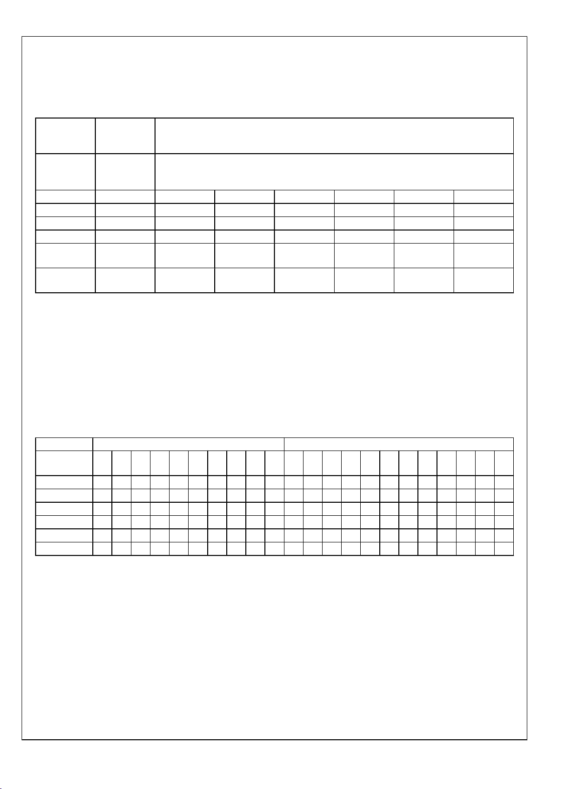
2.0 General Programming Information
The LMX2531 is programmed using 11 24-bit registers used to control the LMX2531 operation. A 24-bit shift register is used as a
temporary register to indirectly program the on-chip registers. The shift register consists of a data field and an address field. The
last 4 register bits, CTRL[3:0] form the address field, which is used to decode the internal register address. The remaining 20 bits
form the data field DATA[19:0]. While LE is low, serial data is clocked into the shift register upon the rising edge of clock (data is
programmed MSB first). When LE goes high, data is transferred from the data field into the selected register bank. Although there
are actually 14 registers in this part, only a portion of them should be programmed, since the state of the other hidden registers
(R13, R11, and R10) are set during the initialization sequence. Although it is possible to program these hidden registers, as well
as a lot of bits that are defined to either '1' or '0', the user should not experiment with these hidden registers and bits, since the
parts are not tested under these conditions and doing so will most likely degrade performance.
LMX2531
DATA[19:0] CONTROL[3:0]
MSB
D19 D18 D17 D16 D15 D14 D13 D12 D11 D10 D9 D8 D7 D6 D5 D4 D3 D2 D1 D0 C3 C2 C1 C0
2.01 Register Location Truth Table
C3 C2 C1 C0 Data Address
1 1 0 0 R12
1 0 0 1 R9
1 0 0 0 R8
0 1 1 1 R7
0 1 1 0 R6
0 1 0 1 R5
0 1 0 0 R4
0 0 1 1 R3
0 0 1 0 R2
0 0 0 1 R1
0 0 0 0 R0
2.02 Initialization Sequence
The initial loading sequence from a cold start is described below. The registers must be programmed in order shown. There must
be a minimum of 10 ms between the time when R5 is last loaded and R1 is loaded to ensure time for the LDOs to power up properly.
LSB
REG.
R5
INIT1
R5
INIT2
R5 1 0 0 0 0 0 0 0 0 0 0 0 0 1 1 1 1 1 1 1 0 1 0 1
R12 Program R12 as shown in the complete register map. 1 1 0 0
R9 Program R9 as shown in the complete register map. 1 0 0 1
R8
R7 See individual section for Register R7 programming information. 0 1 1 1
R6 See individual section for Register R6 programming information. 0 1 1 0
R4
R3 See individual section for Register R3 programming information. 0 0 1 1
R2 See individual section for Register R2 programming information. 0 0 1 0
R1 See individual section for Register R1 programming information. 0 0 0 1
R0 See individual section for Register R0 programming information. 0 0 0 0
23 22 21 20 19 18 17 16 15 14 13 12 11 10 9 8 7 6 5 4 3 2 1 0
DATA[19:0] C3 C2 C1 C0
1 0 0 0 0 1 0 0 0 0 0 0 0 0 0 0 0 0 0 0 0 1 0 1
1 0 0 0 0 0 0 0 0 0 0 0 0 0 0 0 0 0 0 0 0 1 0 1
See individual section for Register R8 programming information.
Programming of this register is necessary under specific circumstances.
See individual section for Register R4 programming information.
Register R4 only needs to be programmed if FastLock is used.
19 www.national.com
1 0 0 0
0 1 0 0
LMX2531
0 0 0 0
0 0 0 1
0 0 1 0
0 0 1 1
0 1 0 0
0 1 0 1
0 1 1 0
1 0 0 0
DATA[19:0] C3 C2 C1 C0
NUM
[11:0]
NUM
N
R
[21:12]
[10:8]
DEN
[5:0]
DEN
FoLD
[11:0]
[21:12]
TOC
[3:0]
[13:0]
EN_PLL
EN_VCO
EN_OSC
C3_4_ADJ
EN_VCOLD
EN_PLLLDO1
R3_ADJ_
EN_PLLLDO2
EN_DIGLDO
R3_ADJ
R4_ADJ_
R4_ADJ
FL
FL
[2:0]
[1:0]
[1:0]
[1:0]
[1:0]
XTL
0 0 0 0 0 1 1 1
[1:0]
XTLDIV
EN_LPFLTR
[11:0]
XTLMAN
MA
0 0 0 0 0 0 0 0 0 0
LOCK
MODE
N2
0 0 0 0 0 0 0
ICP
[3:0]
N
[7:0]
1
23 22 21 20 19 18 17 16 15 14 13 12 11 10 9 8 7 6 5 4 3 2 1 0
R0
RE
GIS
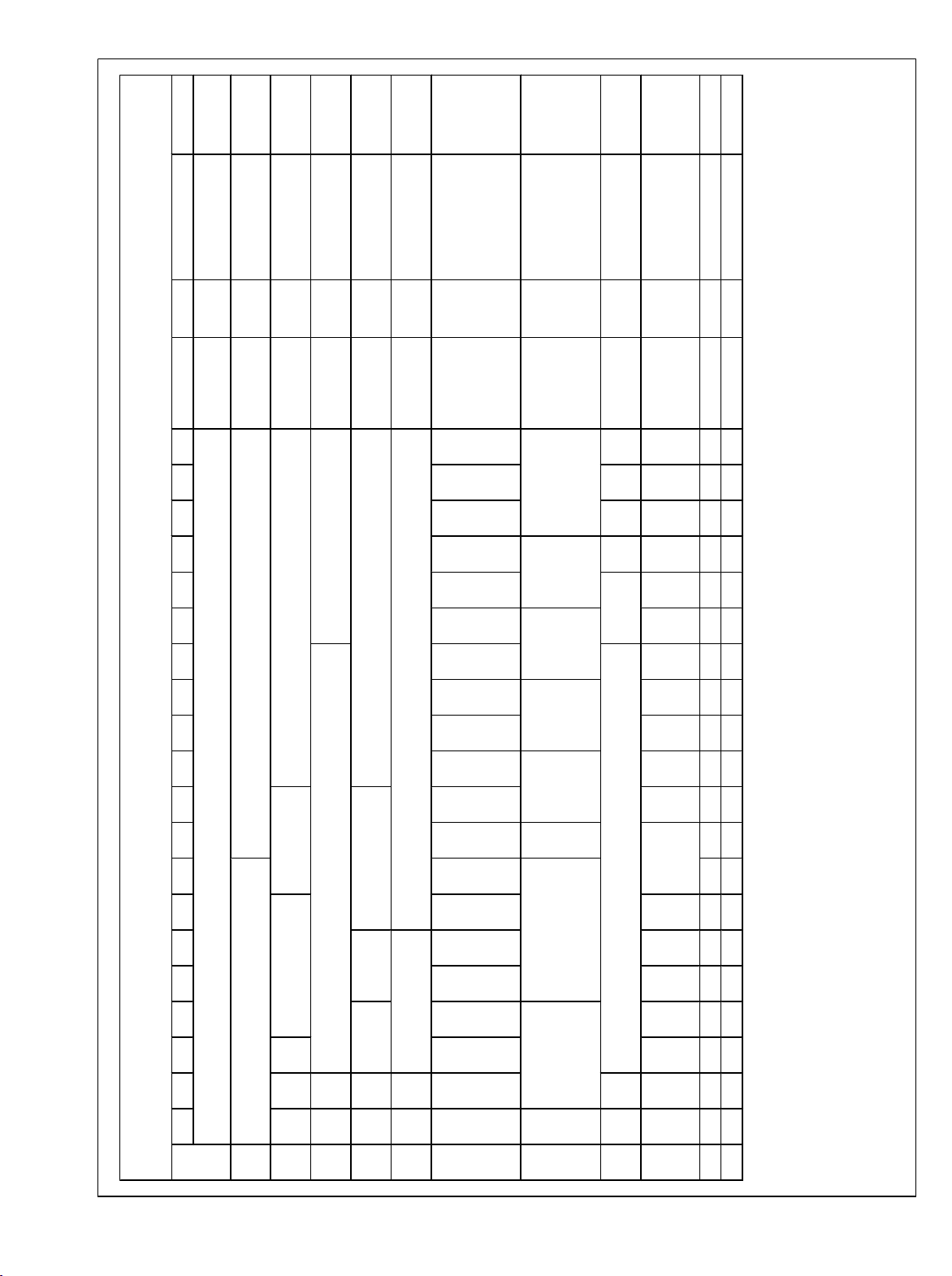
2.03 Complete Register Content Map
This table shows all the programmable bits for the LMX2531. No programming order or initialization sequence is implied by this table, only the location of the programming information.
www.national.com 20
TER
R1 0 0
R2 0 1
[1:0]
ORDER
[1:0]
DITHER
M
FD
2
DIV
R3
[3:0]
ICPFL
R4 0 0
R5 1 0 0 0 0
REG_RST
VCO_ACI_SEL
XTLSEL
R6 0
[3:0]
[2:0]
R7 0 0
R8 0 0 0 0 0 0 1
R9 0 0 0 0 0 0 0 0 0 0 0 0 1 0 1 1 1 0 1 0 1 0 0 1
R12 0 0 0 0 0 0 0 1 0 0 0 0 0 1 0 0 1 0 0 0 1 1 0 0
2.1 REGISTER R0
The action of programming the R0 register activates a frequency calibration routine for the VCO. This calibration is necessary to
get the VCO to center the tuning voltage for optimal performance. If the temperature drifts considerably, then the PLL should stay
in lock, provided that the temperature drift specification is not violated.
2.1.1 NUM[10:0] and NUM[21:12] -- Fractional Numerator
The NUM word is split between the R0 register and R1 register. The Numerator bits determine the fractional numerator for the
delta sigma PLL. This value can go from 0 to 4095 when the FDM bit ( R3[22] ) is 0 (the other bits in this register are ignored), or
0 to 4194303 when the FDM bit is 1.
NUM[21:12] NUM[11:0]
Fractional
Numerator
0 0 0 0 0 0 0 0 0 0 0 0 0 0 0 0 0 0 0 0 0 0 0
...
409503 1 1 1 1 1 1 1 1 1 1 1 1 1 1 1 1 1 1 1 1 1 1
4096 0 0 0 0 0 0 0 0 0 0 1 0 0 0 0 0 0 0 0 0 0 0
...
4194303 1 1 1 1 1 1 1 1 1 1 1 1 1 1 1 1 1 1 1 1 1 1
Note that there are restrictions on the fractional numerator value depending on the R divider value if it is 16 or 32.
2.1.2 N[7:0] and N[10:8]
The N counter is 11 bits. 8 of these bits are located in the R0 register, and the remaining 3 (MSB bits) are located in the R1 register.
The LMX2531 consists of an A, B, and C counter, which work in conjunction with the 16/17/20/21 prescaler in order to form the
final N counter value.
LMX2531
N[10:8] N[7:0]
N Value C B A
<55 Values less than 55 are prohibited.
55 0 0 0 0 0 1 1 0 1 1 1
...
2039 1 1 1 1 1 1 1 0 1 1 1
21 www.national.com
2.2 REGISTER R1
2.2.1 NUM[21:12]
LMX2531
These are the MSB bits in for the fractional numerator that already have been described.
2.2.2 N[10:8] -- 3 MSB Bits for the N Counter
These are the 2 MSB bits for the N counter, which were discussed in the R0 register section.
2.2.3 ICP[3:0] -- Charge Pump Current
This bit programs the charge pump current when the charge pump gain. The current is programmable between 100 uA and 1.6
mA in 100 uA steps. In general, higher charge pump currents yield better phase noise for the PLL, but also can cause higher spurs.
ICP Charge Pump State
0 1X 90
1 2X 180
2 3X 270
3 4X 360
4 5X 450
5 6X 540
6 7X 630
7 8X 720
8 9X 810
9 10X 900
10 11X 990
11 12X 1080
12 13X 1170
13 14X 1260
14 15X 1350
15 16X 1440
Typical Charge Pump Current at 3 Volts
(µA)
www.national.com 22
2.3 REGISTER R2
2.3.1 R[5:0] -- R Counter Value
These bits determine the phase detector frequency. The OSCin frequency is divided by this R counter value. Note that only the
values of 1, 2, 4, 8, 16, and 32 are allowed.
Fractional
R Value
0,3,5-7,
9-15,17-31,
33-63
1 none 0 0 0 0 0 1
2 none 0 0 0 0 1 0
4 none 0 0 0 1 0 0
8 none 0 0 1 0 0 0
16
32
Note that the R counter value can put some restrictions on the fractional denominator. In the case that it is 16, the fractional
denominator must be divisible by 2, which is equivalent to saying that the LSB of the fractional denominator word is zero. In the
case that the R counter is 32, the two LSB bits of the fractional denominator word must also be zero, which is equivalent to saying
that the fractional denominator must be divisible by 4. Because the fractional denominator can be very large, this should cause no
issues. For instance, if one wanted to achieve a fractional word of 1/65, and the R counter value was 16, the fractional word could
be changed t0 4/260 ,and the same resolution could be achieved.
Denominator
Restrictions
n/a These values are illegal.
Must be
divisible by 2
Must be
divisible by 4
0 1 0 0 0 0
1 0 0 0 0 0
R[5:0]
LMX2531
2.3.2 DEN[21:12] and DEN[11:0]-- Fractional Denominator
These bits determine the fractional denominator. Note that the MSB bits for this word are in register R3. If the FDM bit is set to 0,
DEN[21:12] are ignored. The fractional denominator should only be set to zero if the fractional circuitry is being disabled by setting
ORDER=1. A value of one never makes sense to use. All other values could reasonably be used in fractional mode.
DEN[21:12] DEN[11:0]
Fractional
Denominator
0 0 0 0 0 0 0 0 0 0 0 0 0 0 0 0 0 0 0 0 0 0 0
...
4095 1 1 1 1 1 1 1 1 1 1 1 1 1 1 1 1 1 1 1 1 1 1
4096 0 0 0 0 0 0 0 0 0 1 0 0 0 0 0 0 0 0 0 0 0 0
...
4194303 1 1 1 1 1 1 1 1 1 1 1 1 1 1 1 1 1 1 1 1 1 1
23 www.national.com
2.4 REGISTER R3
2.4.1 DEN[21:12] -- Extension for the Fractional Denominator
LMX2531
These are the MSB bits of the DEN word, which have already been discussed.
2.4.2 FoLD[3:0] -- Multiplexed Output for Ftest/LD Pin
The FoLD[3:0] word is used to program the output of the Ftest/LD Pin. This pin can be used for a general purpose I/O pin, a lock
detect pin, and for diagnostic purposes. When programmed to the digital lock detect state, the output of the Ftest/LD pin will be
high when the part is in lock, and low otherwise. Lock is determined by comparing the input phases to the phase detector. The
analog lock detect modes put out a high signal with very fast negative pulses, that correspond to when the charge pump comes
on. This output can be low pass filtered with an RC filter in order to determine the lock detect state. If the open drain state is used,
a additional pull-up resistor is required. For diagnostic purposes, the options that allow one to view the output of the R counter or
the N counter can be very useful. Be aware that the output voltage level of the Ftest/LD is not equal to the supply voltage of the
part, but rather is given by VOH and VOL in the electrical characteristics specification.
FoLD Output Type Function
0 High Impedance Disabled
1 Push-Pull Logical High State
2 Push-Pull Logical Low State
3 Push-Pull Digital Lock Detect
4 N/A Reserved
5 Push-Pull N Counter Output Divided by 2
6 Open-Drain Analog Lock Detect
7 Push-Pull Analog Lock Detect
8 N/A Reserved
9 N/A Reserved
10 N/A Reserved
11 N/A Reserved
12 N/A Reserved
13 N/A Reserved
14 Push-Pull R Counter Output
15 N/A Reserved
2.4.3 ORDER -- Order of Delta Sigma Modulator
This bit determines the order of the delta sigma modulator in the PLL. In general, higher order fractional modulators tend to reduce
the primary fractional spurs that occur at increments of the channel spacing, but can also create spurs that are at a fraction of the
channel spacing, if there is not sufficient filtering. The optimal choice of modulator order is very application specific, however, a
third order modulator is a good starting point if not sure what to try first.
ORDER Delta Sigma Modulator Order
0 Fourth
1
2 Second
3 Third
www.national.com 24
(Integer Mode - all fractions are ignored)
Reset Modulator
2.4.4 DITHER -- Dithering
Dithering is useful in reducing fractional spurs, especially those that occur a a fraction of the channel spacing. The only exception
is when the fractional numerator is zero. In this case, dithering usually is not a benefit. Dithering also can sometimes increase the
PLL phase noise by a fraction of a dB. In general, if dithering is disabled, phase noise may be slightly better inside the loop bandwidth
of the system, but spurs are likely to be worse too.
DITHER Dithering Mode
0 Weak Dithering
1 Reserved
2 Strong Dithering
3 Dithering Disabled
2.4.5 FDM -- Fractional Denominator Mode
When this bit is set to 1, the 10 MSB bits for the fractional numerator and denominator are considered. This allows the fractional
denominator to range from 1 to 4,194,303. If this bit is set to zero, only the 12 LSB bits of the fractional numerator and denominator
are considered, and this allows a fractional denominator from 1 to 4095. When this bit is disabled, the current consumption is about
0.5 mA lower.
2.4.6 -- DIV2
When this bit is enabled, the output of the VCO is divided by 2. Enabling this bit does have some impact on harmonic content and
output power.
DIV2 VCO Output Frequency
0 Not Divided by 2
1 Divided by 2
LMX2531
25 www.national.com

2.5 REGISTER R4
2.5.1 TOC[13:0] -- Time Out Counter for FastLock
LMX2531
When the value of this word is 3 or less, then FastLock is disabled, and this pin can only be used for general purpose I/O. When
this value is 4 or greater, the time out counter is engaged for the amount of phase detector cycles shown in the table below.
TOC Value FLout Pin State Timeout Count
0 High Impedance 0
1 Low Always Enabled
2 Low 0
3 High 0
4 Low 4 × 2 Phase Detector
. . .
16383 Low 16383 × 2 Phase Detector
When this count is active, the FLout Pin is grounded, the FastLock current is engaged, and the resistors R3 and R4 are also
potentially changed. The table below summarizes the bits that control various values in and out of FastLock differences.
FastLock State FLout Charge Pump Current R3 R4
Steady State High Impedance ICP R3_ADJ R4_ADJ
Fastlock Grounded ICPFL R3_ADJ_FL R4_ADJ_FL
2.5.2 ICPFL[3:0] -- Charge Pump Current for Fastlock
When FastLock is enabled, this is the charge pump current that is used for faster lock time.
ICPFL Fastlock Charge Pump State
0 1X 90
1 2X 180
2 3X 270
3 4X 360
4 5X 450
5 6X 540
6 7X 630
7 8X 720
8 9X 810
9 10X 900
10 11X 990
11 12X 1080
12 13X 1170
13 14X 1260
14 15X 1350
15 16X 1440
Typical Fastlock Charge Pump Current
at 3 Volts (µA)
www.national.com 26

2.6 REGISTER R5
2.6.1 EN_PLL -- Enable Bit for PLL
When this bit is set to 1, the PLL is powered up, otherwise, it is powered down.
2.6.2 EN_VCO -- Enable Bit for the VCO
When this bit is set to 1, the VCO is powered up, otherwise, it is powered down.
2.6.3 EN_OSC -- Enable Bit for the Oscillator Inverter
When this bit is set to 1 (default), the reference oscillator is powered up, otherwise it is powered down.
2.6.4 EN_VCOLDO -- Enable Bit for the VCO LDO
When this bit is set to 1 (default), the VCO LDO is powered up, otherwise it is powered down.
2.6.5 EN_PLLLDO1 -- Enable Bit for the PLL LDO 1
When this bit is set to 1 (default), the PLL LDO 1 is powered up, otherwise it is powered down.
2.6.6 EN_PLLLDO2 -- Enable Bit for the PLL LDO 2
When this bit is set to 1 (default), the PLL LDO 2 is powered up, otherwise it is powered down.
2.6.7 EN_DIGLDO -- Enable Bit for the digital LDO
When this bit is set to 1 (default), the Digital LDO is powered up, otherwise it is powered down.
2.6.8 REG_RST -- RESETS ALL REGISTERS TO DEFAULT SETTINGS
This bit needs to be programmed three times to initialize the part. When this bit is set to one, all registers are set to default mode,
and the part is powered down. The second time the R5 register is programmed with REG_RST=0, the register reset is released
and the default states are still in the registers. However, since the default states for the blocks and LDOs is powered off, it is
therefore necessary to program R5 a third time so that all the LDOs and blocks can be programmed to a power up state. When
this bit is set to 1, all registers are set to the default modes, but part is powered down. For normal operation, this bit is set to 0.
Note that once this initialization is done, it is not necessary to initialize the part any more.
LMX2531
27 www.national.com

2.7 REGISTER R6
2.7.1 C3_C4_ADJ[2:0] -- VALUE FOR C3 AND C4 IN THE INTERNAL LOOP FILTER
LMX2531
C3_C4_ADJ C3 (pF) C4 (pF)
0 50 50
1 50 100
2 50 150
3 100 50
4 150 50
5 100 100
6 50 150
7 50 150
2.7.2 R3_ADJ_FL[1:0] -- Value for Internal Loop Filter Resistor R3 During Fastlock
R3_ADJ_FL Value
0 10
1 20
2 30
3 40
2.7.3 R3_ADJ[1:0] -- Value for Internal Loop Filter Resistor R3
R3_ADJ
0 10
1 20
2 30
3 40
2.7.4 R4_ADJ_FL[1:0] -- Value for Internal Loop Filter Resistor R4 During Fastlock
R4_ADJ_FL
0 10
1 20
2 30
3 40
2.7.5 R4_ADJ[1:0] -- Value for Internal Loop Filter Resistor R4
R3 Resistor During Fastlock (kΩ)
R3 Value (kΩ)
R4 Value during Fast Lock (kΩ)
R4_ADJ
0 10
1 20
2 30
3 40
2.7.6 EN_LPFLTR-- Enable for Partially Integrated Internal Loop Filter
The Enable Loop Filter bit is used to enable or disable the 3rd and 4th pole on-chip loop filters.
EN_LPFLTR 3rd and 4th Poles of Loop Filter
0
1 enabled
www.national.com 28
(R3 = R4 = 0 Ω and C3 + C4 = 200pF)
R4 Value ( kΩ )
disabled

2.7.7 VCO_ACI_SEL
This bit is used to optimize the VCO phase noise. The recommended values are what are used for all testing purposes, and this
bit should be set as the table below instructs.
Part VCO_ACI_SEL
All Other Options 8
LMX2531LQ2265E
LMX2531LQ2570E
6
2.7.8 XTLSEL[2:0] -- Crystal Select
XTLSEL Crystal Frequency
0 <25 MHz
1 25 - 50 MHz
2 50 - 70 MHz
3 >70 MHz
4 Manual Mode
5 Reserved
6 Reserved
7 Reserved
The value of this word needs to be changed based on the frequency presented to the OSCin pin in accordance to the table above.
Manual mode must be used for the LMX2531LQ2080E and the LMX2531LQ2570 only. The other options should use modes 0 to
3.
LMX2531
2.8 REGISTER R7
2.8.1 XTLDIV[1:0] -- Division Ratio for the Crystal Frequency
The frequency provided to the VCO frequency calibration circuitry is based on the OSCin frequency divided down by a factor,
determined by the XTLDIV word. Note that this division ratio is independent of the R counter value or the phase detector frequency.
The necessary division ratio depends on the OSCin frequency and is shown in the table below:
XTLDIV Crystal Division Ratio Crystal Range
0 Reserved Reserved
1 Divide by 2 < 20 MHz
2 Divide by 4 20-40 MHz
3 Divide by 8 > 40 MHz
2.8.2 XTLMAN[11:0] -- Manual Crystal Mode
This word adjusts the calibration timing for lock time. With the exception of the parts listed in the table below, this bit should be set
to zero for normal operation. For f
16 × f
OSCin
/ Kbit.
Part Kbit
LMX2531LQ208
0E
LMX2531LQ257
0E
4.5 36 71 109 218 273
6.0 27 53 82 164 205
frequencies (expressed in MHz) not shown in the table, this bit value can be calculated as
OSCin
f
OSCin
10 MHz 20 MHz 30.72 MHz 61.44 MHz 76.8 MHz
29 www.national.com

2.9 REGISTER R8
2.9.1 XTLMAN2 -- MANUAL CRYSTAL MODE SECOND ADJUSTMENT
LMX2531
This bit also adjusts the calibration timing for lock time. In the case that manual mode for XTLSEL is selected and the OSCin
frequency is greater than 40 MHz, this bit should be enabled, otherwise it should be 0.
2.9.2 LOCKMODE -- FREQUENCY CALIBRATION MODE
This bit is controls the method for which the frequency calibration is done. It should set in a particular way based on which option
is used in accordance to the table below.
LOCKMODE LOCKMODE
0 Reserved
1 LMX2531LQ1146E/1226E/1312E/1415E/1515E
2 All Other Options
3 Reserved
2.10 REGISTER R9
All the bits in this register should be programmed as shown in the programming table.
2.11 REGISTER R12
Even though this register does not have user selectable bits, it still needs to be programmed. This register should be loaded as
shown the Complete Register Content Map ( section 2.03 ) .
www.national.com 30

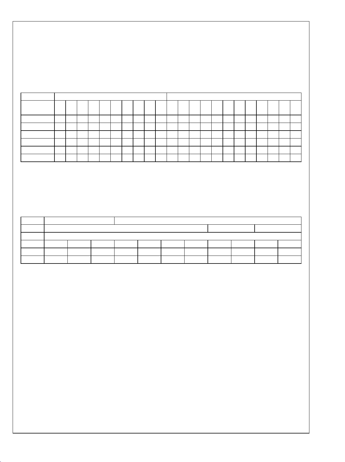
Physical Dimensions inches (millimeters) unless otherwise noted
LMX2531
Leadless Leadframe Package (NS Package Number LQA036D), D Version (Bottom View)
(LMX2531LQ1146E/1226E/1312E/1415E/1515E)
Order Number LMX2531LQX for 2500 Unit Reel
Order Number LMX2531LQ for 250 Unit Reel
Leadless Leadframe Package (NS Package Number LQA036A), A Version (Bottom View)
Order Number LMX2531LQX for 2500 Unit Reel
Order Number LMX2531LQ for 250 Unit Reel
(All Other Options)
31 www.national.com
Part Marking Package
LMX2531LQ1146E 311146E LQA036D
LMX2531
LMX2531LQ1226E 311226E LQA036D
LMX2531LQ1312E 311312E LQA036D
LMX2531LQ1415E 311415E LQA036D
LMX2531LQ1515E 311515E LQA036D
LMX2531LQ1570E 311570EB LQA036A
LMX2531LQ1650E 311650EA LQA036A
Part Marking Package
LMX2531LQ1700E 311778EB LQA036A
LMX2531LQ1742 311742EA LQA036A
LMX2531LQ1778E 311778EA LQA036A
LMX2531LQ1910E 311910EB LQA036A
LMX2531LQ2080E 312080EB LQA036A
LMX2531LQ2265E 312265ED LQA036A
LMX2531LQ2570E 312570EC LQA036A
www.national.com 32

Notes
LMX2531
33 www.national.com
Notes
For more National Semiconductor product information and proven design tools, visit the following Web sites at:
Products Design Support
Amplifiers www.national.com/amplifiers WEBENCH www.national.com/webench
Audio www.national.com/audio Analog University www.national.com/AU
Clock Conditioners www.national.com/timing App Notes www.national.com/appnotes
Data Converters www.national.com/adc Distributors www.national.com/contacts
Displays www.national.com/displays Green Compliance www.national.com/quality/green
Ethernet www.national.com/ethernet Packaging www.national.com/packaging
Interface www.national.com/interface Quality and Reliability www.national.com/quality
LVDS www.national.com/lvds Reference Designs www.national.com/refdesigns
Power Management www.national.com/power Feedback www.national.com/feedback
Switching Regulators www.national.com/switchers
LDOs www.national.com/ldo
LED Lighting www.national.com/led
PowerWise www.national.com/powerwise
Serial Digital Interface (SDI) www.national.com/sdi
Temperature Sensors www.national.com/tempsensors
Wireless (PLL/VCO) www.national.com/wireless
THE CONTENTS OF THIS DOCUMENT ARE PROVIDED IN CONNECTION WITH NATIONAL SEMICONDUCTOR CORPORATION
(“NATIONAL”) PRODUCTS. NATIONAL MAKES NO REPRESENTATIONS OR WARRANTIES WITH RESPECT TO THE ACCURACY
OR COMPLETENESS OF THE CONTENTS OF THIS PUBLICATION AND RESERVES THE RIGHT TO MAKE CHANGES TO
SPECIFICATIONS AND PRODUCT DESCRIPTIONS AT ANY TIME WITHOUT NOTICE. NO LICENSE, WHETHER EXPRESS,
IMPLIED, ARISING BY ESTOPPEL OR OTHERWISE, TO ANY INTELLECTUAL PROPERTY RIGHTS IS GRANTED BY THIS
DOCUMENT.
TESTING AND OTHER QUALITY CONTROLS ARE USED TO THE EXTENT NATIONAL DEEMS NECESSARY TO SUPPORT
NATIONAL’S PRODUCT WARRANTY. EXCEPT WHERE MANDATED BY GOVERNMENT REQUIREMENTS, TESTING OF ALL
PARAMETERS OF EACH PRODUCT IS NOT NECESSARILY PERFORMED. NATIONAL ASSUMES NO LIABILITY FOR
APPLICATIONS ASSISTANCE OR BUYER PRODUCT DESIGN. BUYERS ARE RESPONSIBLE FOR THEIR PRODUCTS AND
APPLICATIONS USING NATIONAL COMPONENTS. PRIOR TO USING OR DISTRIBUTING ANY PRODUCTS THAT INCLUDE
NATIONAL COMPONENTS, BUYERS SHOULD PROVIDE ADEQUATE DESIGN, TESTING AND OPERATING SAFEGUARDS.
EXCEPT AS PROVIDED IN NATIONAL’S TERMS AND CONDITIONS OF SALE FOR SUCH PRODUCTS, NATIONAL ASSUMES NO
LIABILITY WHATSOEVER, AND NATIONAL DISCLAIMS ANY EXPRESS OR IMPLIED WARRANTY RELATING TO THE SALE
AND/OR USE OF NATIONAL PRODUCTS INCLUDING LIABILITY OR WARRANTIES RELATING TO FITNESS FOR A PARTICULAR
PURPOSE, MERCHANTABILITY, OR INFRINGEMENT OF ANY PATENT, COPYRIGHT OR OTHER INTELLECTUAL PROPERTY
RIGHT.
LIFE SUPPORT POLICY
NATIONAL’S PRODUCTS ARE NOT AUTHORIZED FOR USE AS CRITICAL COMPONENTS IN LIFE SUPPORT DEVICES OR
SYSTEMS WITHOUT THE EXPRESS PRIOR WRITTEN APPROVAL OF THE CHIEF EXECUTIVE OFFICER AND GENERAL
COUNSEL OF NATIONAL SEMICONDUCTOR CORPORATION. As used herein:
Life support devices or systems are devices which (a) are intended for surgical implant into the body, or (b) support or sustain life and
whose failure to perform when properly used in accordance with instructions for use provided in the labeling can be reasonably expected
to result in a significant injury to the user. A critical component is any component in a life support device or system whose failure to perform
can be reasonably expected to cause the failure of the life support device or system or to affect its safety or effectiveness.
LMX2531 High Performance Frequency Synthesizer System with Integrated VCO
National Semiconductor and the National Semiconductor logo are registered trademarks of National Semiconductor Corporation. All other
brand or product names may be trademarks or registered trademarks of their respective holders.
Copyright© 2008 National Semiconductor Corporation
For the most current product information visit us at www.national.com
www.national.com
National Semiconductor
Americas Technical
Support Center
Email:
new.feedback@nsc.com
Tel: 1-800-272-9959
National Semiconductor Europe
Technical Support Center
Email: europe.support@nsc.com
German Tel: +49 (0) 180 5010 771
English Tel: +44 (0) 870 850 4288
National Semiconductor Asia
Pacific Technical Support Center
Email: ap.support@nsc.com
National Semiconductor Japan
Technical Support Center
Email: jpn.feedback@nsc.com
 Loading...