

查询LMX2430供应商
LMX2430/LMX2433/LMX2434
May 2003
LMX2430/LMX2433/LMX2434 PLLatinum Dual High Frequency Synthesizer for RF Personal
Communications
PLLatinum
™
Dual High Frequency Synthesizer for RF
Personal Communications
LMX2430 3.0 GHz/0.8 GHz
LMX2433 3.6 GHz/1.7 GHz
LMX2434 5.0 GHz/2.5 GHz
General Description
The LMX243x devices are high performance frequency synthesizers with integrated dual modulus prescalers. The
LMX243x devices are designed for use as RF and IF local
oscillators for dual conversion radio transceivers.
A 32/33 or a 16/17 prescale ratio can be selected for the 5.0
GHz LMX2434 RF synthesizer. An 8/9 or a 16/17 prescale
ratio can be selected for both the LMX2430 and LMX2433
RF synthesizers. The IF circuitry contains an 8/9 or a 16/17
prescaler. Using a proprietary digital phase locked loop technique, the LMX243x devices generate very stable, low noise
control signals for RF and IF voltage controlled oscillators.
Both the RF and IF synthesizers include a two-level programmable charge pump. Both the RF and IF synthesizers
have dedicated Fastlock circuitry with integrated timeout
counters. Furthermore, only a single word write is required to
power up and tune the synthesizers to a new frequency.
Serial data is transferred to the devices via a three-wire
interface (DATA, LE, CLK). A low voltage logic interface
allows direct connection to 1.8V devices. Supply voltages
from 2.25V to 2.75V are supported . The LMX243x family
features low current consumption:
LMX2430 (3.0 GHz/ 0.8 GHz) — 2.8 mA/ 1.4 mA, LMX2433
(3.6 GHz/ 1.7 GHz) —3.2 mA/ 2.0 mA, LMX2434 (5.0 GHz/
2.5 GHz) — 4.6 mA/ 2.4 mA at 2.50V.
The LMX243x devices are available in 20-Pin TSSOP and
20-Pin UTCSP surface mount plastic packages.
Features
n Low Current Consumption
n 2.25V to 2.75V Operation
n Selectable Synchronous or Asynchronous Powerdown
Mode
n Selectable Dual Modulus Prescaler:
LMX2430 RF: 8/9 or 16/17
LMX2433 RF: 8/9 or 16/17
LMX2434 RF: 16/17 or 32/33
LMX243x IF: 8/9 or 16/17
n Programmable Charge Pump Current Levels
RF and IF: 1 or 4 mA
n Fastlock
n Digital Filtered Lock Detect Output
n Analog Lock Detect Output (supports both Push-Pull
and Open Drain configurations)
n 1.8V MICROWIRE Logic Interface
n Available in 20-Pin TSSOP and 20-Pin UTCSP
™
Technology with Integrated Timeout Counters
Applications
n Mobile Handsets
(GSM, GPRS, W-CDMA, CDMA, PCS, AMPS, PDC,
DCS)
n Cordless Handsets
(DECT, DCT)
n Wireless Data
n Cable TV Tuners
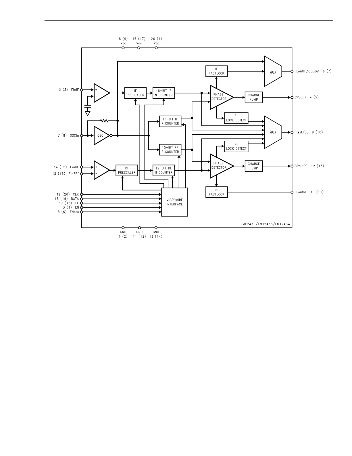
Thin Shrink Small Outline Package (MTC20) Ultra Thin Chip Scale Package (SLE20A)
20053580
20053581
PLLatinum™is a trademark of National Semiconductor Corporation.
© 2003 National Semiconductor Corporation DS200535 www.national.com
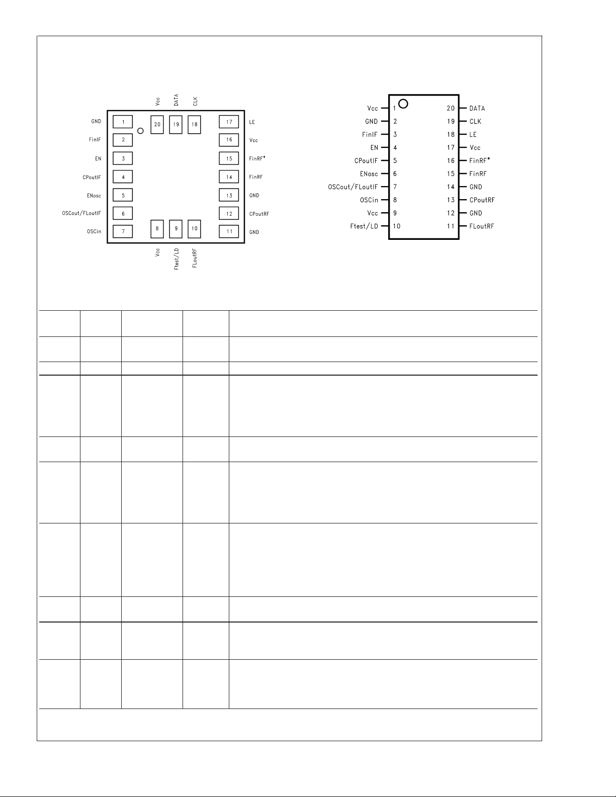
Functional Block Diagram
LMX2430/LMX2433/LMX2434
Note:
1 (2) refers to Pin
#
1 of the 20-Pin UTCSP and Pin#2 of the 20-Pin TSSOP
20053501
www.national.com 2
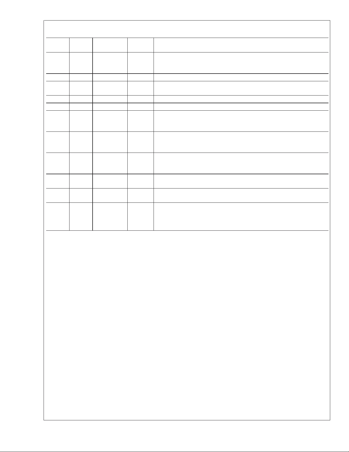
Connection Diagrams
LMX2430/LMX2433/LMX2434
Ultra Thin Chip Scale Package (SLE)
(Top View)
20053539
Thin Shrink Small Outline Package (TM)
(Top View)
20053583
Pin Descriptions
Pin No.
UTCSP
Pin No.
TSSOP
1 2 GND — Ground for the IF PLL analog and digital circuits, MICROWIRETM, Ftest/LD and
2 3 FinIF I IF PLL prescaler input. Small signal input from the VCO.
3 4 EN I Chip Enable input. High Impedance CMOS input. When this pin is set HIGH,
4 5 CPoutIF O IF PLL charge pump output. The output is connected to the external loop filter,
5 6 ENosc I Oscillator Enable input. High impedance CMOS input. When this pin is set
6 7 OSCout/
7 8 OSCin I Reference oscillator input. The input has an approximate Vcc/2 threshold and is
8 9 Vcc — Power supply bias for the RF PLL digital circuits and oscillator circuits. Vcc may
9 10 Ftest/LD O Programmable multiplexed output. Functions as a general purpose CMOS
Pin Name I/O Description
oscillator circuits.
the RF and IF PLLs are powered up. Powerdown is then controlled through the
MICROWIRE. When this pin is set LOW, the device is asynchronously powered
down and the charge pump output is forced to a high impedance state
(TRI-STATE).
which drives the input of the IF VCO.
HIGH, the oscillator buffer is always powered up, independent of the state of
the EN pin. When this pin is set LOW, the OSCout/ FLoutIF pin functions as an
IF Fastlock output, which connects a resistor in parallel to R2 of the external
loop filter.
O Oscillator output/ IF PLL Fastlock output. The output configuration is dependent
FLoutIF
on the state of the ENosc pin. When ENosc is set LOW, the pin functions as an
IF Fastlock output, which connects a resistor in parallel to R2 of the external
loop filter. This configuration also functions as a general purpose CMOS
TRI-STATE output. When ENosc is set HIGH, the pin functions as an oscillator
output so that an external crystal can be used.
driven by an external AC coupled source.
range from 2.25V to 2.75V. Bypass capacitors should be placed as close as
possible to this pin and be connected directly to the ground plane.
TRI-STATE output, N and R divider output, RF/ IF PLL push-pull analog lock
detect output, RF/ IF PLL open-drain analog lock detect output, or RF/ IF PLL
digital filtered lock detect output.
www.national.com3
Pin Descriptions (Continued)
Pin No.
UTCSP
10 11 FLoutRF O RF PLL Fastlock output. This pin connects a resistor in parallel to R2 of the
11 12 GND — Ground for the RF PLL digital circuits.
12 13 CPoutRF O RF PLL charge pump output. The output is connected to the external loop filter,
LMX2430/LMX2433/LMX2434
13 14 GND — Ground for the RF PLL analog circuits.
14 15 FinRF I RF PLL prescaler input. Small signal input from the VCO.
15 16 FinRF
16 17 Vcc — Power supply bias for the RF PLL analog circuits. Vcc may range from 2.25V to
17 18 LE I MICROWIRE Latch Enable input. High impedance CMOS input. When LE
18 19 CLK I MICROWIRE Clock input. High impedance CMOS input. DATA is clocked into
19 20 DATA I MICROWIRE Data input. High impedance CMOS input. Binary serial data. The
20 1 Vcc — Power supply bias for the IF PLL analog and digital circuits, MICROWIRE, and
Pin No.
TSSOP
Pin Name I/O Description
external loop filter. This pin can also function as a general purpose CMOS
TRI-STATE output.
which drives the input of the RF VCO.
*
I RF PLL prescaler complementary input. For single ended operation, this pin
should be AC grounded through a 100 pF capacitor. The LMX243x can be
driven differentially when the AC coupled capacitor is omitted.
2.75V. Bypass capacitors should be placed as close as possible to this pin and
be connected directly to the ground plane.
transitions HIGH, DATA stored in the shift register is loaded into one of 6
internal control registers.
the 24-bit shift register on the rising edge of CLK.
MSB of DATA is shifted in first. The two last bits are the control bits.
Ftest/LD circuits. Vcc may range from 2.25V to 2.75V. Bypass capacitors
should be placed as close as possible to this pin and be connected directly to
the ground plane
www.national.com 4

Ordering Information
Model Temperature Range Package Description Packing NS Package Number
LMX2430TM -40˚C to +85˚C Thin Shrink Small
LMX2430TMX -40˚C to +85˚C Thin Shrink Small
LMX2430SLEX -40˚C to +85˚C Ultra Thin Chip Scale
LMX2433TM -40˚C to +85˚C Thin Shrink Small
LMX2433TMX -40˚C to +85˚C Thin Shrink Small
LMX2433SLEX -40˚C to +85˚C Ultra Thin Chip Scale
LMX2434TM -40˚C to +85˚C Thin Shrink Small
LMX2434TMX -40˚C to +85˚C Thin Shrink Small
LMX2434SLEX -40˚C to +85˚C Ultra Thin Chip Scale
LMX2430/LMX2433/LMX2434
73 Units Per Rail MTC20
Outline Package
(TSSOP)
2500 Units Per Reel MTC20
Outline Package
(TSSOP)
Tape and Reel
2500 Units Per Reel SLE20A
Package (UTCSP)
Tape and Reel
73 Units Per Rail MTC20
Outline Package
(TSSOP)
2500 Units Per Reel MTC20
Outline Package
(TSSOP)
Tape and Reel
2500 Units Per Reel SLE20A
Package (UTCSP)
Tape and Reel
73 Units Per Rail MTC20
Outline Package
(TSSOP)
2500 Units Per Reel MTC20
Outline Package
(TSSOP)
Tape and Reel
2500 Units Per Reel SLE20A
Package (UTCSP)
Tape and Reel
www.national.com5
Absolute Maximum Ratings (Notes 1,
2, 3)
If Military/Aerospace specified devices are required,
please contact the National Semiconductor Sales Office/
Distributors for availability and specifications.
Power Supply Voltage
Vcc to GND −0.3V to +3.25V
Voltage on any pin to GND (V
V
must be<+3.25V −0.3V to Vcc+0.3V
I
LMX2430/LMX2433/LMX2434
Storage Temperature Range (T
Lead Temperature (solder 4 s) (T
)
I
) −65˚C to +150˚C
S
) +260˚C
L
Electrical Characteristics
Vcc = EN = 2.5V, −40˚C ≤ TA≤ +85˚C, unless otherwise specified
Symbol Parameter Conditions
I
PARAMETERS
CC
Icc
RF
Icc
IF
Icc
PD
RF SYNTHESIZER PARAMETERS
f
FinRF
N
RF
R
RF
f
COMPRF
p
FinRF
Power Supply
Current, RF
Synthesizer
Power Supply
Current, IF
Synthesizer
LMX2430 CLK, DATA and LE = 0V
OSCin = GND
LMX2433 3.2 4.4 mA
LMX2434 4.6 6.2 mA
RF_PD Bit = 0
IF_PD Bit = 1
RF_P Bit = 0
LMX2430 CLK, DATA and LE = 0V
OSCin = GND
LMX2433 2.0 2.8 mA
LMX2434 2.4 3.5 mA
RF_PD Bit = 1
IF_PD Bit = 0
IF_P Bit = 0
Powerdown Current EN, ENosc, CLK, DATA
and LE = 0V
RF Operating
Frequency
LMX2430 RF_P Bit = 0 250 2500 MHz
RF_P Bit = 1 250 3000 MHz
LMX2433 RF_P Bit = 0 500 3000 MHz
RF_P Bit = 1 500 3600 MHz
LMX2434 RF_P Bit = 0 or 1 1000 5000 MHz
N Divider Range P = 8/9
(Note 4)
P = 16/17
(Note 4)
P = 32/33
(Note 4)
RF R Divider Range 3 32767
RF Phase Detector Frequency 10 MHz
RF Input Sensitivity LMX2430/33
2.25V ≤ Vcc ≤ 2.75V
(Note 5)
LMX2434
2.35V ≤ Vcc ≤ 2.75V
(Note 5)
Recommended Operating
Conditions
Power Supply Voltage
Vcc to GND +2.25V to +2.75V
Operating Temperature (T
Note 1: Absolute Maximum Ratings indicate limits beyond which damage to
the device may occur. Recommended Operating Conditions indicate conditions for which the device is intended to be functional, but do not guarantee
specific performance limits. For guaranteed specifications and test conditions, refer to the Electrical Characteristics section. The guaranteed specifications apply only for the conditions listed.
Note 2: This device is a high performance RF integrated circuit with an ESD
<
rating
2 kV and is ESD sensitive. Handling and assembly of this device
should only be done at ESD protected work stations.
Note 3: GND=0V
(Note 1)
) −40˚C to +85˚C
A
Value
Min Typ Max
2.8 3.6 mA
1.4 2.0 mA
24 262151
48 524287
96 524287
−15 0 dBm
−12 0 dBm
Units
10 µA
www.national.com 6
Electrical Characteristics (Continued)
Vcc = EN = 2.5V, −40˚C ≤ TA≤ +85˚C, unless otherwise specified
Symbol Parameter Conditions
RF SYNTHESIZER PARAMETERS
I
CPoutRF
Source
I
CPoutRF
Sink
I
CPoutRF
TRI
I
CPoutRF
%MIS
I
CPoutRF
%V
CPoutRF
I
CPoutRF
%T
A
IF SYNTHESIZER PARAMETERS
f
FinIF
N
IF
R
IF
f
COMPIF
p
FinIF
I
CPoutIF
Source
I
CPoutIF
Sink
RF Charge Pump Output Source
Current
V
CPoutRF
= Vcc/2
RF_CPG Bit = 0
(Note 6)
CPoutRF
= Vcc/2
V
RF_CPG Bit = 1
(Note 6)
RF Charge Pump Output Sink Current V
CPoutRF
= Vcc/2
RF_CPG Bit = 0
(Note 6)
CPoutRF
= Vcc/2
V
RF_CPG Bit = 1
(Note 6)
RF Charge Pump Output TRI-STATE
Current
RF Charge Pump Output Sink Current
Vs Charge Pump Output Source
0.5V ≤ V
(Note 6)
V
CPoutRF
(Note 7)
CPoutRF
= Vcc/2
≤ Vcc - 0.5V
Current Mismatch
RF Charge Pump Output Current
Magnitude Variation Vs Charge Pump
0.5V ≤ V
(Note 7)
CPoutRF
≤ Vcc - 0.5V
Output Voltage
RF Charge Pump Output Current
Magnitude Variation Vs Temperature
IF Operating
Frequency
LMX2430 IF_P Bit = 0 or 1 100 800 MHz
LMX2433 IF_P Bit = 0 or 1 250 1700 MHz
V
CPoutRF
(Note 7)
= Vcc/2
LMX2434 IF_P Bit = 0 or 1 500 2500 MHz
IF N Divider Range P = 8/9
(Note 4)
P = 16/17
(Note 4)
IF R Divider Range 3 32767
IF Phase Detector Frequency 10 MHz
IF Input Sensitivity 2.25V ≤ Vcc ≤ 2.75V
(Note 5)
IF Charge Pump Output Source
Current
V
CPoutIF
= Vcc/2
IF_CPG Bit = 0
(Note 6)
CPoutIF
= Vcc/2
V
IF_CPG Bit = 1
(Note 6)
IF Charge Pump Output Sink Current V
CPoutIF
= Vcc/2
IF_CPG Bit = 0
(Note 6)
CPoutIF
= Vcc/2
V
IF_CPG Bit = 1
(Note 6)
Value
Min Typ Max
Units
-1.0 mA
-4.0 mA
1.0 mA
4.0 mA
-2.5 2.5 nA
310%
515%
2%
24 131079
48 262143
-15 0 dBm
-1.0 mA
-4.0 mA
1.0 mA
4.0 mA
LMX2430/LMX2433/LMX2434
www.national.com7
Electrical Characteristics (Continued)
Vcc = EN = 2.5V, −40˚C ≤ TA≤ +85˚C, unless otherwise specified
Symbol Parameter Conditions
IF SYNTHESIZER PARAMETERS
I
CPoutIF
TRI
I
CPoutIF
%MIS
LMX2430/LMX2433/LMX2434
I
CPoutIF
%V
CPoutIF
I
CPoutIF
%T
A
OSCILLATOR PARAMETERS
f
OSCin
v
OSCin
I
OSCin
DIGITAL INTERFACE (DATA, CLK, LE, EN, ENosc, Ftest/LD, FLoutRF, OSCout/ FLoutIF)
V
IH
V
IL
I
IH
I
IL
V
OH
V
OL
MICROWIRE INTERFACE
t
CS
t
CH
t
CWH
t
CWL
t
ES
t
EW
IF Charge Pump Output TRI-STATE
Current
IF Charge Pump Output Sink Current
Vs Charge Pump Output Source
0.5V ≤ V
(Note 6)
V
CPoutIF
(Note 7)
CPoutIF
= Vcc/2
≤ Vcc - 0.5V
Current Mismatch
IF Charge Pump Output Current
Magnitude Variation Vs Charge Pump
0.5V ≤ V
(Note 7)
CPoutIF
≤ Vcc - 0.5V
Output Voltage
IF Charge Pump Output Current
Magnitude Variation Vs Temperature
V
CPoutIF
(Note 7)
= Vcc/2
Oscillator Operating Frequency 1 256 MHz
Oscillator Sensitivity (Note 8) 0.5 Vcc V
Oscillator Input Current V
= Vcc 100 µA
OSCin
V
= 0V -100 µA
OSCin
High-Level Input Voltage 1.6 V
Low-Level Input Voltage 0.4 V
High-Level Input Current VIH= Vcc 1.0 µA
Low-Level Input Current VIL= 0V −1.0 µA
High-Level Output Voltage IOH= −500 µA VCC−
Low-Level Output Voltage IOL= 500 µA 0.4 V
DATA to CLK Set Up Time (Note 9) 50 ns
DATA to CLK Hold Time (Note 9) 10 ns
CLK Pulse Width HIGH (Note 9) 50 ns
CLK Pulse Width LOW (Note 9) 50 ns
CLK to LE Set Up Time (Note 9) 50 ns
LE Pulse Width (Note 9) 50 ns
Value
Min Typ Max
Units
-2.5 2.5 nA
310%
515%
2%
0.4
PP
V
www.national.com 8

Electrical Characteristics (Continued)
Vcc = EN = 2.5V, −40˚C ≤ TA≤ +85˚C, unless otherwise specified
Symbol Parameter Conditions
PHASE NOISE CHARACTERISTICS
L
(f) RF Synthesizer Normalized Phase
NRF
Noise Contribution
(Note 10)
(f) IF Synthesizer Normalized Phase
L
NIF
Noise Contribution
(Note 10)
(f) RF Synthesizer Single
L
RF
Side Band Phase
Noise Measured
LMX2430 f
LMX2433 f
LMX2434 f
TCXO Reference Source
RF_CPG Bit = 1
IF_PD Bit = 1
TCXO Reference Source
IF_CPG Bit = 1
RF_PD Bit = 1
= 2750 MHz
FinRF
f = 10 kHz offset
f
COMPRF
= 1 MHz
Loop Bandwidth = 100 kHz
= 2750
N
RF
=10MHz
f
OSCin
=1V
v
OSCin
PP
RF_CPG Bit = 1
IF_PD Bit = 1
= +25oC
T
A
(Note 11)
= 3200 MHz
FinRF
f = 10 kHz offset
f
COMPRF
= 1 MHz
Loop Bandwidth = 100 kHz
= 3200
N
RF
=10MHz
f
OSCin
=1V
v
OSCin
PP
RF_CPG Bit = 1
IF_PD Bit = 1
= +25oC
T
A
(Note 11)
= 4700 MHz
FinRF
f = 10 kHz offset
f
COMPRF
= 1 MHz
Loop Bandwidth = 100 kHz
= 4700
N
RF
=10MHz
f
OSCin
=1V
v
OSCin
PP
RF_CPG Bit = 1
IF_PD Bit = 1
= +25oC
T
A
(Note 11)
Value
Min Typ Max
-219.0 dBc/
-214.0 dBc/
-90.30 dBc/
-88.90 dBc/
-85.60 dBc/
LMX2430/LMX2433/LMX2434
Units
Hz
Hz
Hz
Hz
Hz
Note 4: Some of the values in this range are illegal divide ratios (B<A). To obtain continuous legal division, the Minimum Divide Ratio must be calculated. Use N
*
≥ P
(P−1), where P is the value of the prescaler selected.
Note 5: Refer to the LMX243x FinRF Sensitivity Test Setup section
Note 6: Refer to the LMX243x Charge Pump Test Setup section
Note 7: Refer to the Charge Pump Current Specification Definitions for details on how these measurements are made.
Note 8: Refer to the LMX243x OSCin Sensitivity Test Setup section
Note 9: Refer to the LMX243x Serial Data Input Timing section
Note 10: Normalized Phase Noise Contribution is defined as : L
measured at an offset frequency, f, ina1Hzbandwidth. The offset frequency, f, must be chosen sufficiently smaller than the PLL’s loop bandwidth, yet large enough
to avoid substantial phase noise contribution from the reference source. N is the value selected for the feedback divider and f
detector comparison frequency.
Note 11: The synthesizer phase noise is measured with the LMX2430TM/LMX2430SLE Evaluation boards and the HP8566B Spectrum Analyzer.
(f) = L(f) − 20 log (N) − 10 log (f
N
), where L(f) is defined as the single side band phase noise
COMP
is the RF/IF phase/ frequency
COMP
www.national.com9
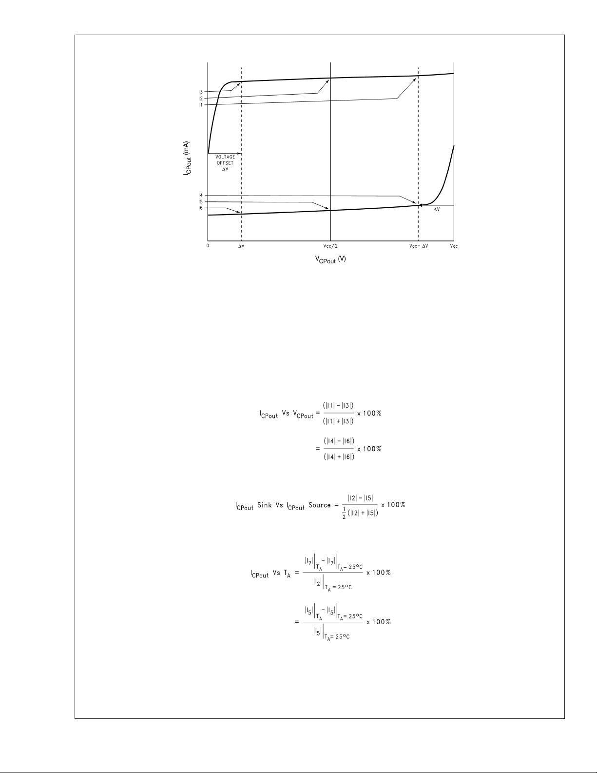
Charge Pump Current Specification Definitions
LMX2430/LMX2433/LMX2434
I1 = Charge Pump Sink Current at V
I2 = Charge Pump Sink Current at V
I3 = Charge Pump Sink Current at V
I4 = Charge Pump Source Current at V
I5 = Charge Pump Source Current at V
I6 = Charge Pump Source Current at V
CPout
CPout
CPout
CPout
CPout
CPout
= Vcc − ∆V
= Vcc//2
= ∆V
= Vcc − ∆V
= Vcc/2
= ∆V
20053537
∆V = Voltage offset from the positive and negative rails. Dependent on the VCO tuning range relative to Vcc and GND. Typical values are between 0.5V and
1.0V.
V
CPout
I
refers to either I
CPout
refers to either V
CPoutRF
CPoutRF
or I
or V
CPoutIF
CPoutIF
Charge Pump Output Current Magnitude Variation Vs Charge Pump Output Voltage
20053563
Charge Pump Output Sink Current Vs Charge Pump Output Source Current Mismatch
20053564
Charge Pump Output Current Magnitude Variation Vs Temperature
www.national.com 10
20053565
Typical Performance Characteristics
Sensitivity
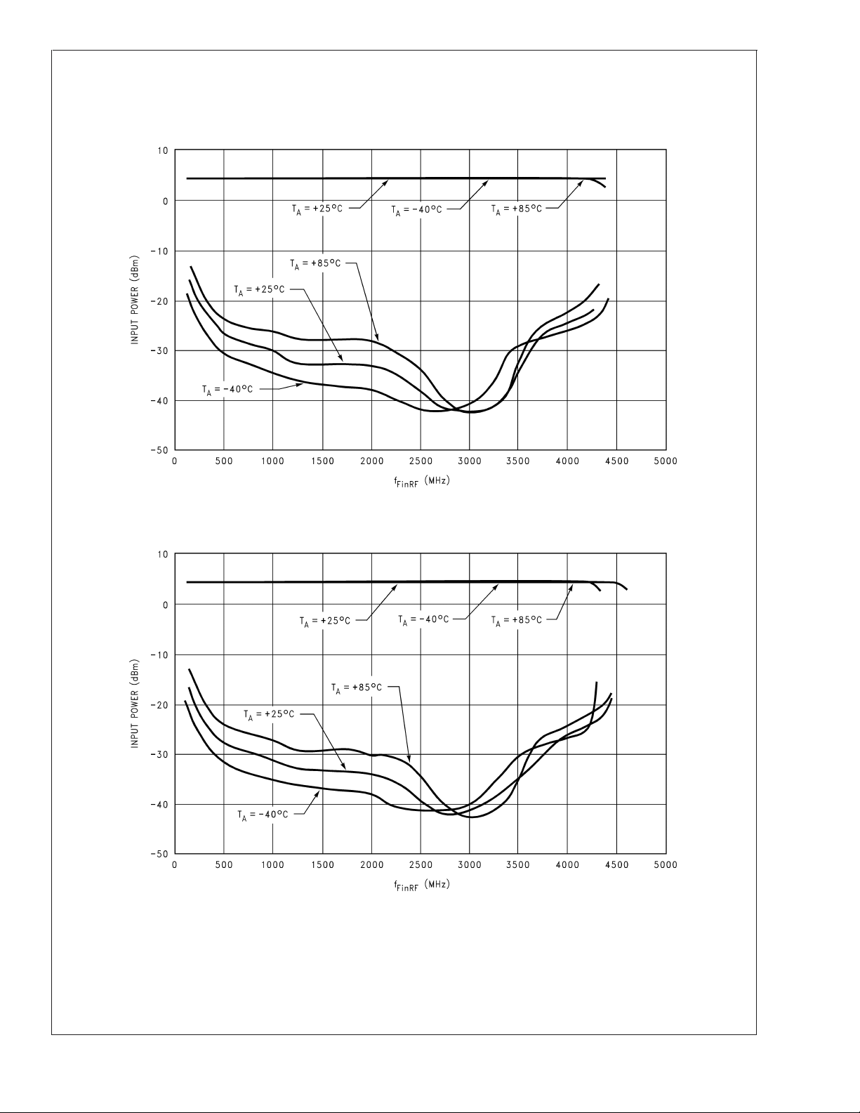
LMX2430 FinRF Input Power Vs Frequency
Vcc = EN = 2.25V
LMX2430/LMX2433/LMX2434
LMX2430 FinRF Input Power Vs Frequency
Vcc = EN = 2.75V
20053592
20053593
www.national.com11
Typical Performance Characteristics
Sensitivity
LMX2430/LMX2433/LMX2434
(Continued)
LMX2433 FinRF Input Power Vs Frequency
Vcc = EN = 2.25V
LMX2433 FinRF Input Power Vs Frequency
Vcc = EN = 2.75V
20053594
20053595
www.national.com 12
Typical Performance Characteristics
Sensitivity
(Continued)
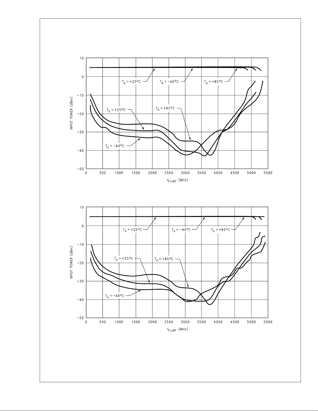
LMX2434 FinRF Input Power Vs Frequency
Vcc = EN = 2.35V
LMX2430/LMX2433/LMX2434
LMX2434 FinRF Input Power Vs Frequency
Vcc = EN = 2.75V
20053596
20053597
www.national.com13
Typical Performance Characteristics
Sensitivity
LMX2430/LMX2433/LMX2434
(Continued)
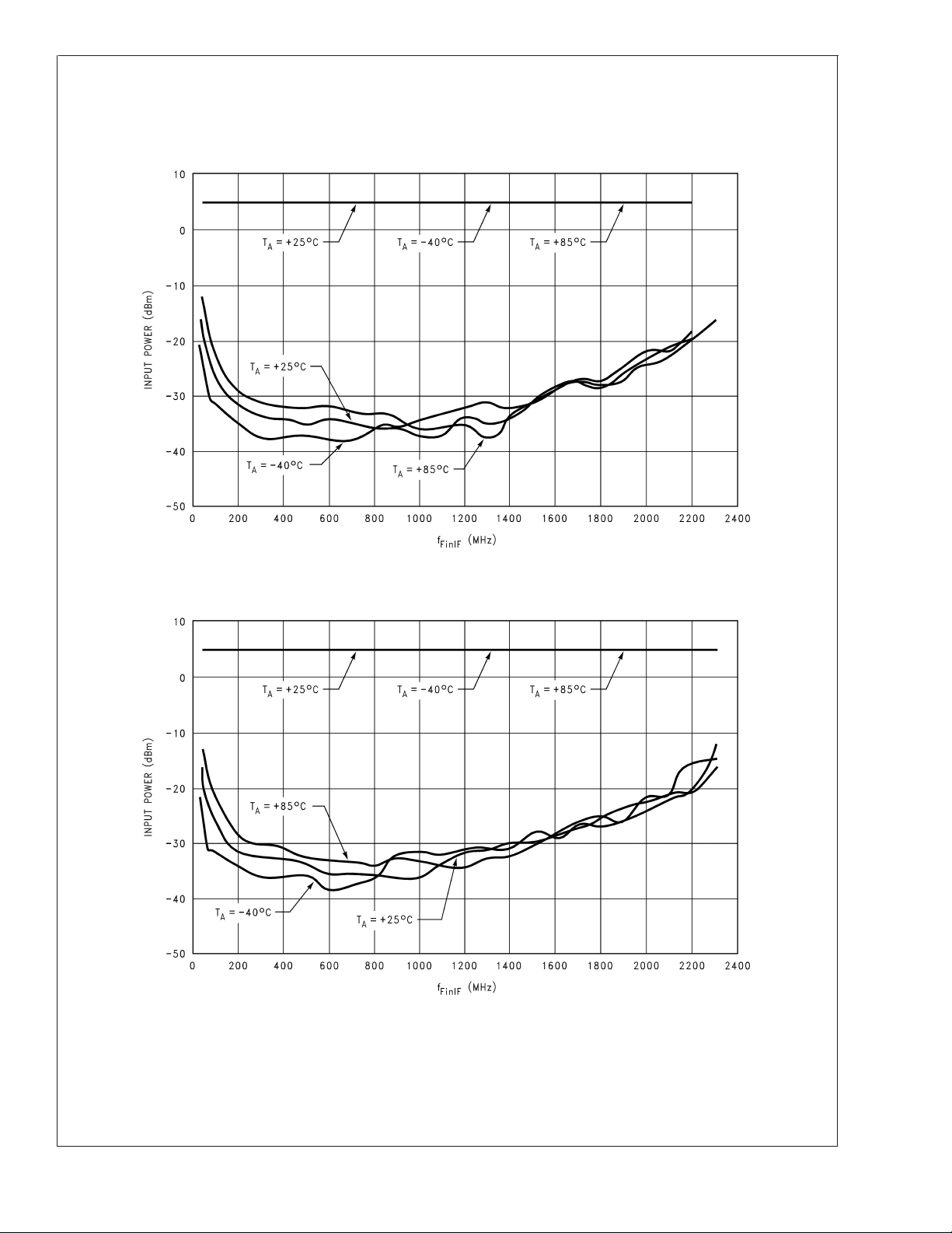
LMX2430 FinIF Input Power Vs Frequency
Vcc = EN = 2.25V
LMX2430 FinIF Input Power Vs Frequency
Vcc = EN = 2.75V
20053598
20053599
www.national.com 14
Typical Performance Characteristics
Sensitivity
(Continued)
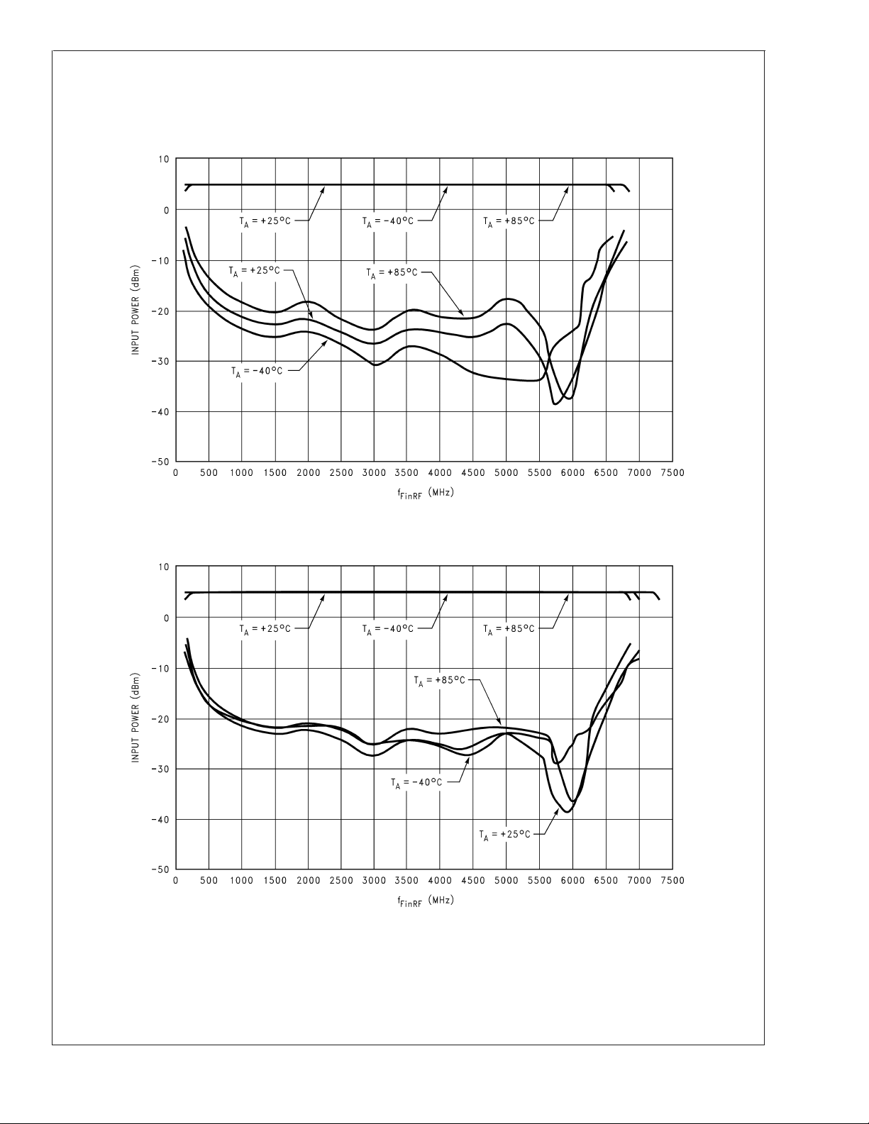
LMX2433 FinIF Input Power Vs Frequency
Vcc = EN = 2.25V
LMX2430/LMX2433/LMX2434
LMX2433 FinIF Input Power Vs Frequency
Vcc = EN = 2.75V
200535A0
200535A1
www.national.com15

Typical Performance Characteristics
Sensitivity
LMX2430/LMX2433/LMX2434
(Continued)
LMX2434 FinIF Input Power Vs Frequency
Vcc = EN = 2.25V
LMX2434 FinIF Input Power Vs Frequency
Vcc = EN = 2.75V
200535A2
200535A3
www.national.com 16

Typical Performance Characteristics
Sensitivity
(Continued)
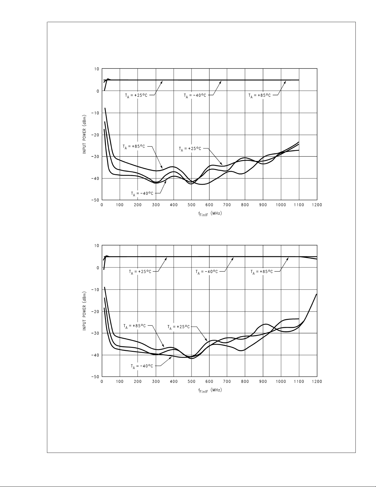
LMX243x OSCin Input Voltage Vs Frequency
Vcc = EN = 2.25V
LMX2430/LMX2433/LMX2434
LMX243x OSCin Input Voltage Vs Frequency
Vcc = EN = 2.75V
200535A4
200535A5
www.national.com17

Typical Performance Characteristics
Charge Pump
LMX243x RF Charge Pump Sweeps
LMX2430/LMX2433/LMX2434
Vcc = EN = 2.50V
−40˚C ≤ T
≤ +85˚C
A
LMX243x IF Charge Pump Sweeps
Vcc = EN = 2.50V
−40˚C ≤ T
≤ +85˚C
A
200535A6
www.national.com 18
200535A7

Typical Performance Characteristics
Input Impedance
LMX2430/LMX2433/LMX2434
LMX243x UTCSP FinRF Input Impedance
Vcc = EN = 2.50V, T
= +25˚C
A
LMX243x TSSOP FinRF Input Impedance
Vcc = EN = 2.50V, TA= +25˚C
LMX243x UTCSP FinIF Input Impedance
Vcc = EN = 2.50V, T
= +25˚C
A
200535A8 200535A9
LMX243x TSSOP FinIF Input Impedance
Vcc = EN = 2.50V, TA= +25˚C
200535B0 200535B1
www.national.com19
Typical Performance Characteristics
Input Impedance
LMX2430/LMX2433/LMX2434
(Continued)
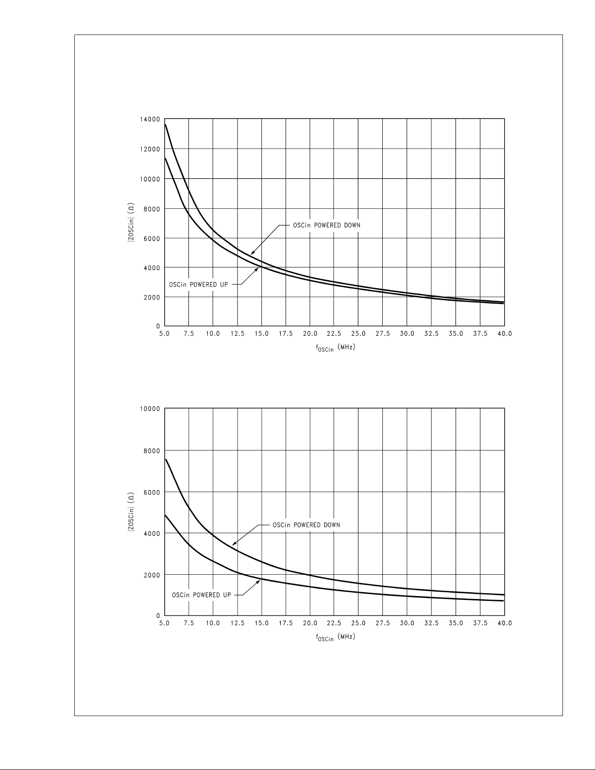
LMX243x UTCSP OSCin Input Impedance Vs Frequency
Vcc = EN = 2.50V
= +25˚C
T
A
LMX233xU TSSOP OSCin Input Impedance Vs Frequency
Vcc = EN = 2.50V
= +25˚C
T
A
200535B2
www.national.com 20
200535B3

LMX243x UTCSP FinRF Input Impedance Table
Vcc = EN = 2.50V, TA= +25˚C
f
FinRF
(MHz)
100 0.86 -8.63 334.27 -339.55 476.48
200 0.86 -10.72 265.44 -313.48 410.77
300 0.85 -13.48 202.09 -281.42 346.46
400 0.84 -17.01 150.76 -245.31 287.93
500 0.83 -21.05 112.18 -212.85 240.60
600 0.82 -25.32 85.96 -185.41 204.37
700 0.82 -29.78 67.32 -162.49 175.88
800 0.81 -34.35 54.27 -143.15 153.09
900 0.80 -39.02 44.76 -127.07 134.72
1000 0.80 -43.83 37.32 -113.62 119.59
1100 0.79 -48.76 31.65 -102.07 106.86
1200 0.79 -53.90 27.30 -91.89 95.86
1300 0.78 -59.07 23.84 -82.83 86.19
1400 0.78 -64.41 21.34 -74.84 77.82
1500 0.77 -70.04 19.20 -67.56 70.24
1600 0.76 -75.84 17.46 -60.88 63.33
1700 0.75 -82.06 16.27 -54.72 57.09
1800 0.73 -88.56 15.36 -48.89 51.25
1900 0.72 -95.19 14.90 -43.34 45.83
2000 0.70 -101.45 14.32 -38.66 41.23
2100 0.68 -107.85 14.10 -34.26 37.05
2200 0.67 -114.12 13.81 -30.35 33.34
2300 0.66 -120.12 13.27 -27.09 30.17
2400 0.66 -126.01 12.50 -24.00 27.06
2500 0.67 -131.82 11.68 -21.22 24.22
2600 0.69 -137.96 10.55 -18.24 21.07
2700 0.71 -144.21 9.53 -15.58 18.26
2800 0.72 -150.25 8.55 -12.92 15.49
2900 0.74 -156.23 7.75 -10.25 12.85
3000 0.75 -161.92 7.22 -7.77 10.61
3100 0.76 -167.18 6.87 -5.48 8.79
3200 0.77 -172.05 6.63 -3.42 7.46
3300 0.77 -177.55 6.40 -1.49 6.57
3400 0.78 179.16 6.18 0.35 6.19
3500 0.79 174.92 5.99 2.18 6.37
3600 0.79 170.77 5.85 3.99 7.08
3700 0.80 166.54 5.74 5.80 8.16
3800 0.80 162.52 5.73 7.56 9.49
3900 0.80 158.74 5.73 9.22 10.86
4000 0.80 155.06 5.68 10.84 12.24
4100 0.80 151.49 5.69 12.38 13.62
4200 0.80 148.28 5.70 13.78 14.91
4300 0.80 146.02 5.73 14.88 15.95
4400 0.80 144.12 5.60 15.84 16.80
4500 0.82 142.31 5.41 16.66 17.52
4600 0.83 140.78 5.29 17.42 18.21
4700 0.83 139.65 5.14 17.95 18.67
4800 0.84 138.75 4.99 18.38 19.05
|Γ| Angle (Γ)
(o)
Re {ZFinRF}
(Ω)
Im {ZFinRF}
(Ω)
LMX2430/LMX2433/LMX2434
|ZFinRF|
(Ω)
www.national.com21

LMX243x UTCSP FinRF Input Impedance Table (Continued)
Vcc = EN = 2.50V, TA= +25˚C
f
FinRF
(MHz)
4900 0.84 137.79 4.84 18.85 19.46
5000 0.84 136.82 4.92 19.79 20.39
5100 0.84 135.77 4.88 18.89 19.51
5200 0.84 134.64 4.99 20.44 21.04
5300 0.84 133.33 5.11 21.16 21.77
LMX2430/LMX2433/LMX2434
5400 0.84 131.68 5.25 21.96 22.58
5500 0.83 129.77 5.43 23.01 23.64
5600 0.83 127.55 5.70 24.16 24.82
5700 0.82 125.41 6.03 25.33 26.04
5800 0.82 123.35 6.42 26.41 27.18
5900 0.81 121.68 6.75 27.30 28.12
6000 0.80 120.42 7.11 28.00 28.89
|Γ| Angle (Γ)
(o)
Re {ZFinRF}
(Ω)
Im {ZFinRF}
(Ω)
|ZFinRF|
(Ω)
www.national.com 22

LMX243x TSSOP FinRF Input Impedance Table
Vcc = EN = 2.50V, TA= +25˚C
f
FinRF
(MHz)
100 0.86 -12.47 214.61 -314.33 380.61
200 0.85 -15.35 166.75 -270.14 317.46
300 0.84 -19.41 122.76 -228.38 259.28
400 0.83 -24.22 89.48 -193.48 213.17
500 0.82 -28.97 67.73 -167.98 181.12
600 0.82 -33.65 52.07 -148.64 157.50
700 0.82 -38.37 41.64 -131.88 138.30
800 0.82 -43.22 34.60 -117.36 122.35
900 0.81 -48.37 29.69 -104.33 108.47
1000 0.80 -53.84 25.88 -92.74 96.28
1100 0.79 -59.80 22.78 -82.21 85.31
1200 0.78 -66.29 20.17 -72.67 75.42
1300 0.77 -73.30 17.88 -64.06 66.51
1400 0.76 -80.74 15.93 -56.21 58.42
1500 0.75 -88.27 14.50 -49.36 51.45
1600 0.74 -95.87 13.27 -43.30 45.29
1700 0.73 -103.41 12.42 -37.96 39.94
1800 0.72 -110.77 11.67 -33.20 35.19
1900 0.71 -118.23 11.20 -28.78 30.88
2000 0.70 -125.46 11.25 -24.74 27.18
2100 0.68 -131.35 11.37 -21.60 24.41
2200 0.68 -137.19 10.94 -18.79 21.74
2300 0.68 -143.41 10.37 -15.88 18.97
2400 0.69 -149.45 9.70 -13.18 16.36
2500 0.71 -156.15 8.62 -10.26 13.40
2600 0.73 -163.87 7.79 -6.92 10.42
2700 0.74 -171.33 7.47 -3.71 8.34
2800 0.75 -178.24 7.30 0.76 7.34
2900 0.75 174.91 7.24 2.18 7.56
3000 0.75 168.09 7.33 5.12 8.94
3100 0.74 161.11 7.53 8.14 11.09
3200 0.74 153.92 7.83 11.30 13.75
3300 0.74 146.42 8.19 14.72 16.85
3400 0.74 138.67 8.59 18.36 20.27
3500 0.74 130.89 8.97 22.22 23.96
3600 0.75 123.33 9.30 26.23 27.83
3700 0.76 116.17 9.54 30.32 31.79
3800 0.77 109.55 9.74 34.42 35.77
3900 0.78 103.54 9.91 38.43 39.69
4000 0.79 98.25 10.20 42.23 43.44
4100 0.79 93.38 10.71 45.97 47.20
4200 0.79 88.86 11.70 49.59 50.95
4300 0.78 85.10 13.43 52.63 54.32
4400 0.77 82.09 14.79 55.23 57.18
4500 0.77 78.59 16.13 58.48 60.66
4600 0.76 74.73 17.90 62.30 64.82
4700 0.76 70.66 19.89 66.66 69.56
4800 0.75 66.05 22.50 72.05 75.48
|Γ| Angle (Γ)
(o)
Re {ZFinRF}
(Ω)
Im {ZFinRF}
(Ω)
LMX2430/LMX2433/LMX2434
|ZFinRF|
(Ω)
www.national.com23

LMX243x TSSOP FinRF Input Impedance Table (Continued)
Vcc = EN = 2.50V, TA= +25˚C
f
FinRF
(MHz)
4900 0.75 61.68 25.37 77.73 81.77
5000 0.75 57.35 28.56 84.19 88.90
5100 0.76 53.11 31.70 91.39 96.73
5200 0.77 48.79 34.78 100.34 106.20
5300 0.78 43.56 40.56 112.59 119.67
LMX2430/LMX2433/LMX2434
5400 0.78 38.11 52.53 125.62 136.16
5500 0.76 32.89 71.05 135.74 153.21
5600 0.73 27.85 95.57 142.32 171.43
5700 0.71 21.89 133.18 141.32 194.19
5800 0.68 15.38 177.08 116.75 212.10
5900 0.65 9.47 207.23 77.49 221.24
6000 0.64 4.15 222.92 35.24 225.69
|Γ| Angle (Γ)
(o)
Re {ZFinRF}
(Ω)
Im {ZFinRF}
(Ω)
|ZFinRF|
(Ω)
www.national.com 24

LMX243x UTCSP FinIF Input Impedance Table
Vcc = EN = 2.50V, TA= +25˚C
f
FinIF
(MHz)
100 0.87 -6.19 446.34 -341.41 561.94
200 0.86 -8.10 353.77 -328.44 482.73
300 0.85 -10.98 257.50 -300.77 395.94
400 0.84 -14.21 188.33 -268.39 327.87
500 0.83 -17.67 141.63 -235.88 275.13
600 0.83 -21.32 109.44 -206.86 234.03
700 0.82 -25.13 86.57 -182.41 201.91
800 0.81 -29.04 70.47 -161.46 176.17
900 0.80 -32.99 58.90 -144.27 155.83
1000 0.79 -36.73 50.96 -130.45 140.05
1100 0.79 -40.28 44.21 -120.14 128.02
1200 0.79 -44.11 37.38 -111.08 117.20
1300 0.79 -48.38 31.82 -101.96 106.81
1400 0.79 -52.91 27.95 -93.09 97.20
1500 0.78 -57.26 25.34 -85.47 89.15
1600 0.77 -61.56 23.28 -78.74 82.11
1700 0.77 -66.01 20.98 -72.74 75.71
1800 0.77 -71.39 18.40 -66.32 68.83
1900 0.77 -77.74 15.22 -59.40 61.32
2000 0.76 -84.72 15.02 -52.48 54.59
2100 0.73 -92.59 14.39 -46.17 48.36
2200 0.71 -100.18 14.07 -40.46 42.84
2300 0.69 -107.33 13.94 -35.79 38.41
2400 0.68 -114.48 13.37 -31.55 34.27
2500 0.68 -118.42 12.71 -28.62 31.32
|Γ| Angle (Γ)
(o)
Re {ZFinIF}
(Ω)
Im {ZFinIF}
(Ω)
LMX2430/LMX2433/LMX2434
|ZFinIF|
(Ω)
www.national.com25

LMX243x TSSOP FinIF Input Impedance Table
Vcc = EN = 2.50V, TA= +25˚C
f
FinIF
(MHz)
100 0.87 -7.11 400.44 -348.14 530.62
200 0.86 -9.92 288.69 -318.81 430.10
300 0.85 -13.64 198.42 -281.45 344.36
400 0.84 -17.47 141.73 -246.13 284.02
500 0.84 -21.42 105.75 -214.58 239.22
LMX2430/LMX2433/LMX2434
600 0.83 -25.39 82.00 -188.43 205.50
700 0.83 -29.46 65.48 -166.34 178.76
800 0.82 -33.67 53.78 -147.46 156.96
900 0.81 -37.99 45.17 -131.83 139.35
1000 0.80 -42.47 38.82 -117.87 124.10
1100 0.79 -46.96 33.93 -106.36 111.64
1200 0.79 -51.67 29.53 -96.20 100.63
1300 0.78 -57.02 25.26 -86.47 90.08
1400 0.77 -63.11 22.15 -76.93 80.06
1500 0.76 -69.26 20.49 -68.42 71.42
1600 0.74 -74.82 19.54 -61.59 64.62
1700 0.74 -79.79 17.70 -56.35 59.06
1800 0.74 -86.55 15.09 -50.74 52.94
1900 0.74 -94.37 13.38 -44.56 46.53
2000 0.73 -101.95 12.62 -38.87 40.87
2100 0.72 -108.92 12.21 -34.18 36.30
2200 0.71 -115.63 11.65 -30.11 32.29
2300 0.71 -123.23 11.13 -25.97 28.25
2400 0.69 -131.44 11.08 -21.74 24.40
2500 0.67 -138.35 11.54 -18.31 21.64
|Γ| Angle (Γ)
(o)
Re {ZFinIF}
(Ω)
Im {ZFinIF}
(Ω)
|ZFinIF|
(Ω)
www.national.com 26
LMX243x UTCSP OSCin Input Impedance Table
Vcc = EN = 2.50V, TA= +25˚C
f
OSCin
(MHz)
5.0 5032.01 -10120.58 11302.53 2641.63 -13293.58 13553.50
7.5 2529.17 -7382.23 7803.46 1108.82 -8932.61 9001.17
10.0 1412.10 -5693.56 5866.06 526.74 -6461.11 6482.55
12.5 1051.18 -4930.80 5041.60 330.16 -5452.11 5462.10
15.0 710.63 -4099.58 4160.72 233.66 -4455.98 4462.10
17.5 545.87 -3584.60 3625.92 212.67 -3822.33 3828.24
20.0 442.32 -3125.21 3156.35 192.16 -3306.06 3311.64
22.5 314.15 -2806.10 2823.63 112.07 -2963.67 2965.79
25.0 316.48 -2518.94 2538.75 143.65 -2657.93 2661.81
27.5 223.49 -2280.02 2290.95 84.09 -2405.34 2406.81
30.0 196.90 -2105.11 2114.30 40.38 -2196.07 2196.45
32.5 175.38 -1942.45 1950.35 77.29 -2044.88 2046.34
35.0 158.95 -1816.83 1823.77 67.31 -1898.92 1900.12
37.5 137.80 -1701.59 1707.16 51.11 -1775.84 1776.58
40.0 114.20 -1573.28 1577.42 50.39 -1652.06 1652.83
Re {ZOSCin}
(Ω)
ENosc = 1 ENosc = 0
Im {ZOSCin}
(Ω)
|ZOSCin|
(Ω)
Re {ZOSCin}
(Ω)
Im {ZOSCin}
(Ω)
LMX2430/LMX2433/LMX2434
|ZOSCin|
(Ω)
www.national.com27

LMX243x TSSOP OSCin Input Impedance Table
Vcc = EN = 2.50V, TA= +25˚C
f
OSCin
(MHz)
5.0 1111.30 -4814.09 4940.69 654.13 -7449.33 7477.99
7.5 628.81 -3411.80 3469.26 388.42 -5150.60 5165.22
10.0 359.99 -2623.46 2648.04 237.72 -3892.18 3899.44
12.5 284.12 -2065.00 2084.46 159.00 -2988.66 2992.88
LMX2430/LMX2433/LMX2434
15.0 203.53 -1801.24 1812.70 152.53 -2597.16 2601.63
17.5 134.32 -1548.50 1554.32 82.41 -2222.34 2223.86
20.0 109.85 -1343.30 1347.78 60.86 -1956.99 1957.94
22.5 80.56 -1192.73 1195.45 47.56 -1730.53 1731.18
25.0 69.37 -1063.72 1065.98 47.47 -1553.43 1554.15
27.5 60.10 -973.84 975.70 37.83 -1414.54 1415.04
30.0 50.30 -890.31 891.73 34.80 -1290.03 1290.50
32.5 45.52 -816.01 817.28 29.72 -1188.88 1189.25
35.0 41.55 -758.24 759.38 31.50 -1096.89 1097.35
37.5 37.73 -707.57 708.57 23.04 -1024.88 1025.14
40.0 36.09 -661.87 662.86 22.61 -963.11 963.38
Re {ZOSCin}
(Ω)
ENosc = 1 ENosc = 0
Im {ZOSCin}
(Ω)
|ZOSCin|
(Ω)
Re {ZOSCin}
(Ω)
Im {ZOSCin}
(Ω)
|ZOSCin|
(Ω)
www.national.com 28

LMX243x Charge Pump Test Setup
LMX2430/LMX2433/LMX2434
The block diagram above illustrates the setup required to
measure the LMX243x device’s RF charge pump sink current. The same setup is used for the LMX2430TM Evaluation
Board. The purpose of this test is to assess the functionality
of the RF charge pump. The IF charge pump is evaluated in
the same way.
This setup uses an open loop configuration. A power supply
is connected to Vcc. By means of a signal generator, a 10
MHz signal is typically applied to the FinRF pin. The signal is
one of two inputs to the phase/ frequency detector (PFD).
The 3 dB pad provides a 50Ω match between the PLL and
the signal generator. The OSCin pin is tied to Vcc. This
establishes the other input to the PFD. Alternatively, this
input can be tied directly to the ground plane. The EN and
ENosc pins are also both tied to Vcc. A Semiconductor
Parameter Analyzer is connected to the CPoutRF pin and
used to measure the sink, source, and TRI-STATE leakage
currents.
represent the frequency of the signal applied to the
Let F
r
OSCin pin, which is simply zero in this case (DC), and let F
represent the frequency of the signal applied to the FinRF
20053588
pin. The PFD is sensitive to the rising edges of F
and Fp.
r
Assuming positive VCO characteristics (RF_CPP bit = 1);
the charge pump turns ON, and sinks current when the first
rising edge of F
is detected. Since Frhas no rising edge, the
p
charge pump continues to sink current indefinitely. In order
to measure the RF charge pump source current, the
RF_CPP bit is simply set to 0 (negative VCO characteristics)
in CodeLoader. Similarly, in order to measure the TRI-STATE
leakage current, the RF_CPT bit is set to 1.
The measurements are typically taken over supply voltage
and temperature. The measurements are also typically taken
at the HIGH and LOW charge pump current gains. The
charge pump current gain can be controlled by the RF_CPG
bit in CodeLoader. Once the charge pump currents are
determined, the (i) charge pump output current magnitude
variation versus charge pump output voltage, (ii) charge
pump output sink current versus charge pump output source
current mismatch, and (iii) charge pump output current magnitude versus tempeature, can be calculated. Refer to the
p
Charge Pump Current Specifications Definition for more
details.
www.national.com29

LMX243x FinRF Sensitivity Test Setup
LMX2430/LMX2433/LMX2434
The block diagram above illustrates the setup required to
measure the LMX243x device’s RF input sensitivity level.
The same setup is used for the LMX2430TM Evaluation
Board. The purpose of this test is to measure the acceptable
signal level to the FinRF input of the PLL chip. Outside the
acceptable signal range, the feedback divider begins to divide incorrectly and miscount the frequency. The FinIF sensitivity is evaluated in the same way.
The setup uses an open loop configuration. A power supply
is connected to Vcc. The IF PLL is powered down (IF_PD bit
= 1). By means of a signal generator, an RF signal is applied
to the FinRF pin. The 3 dB pad provides a 50Ω match
between the PLL and the signal generator. The EN, ENosc,
and OSCin pins are all tied to Vcc. The N value is typically
set to 10000 in CodeLoader, i.e. RF_B word = 156 and
RF_A word = 16 for RF_P bit = 0 (LMX2434) or RF_P bit =
1 (LMX2430 and LMX2433). The feedback divider output is
routed to the Ftest/LD pin by selecting the RF_N/2 Frequency word (MUX[3:0] word = 15) in CodeLoader. A Universal Counter is connected to the Ftest/LD pin and used to
monitor the output frequency of the feedback divider. The
20053589
expected frequency should be the signal generator frequency divided by twice the corresponding counter value,
i.e. 20000. The factor of two comes in because the LMX43x
device has an internal /2 circuit which is used to provide a
50% duty cycle.
Sensitivity is typically measured over frequency, supply voltage and temperature. In order to perform the measurement,
the temperature, frequency, and supply voltage is set to a
fixed value and the power level of the signal at FinRF is
varied. Sensitivity is reached when the frequency error of the
divided RF input is greater than or equal to 1 Hz. The power
attenuation from the cable and the 3 dB pad must be accounted for. The feedback divider will actually miscount if too
much or too little power is applied to the FinRF input. Therefore, the allowed input power level will be bounded by the
upper and lower sensitivity limits. In a typical application, if
the power level to the FinRF input approaches the sensitivity
limits, this can introduce spurs or cause degradation to the
phase noise. When the power level gets even closer to these
limits, or exceeds it, then the RF PLL loses lock.
www.national.com 30

LMX243x OSCin Sensitivity Test Setup
LMX2430/LMX2433/LMX2434
The block diagram above illustrates the setup required to
measure the LMX243x device’s OSCin buffer sensitivity
level. The same setup is used for the LMX2430TM Evaluation Board. This setup is similar to the FinRF sensitivity setup
except that the signal generator is now connected to the
OSCin pin and both Fin pins are tied to Vcc. The 51Ω shunt
resistor matches the OSCin input to the signal generator.
The R counter is typically set to 1000, i.e. RF_R word = 1000
or IF_R word = 1000. The reference divider output is routed
to the Ftest/LD pin by selecting the RF_R/ 2 Frequency word
(MUX[3:0] word = 14) or the IF_R/ 2 Frequency word
(MUX[3:0] word = 12) in CodeLoader.A Universal Counter is
connected to the Ftest/LD pin and is used to monitor the
20053590
output frequency of the reference divider. The expected
frequency should be the signal generator frequency divided
by twice the corresponding counter value, i.e. 2000. The
factor of two comes in because the LMX243x device has an
internal /2 circuit which is used to provide a 50% duty cycle.
In a similar way, sensitivity is typically measured over frequency, supply voltage and temperature. In order to perform
the measurement, the temperature, frequency, and supply
voltage is set to a fixed value and the power level (voltage
level) of the signal at OSCin is varied. Sensitivity is reached
when the frequency error of the divided input signal is
greater than or equal to 1 Hz.
www.national.com31

LMX243x FinRF Input Impedance Test Setup
LMX2430/LMX2433/LMX2434
20053591
The block diagram above illustrates the setup required to
measure the LMX243x device’s RF input impedance. The
same setup is used for the LMX2430TM Evaluation Board.
Measuring the device’s input impedance facilitates the design of appropriate matching networks to match the PLL to
the VCO, or in more critical situations, to the characteristic
impedance of the printed circuit board (PCB) trace, to prevent undesired transmission line effects. The FinIF input
impedance is evaluated in the same way.
Before the actual measurements are taken, the Network
Analyzer needs to be calibrated, i.e. the error coefficients
need to be calculated. The Network Analyzer’s calibration
standard is used to calculate these coefficients. The calibration standard includes an open, short and a matched load. A
1-port calibration is implemented here.
To calculate the coefficients, the PLL chip is first removed
from the PCB. A piece of semi-rigid coaxial cable is then
soldered to the pad on the PCB which is equivalent to the
FinRF pin on the PLL chip. Proper grounding near the exposed tip of the semi-rigid coaxial cable is required for
accurate results. Note that the DC blocking capacitor is
removed for this test. The Network Analyzer port is then
connected to the other end of the semi-rigid coaxial cable. In
this way, the semi-rigid coaxial cable acts as a transmission
line. This transmission line adds electrical length and produces an offset from the reference plane of the Network
Analyzer; therefore, it must be included in the calibration.
The desired operating frequency is then set. The typical
frequency range selected for the LMX243x device’s RF synthesizer is from 100 MHz to 6000 MHz.
The Network Analyzer calculates the calibration coefficients
based on the measured S
parameters. With this all done,
11
calibration is now complete.
The PLL chip is then placed on the PCB. A power supply is
then connected to Vcc. The EN, ENosc, and OSCin pins are
all tied to Vcc. Alternatively, the OSCin pin can be tied to
*
ground. In this setup, the complementary input (FinRF
)is
AC coupled to ground. With the Network Analyzer still connected to the semi-rigid coaxial cable, the measured FinRF
impedance is displayed.
The OSCin input impedance is measured in the same way.
The impedance is measured when the oscillator buffer is
powered up (ENosc is set HIGH) and when the oscillator
buffer is powered down (ENosc pin is set LOW).
www.national.com 32
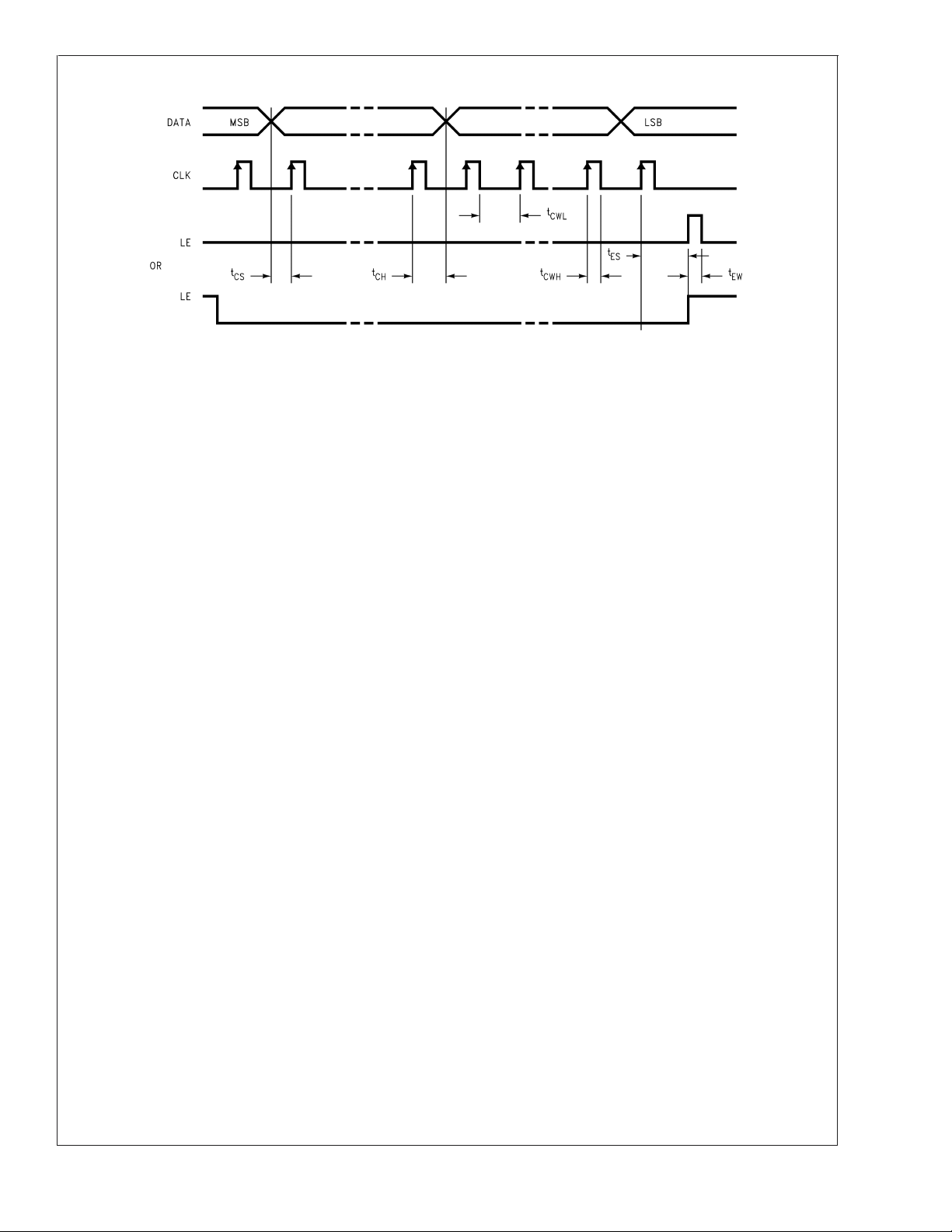
LMX243x Serial Data Input Timing
LMX2430/LMX2433/LMX2434
Notes:
1. DATA is clocked into the 24-bit shift register on the rising edge of CLK
2. The MSB of DATA is shifted in first.
20053510
www.national.com33

1.0 Functional Description
The basic phase-lock-loop (PLL) configuration consists of a
high-stability crystal reference oscillator, a frequency synthesizer such as the National Semiconductor LMX243x, a voltage controlled oscillator (VCO), and a passive loop filter. The
frequency synthesizer includes a phase detector, current
mode charge pump, programmable reference R and feedback N frequency dividers. The VCO frequency is established by dividing the crystal reference signal down via the
reference divider to obtain a comparison reference frequency. This reference signal, f
input of a phase/ frequency detector and compared with the
LMX2430/LMX2433/LMX2434
feedback signal, f
, which was obtained by dividing the VCO
p
frequency down by way of the feedback divider. The phase/
frequency detector measures the phase error between the f
and fpsignals and outputs control signals that are directly
proportional to the phase error. The charge pump then
pumps charge into or out of the loop filter based on the
magnitude and direction of the phase error. The loop filter
converts the charge into a stable control voltage for the
VCO. The phase/frequency detector’s function is to adjust
the voltage presented to the VCO until the feedback signal’s
frequency and phase match that of the reference signal.
When this “Phase-Locked” condition exists, the VCO frequency will be N times that of the comparison frequency,
where N is the feedback divider ratio.
1.1 REFERENCE OSCILLATOR INPUT
The reference oscillator frequency for both the RF and IF
PLLs is provided from an external reference via the OSCin
pin. The reference buffer circuit supports input frequencies
from 5 to 40 MHz with a minimum input sensitivity of 0.5 V
The reference buffer circuit has an approximate Vcc/2 input
threshold and can be driven from an external AC coupled
source. Typically, the OSCin pin is connected to the output of
a crystal oscillator.
1.2 REFERENCE DIVIDERS (R COUNTERS)
The reference dividers divide the reference input signal,
OSCin, by a factor of R. The output of the reference divider
circuits feeds the reference input of the phase detector. This
reference input to the phase detector is often referred to as
the comparison frequency. The divide ratio should be chosen
such that the maximum phase comparison frequency (f
PRF
or f
) of 10 MHz is not exceeded.
COMPIF
The RF and IF reference dividers are each comprised of
15-bit CMOS binary counters that support a continuous integer divide ratio from 3 to 32767. The RF and IF reference
divider circuits are clocked by the output of the reference
buffer circuit which is common to both. Refer to Sections
2.4.1 and 2.7.1 for details on how to program the RF_R and
IF_R counters.
1.3 PRESCALERS
The FinRF and FinIF input pins drive the input of a
differential-pair amplifier. The output of the differential-pair
amplifier drives a chain of D-type flip-flops in a dual modulus
configuration. The output of the prescaler is used to clock the
subsequent feedback dividers. The RF PLL complementary
inputs can be driven differentially, or the negative input can
be AC coupled to ground through an external capacitor for
single ended configuration. A 16/17 or a 32/33 prescale ratio
can be selected for the 5.0 GHz LMX2434 RF synthesizer.
An 8/9 or a 16/17 prescale ratio can be selected for both the
, is then presented to the
r
COM
LMX2430 and LMX2433 RF synthesizers. The IF PLL is
single ended. An 8/9 or a 16/17 prescale ratio can be selected for the IF synthesizer.
1.4 PROGRAMMABLE FEEDBACK DIVIDERS (N
COUNTERS)
The programmable feedback dividers operate in concert with
the prescalers to divide the input signal, Fin, by a factor of N.
The output of the programmable reference divider is provided to the feedback input of the phase detector circuit. The
divide ratio should be chosen such that the maximum phase
comparison frequency (f
COMPRF
or f
) of 10 MHz is not
COMPIF
exceeded.
r
The programmable feedback divider circuit is comprised of
an A counter (swallow counter) and a B counter (programmble binary counter). For both the LMX2430 and LMX2433,
the RF_A counter is a 4-bit swallow counter, programmable
from 0 to 15. The LMX2434 RF_A counter is a 5-bit swallow
counter, programmable from 0 to 31. The LMX243x IF_A
counter is a 4-bit swallow counter, programmable from 0 to
15. For both the LMX2430 and LMX2433, the RF_B counter
is a 15-bit binary counter, programmable from 3 to 32767.
The LMX2434 RF_B counter is a 14-bit binary counter,
programmable from 3 to 16383. The LMX243x IF_B is a
14-bit binary counter programmable from 3 to 16383. A
*
continuous integer divide ratio is achieved if N ≥ P
(P−1),
where P is the value of the prescaler selected. Divide ratios
less than the minimum continuous divide ratio are achievable as long as the binary programmable counter value is
.
PP
greater than the swallow counter value (B ≥ A). Refer to
Sections 2.5.1.1, 2.5.1.2, 2.5.2.1, 2.5.2.2, 2.8.1, and 2.8.2
for details on how to program the A and B counters. The
following equations are useful in determining and programming a particular value of N:
N=(PxB)+A
Fin=Nxf
COMP
Definitions:
f
: RF or IF phase detector comparison frequency
COMP
Fin: RF or IF input frequency
A: RF_A or IF_A counter value
-
B: RF_B or IF_B counter value
P: Preset modulus of the dual moduIus prescaler
LMX2430 RF synthesizer: P = 8 or 16
LMX2433 RF synthesizer: P = 8 or 16
LMX2434 RF synthesizer: P = 16 or 32
LMX243x IF synthesizer: P = 8 or 16
1.5 PHASE/ FREQUENCY DETECTORS
The RF and IF phase/ frequency detectors (PFD) are driven
from their respective N and R counter outputs. The maximum frequency for both the RF and IF phase detector inputs
is 10 MHz. The PFD outputs control the respective charge
pumps. The polarity of the pump-up or pump-down control
signals are programmed using the RF_CPP or IF_CPP control bits, depending on whether the RF or IF VCO characteristics are positive or negative. Refer to Sections 2.4.2 and
2.7.2 for more details. The PFDs have a detection range of
−2π to +2π. The PFDs also receive a feedback signal from
the charge pump in order to eliminate dead zone.
www.national.com 34

1.0 Functional Description (Continued)
1.5.1 Phase Comparator and Internal Charge Pump Characteristics
LMX2430/LMX2433/LMX2434
Notes:
1. The minimum width of the pump-up and pump-down current pulses occur at the CPoutRF or CPoutIF pins when the loop is phase locked.
2. The diagram assumes positive VCO characteristics, i.e. RF_CPP or IF_CPP = 1.
is the PFD input from the reference divider (R counter).
3. f
r
is the PFD input from the programmable feedback divder (N counter).
4. f
p
5. CPout refers to either the RF or IF charge pump output.
1.6 CHARGE PUMPS
The charge pump directs charge into or out of an external
loop filter. The loop filter converts the charge into a stable
control voltage which is applied to the tuning input of the
VCO. The charge pump steers the VCO control voltage
towards Vcc during pump-up events and towards GND during pump-down events. When locked, CPoutRF or CPoutIF
are primarily in a TRI-STATE mode with small corrections
occuring at the phase comparator rate. The charge pump
output current magnitude can be selected by toggling the
RF_CPG or IF_CPG control bits.
1.7 MICROWIRE SERIAL INTERFACE
The programmable register set is accessed via the MICROWIRE serial interface. A low voltage logic interface
allows direct connection to 1.8V devices. The interface is
comprised of three signal pins: CLK, DATA and LE. Serial
1.8.1 Push-Pull Analog Lock Detect Output
An analog lock detect status generated from the phase
detector is available on the Ftest/LD output pin if selected. A
push-pull configuration can be selected for the lock detect
output signal. With this configuration, the lock detect output
goes HIGH when the charge pump is inactive. It goes LOW
when the charge pump is active during a comparison cycle.
Narrow low going pulses are observed when the charge
pump turns on.
There are three separate push-pull analog lock detect signals that are routed to the multiplexer. Two of these monitor
the lock status of the individual synthesizers. The third detects the condition when both the RF and IF synthesizers are
in a locked state. External circuitry is required to provide a
steady DC signal to indicate when the PLL is in a locked
state. Refer to Section 2.10 for details on how to program
the different push-pull analog lock detect options.
data is clocked into the 24-bit shift register on the rising edge
of CLK. The last two bits decode the internal control register
address. When LE transitions HIGH, DATA stored in the shift
register is loaded into one of four control registers depending
on the state of the address bits. The MSB of DATA is loaded
in first. The synthesizers can be programmed even in power
down mode. A complete programming description is provided in Section 2.0 Programming Description.
1.8 MULTI-FUNCTION OUTPUTS
The LMX243x device’s Ftest/LD output pin is a multi-function
output that can be configured as a general purpose CMOS
TRI-STATE output, push-pull analog lock detect output,
open-drain analog lock detect output, digital filtered lock
detect output, or used to monitor the output of the various
reference divider (R counter) or feedback divider (N counter)
circuits. The Ftest/LD control word is used to select the
1.8.2 Open-Drain Analog Lock Detect Output
The lock detect output can be an open-drain configuration. In
this configuration, the lock detect output goes to a high
impedance state when the charge pump is inactive. It goes
LOW when the charge pump is active during a comparison
cycle. When a pull-up resistor is used, narrow low going
pulses are observed when the charge pump turns on.
Similarly, three separate open-drain analog lock detect sig-
nals are routed to the multiplexer. Two of these monitor the
lock status of the individual synthesizers. The third detects
the condition when both the RF and IF synthesizers are in a
locked state. External circuitry is required to provide a steady
DC signal to indicate when the PLL is in a locked state. Refer
to Section 2.10 for details on how to program the different
open-drain analog lock detect options.
desired output function. When the PLL is in powerdown
mode, the Ftest/LD output is disabled and is in a high
impedance state. A complete programming description of the
multi-function output is provided in Section 2.10.
20053511
www.national.com35

1.0 Functional Description (Continued)
1.8.3 Digital Filtered Lock Detect Output
A digital filtered lock detect status generated from the phase
detector is also available on the Ftest/LD output pin if selected. The lock detect digital filter compares the difference
bewteen the phases of the inputs to the PFD to an RC
generated delay of approximately 15 ns. If the phase error is
less than the 15 ns RC delay for 5 consecutive reference
LMX2430/LMX2433/LMX2434
cycles, the PLL enters a locked state (HIGH). Once in lock,
the RC delay is changed to approximately 30 ns. Once the
phase error becomes greater than the 30 ns RC delay, the
PLL falls out of lock (LOW). When the PLL is in powerdown
mode, the Ftest/LD output is forced LOW. A flow chart of the
digital filtered lock detect output is shown below.
Similarly, three separate digital filtered lock detect signals
are routed to the multiplexer. Two of these monitor the lock
status of the individual synthesizers. The third detects the
condition when both the RF and IF synthesizers are in a
www.national.com 36
20053503
locked state. External circuitry is not required when the
digital filtered lock detect option is selected. Refer to Section
2.10 for details on how to program the different digital filtered
lock detect options.

1.0 Functional Description (Continued)
1.8.4 Reference Divider and Feedback Divider Output
The outputs of the various N and R dividers can be monitored by selecting the appropriate Ftest/LD word. This is
essential when performing OSCin or Fin sensitivity measurements. Refer to the LMX243x FinRF Sensitivity Test Setup
or LMX243x OSCin Sensitivity Test Setup sections for
more details. Note, the R and N outputs that are routed to
the Ftest/LD are R/2 and N/2 respectively. The internal /2
circuit is used to provide a 50% duty cycle. Refer to Section
2.10 for more details on how to route the appropriate divider
output to the Ftest/LD pin.
1.9 FASTLOCK OUTPUT
The LMX243x Fastlock feature allows a faster loop response
time during lock aquisition. The loop response time (lock
time) can be approximately halved if the loop bandwidth is
doubled. In order to achieve this, the same gain/ phase
relationship should be maintained when the loop bandwidth
is doubled. When the FLoutRF or OSCout/ FLoutIF pins are
configured as FastLock outputs, an open drain device is
enabled. The open drain device switches in a resistor parallel, and of equal value, to R2 of the external loop filter. The
loop bandwidth is effectively doubled and stability is maintained. Once locked to the correct frequency, the PLL will
return to a steady state condition.The LMX243x offers two
methods to achieve Fastlock: manual and automatic.
Manual Fastlock is achieved by increasing the charge pump
current from 1 mA (RF_CPG/ IF_CPG Bit = 0) in the steady
state mode, to 4 mA (RF_CPG/ IF_CPG Bit = 1) in Fastlock
mode. Automatic Fastlock is achieved by programming the
timeout counter register (RF_TOC/ IF_TOC) with the appropriate number of phase comparison cycles that the RF/ IF
synthesizer will spend in the Fastlock state. Refer to Sec-
tions 2.6 and 2.9 for details on how to configure the
FLoutRF or OSCout/ FLoutIF output to an open drain Fastlock output.
be enabled if the ENosc pin is set HIGH, independent of the
state of the EN pin. This capability allows the oscillator buffer
to be used as a crystal oscillator. When EN is set HIGH,
powerdown is controlled through the MICROWIRE. The
powerdown word is comprised of the RF_PD/ IF_PD bit, in
conjuction with the RF_CPT/ IF_CPT bit. The powerdown
control word is used to set the operating mode of the device.
Refer to Sections 2.4.4, 2.5.4, 2.7.4, and 2.8.4 for details on
how to program the RF or IF powerdown bits.
When either synthesizer is powered down, the respective
prescaler, phase detector, and charge pump circuit is dis-
abled. The CPoutRF/ CPoutIF, FinRF/ FinIF, and FinRF
pins are all forced to a high impedance state. The reference
divider and feedback divider circuits are held at the load
point during powerdown. The oscillator buffer is disabled
when the ENosc pin is set LOW. The OSCin pin is forced to
a HIGH state through an approximate 100 kΩ resistance
when this condition exists. When either synthesizer is acti-
vated, the respective prescaler, phase detector, charge
pump circuit, and the oscillator buffer are all powered up.
The feedback divider and reference divider are held at their
load point. This allows the reference oscillator, feedback
divider, reference divider and prescaler circuitry to reach
proper bias levels. After a finite delay, the feedback and
reference dividers are enabled and they resume counting in
close alignment (the maximum error is one prescaler cycle).
The MICROWIRE control register remains active and ca-
pable of loading and latching data while in powerdown
mode.
1.11.1 Synchronous Powerdown Mode
In this mode, the powerdown function is gated by the charge
pump. When the device is configured for synchronous pow-
erdown, the device will enter the powerdown mode upon
completion of the next charge pump pulse event.
LMX2430/LMX2433/LMX2434
*
1.10 COUNTER RESET
When the RF_RST/ IF_RST bit is enabled, both the feedback divider (RF_N/ IF_N) and reference divider (RF_R/
IF_R) are held at their load point. When the device is programmed to normal operation, both the feedback divider and
reference divder are enabled and resume counting in close
alignment to each other. Refer to Sections 2.4.5 and 2.7.5
for more details.
1.11 POWER CONTROL
The LMX243x device can be asynchronously powered down
when the EN pin is set LOW, independent of the state of the
powerdown bits. Note that the OSCout/ FLoutIF pin can still
EN Pin RF_CPT/
IF_CPT Bit
0 X X Asynchronous Powerdown
1 0 0 PLL Active.
1 1 0 PLL Active.
1 0 1 Synchronous Powerdown
1 1 1 Asynchronous Powerdown
Note: X refers to a don’t care condition.
RF_PD/
IF_PD Bit
1.11.2 Asynchronous Powerdown Mode
In this mode, the powerdown function is NOT gated by the
completion of a charge pump pulse event. When the device
is configured for asynchronous powerdown, the part will go
into powerdown mode immediately.
Normal Operation
Charge Pump Output in High Impedance State
Operating Mode
www.national.com37

2.0 Programming Description
2.1 MICROWIRE INTERFACE
The 24-bit shift register is loaded via the MICROWIRE interface. The shift register consists of a 21-bit DATA[20:0] FIELD and a
3-bit ADDRESS[2:0] FIELD as shown below. The ADDRESS FIELD is used to decode the internal control register address. When
LE transitions HIGH, DATA stored in the shift register is loaded into one of 6 control registers depending on the state of the
ADDRESS bits. The MSB of DATA is loaded into the shift register first. The DATA FIELD assignments are shown in Section 2.3
CONTROL REGISTER CONTENT MAP.
MSB LSB
DATA[20:0] ADDRESS[2:0]
LMX2430/LMX2433/LMX2434
2.2 CONTROL REGISTER LOCATION
The ADDRESS[2:0] bits decode the internal register address. The table below shows how the ADDRESS bits are mapped into
the target control register.
23 3 2 0
ADDRESS[2:0] Target
FIELD Register
000 R0
001 R1
010 R2
011 R3
100 R4
101 R5
2.3 CONTROL REGISTER CONTENT MAP
The control register content map describes how the bits within each control register are allocated to specific control functions. The
bits that are marked 0 should be programmed as such to ensure proper device operation.
Reg23222120191817161514131211109876543210
DATA[20:0] FIELD
RF_
RF_
RF_
R0 MUX[3:2]
RF_PDRF_
R1
RF_PDRF_
R1
R2 000000000 RF_TOC[11:0] 0 1 0
R3 MUX[1:0]
IF_PDIF_
R4
R5 000000000 IF_TOC[11:0] 1 0 1
RST
CPT
P
P
IF_
IF_
RST
CPT
0 IF_B[13:0] IF_A[3:0] 1 0 0
P
CPG
IF_
CPG
RF_
CPP
IF_
CPP
LMX2430/33
RF_B[14:0]
LMX2434
RF_B[13:0]
RF_R[14:0] 0 0 0
LMX2430/33
RF_A[3:0]
LMX2434
RF_A[4:0]
IF_R[14:0] 0 1 1
ADDRESS
[2:0]
FIELD
001
001
www.national.com 38

2.0 Programming Description (Continued)
2.4 R0 REGISTER
The R0 register contains the RF_R, RF_CPP, RF_CPG, RF_CPT, and RF_RST control words, in addition to two of the four bits
that compose the MUX control word. The detailed descriptions and programming information for each control word is discussed
in the following sections.
Reg23222120191817161514131211109876543210
DATA[20:0] FIELD
RF_
RF_
RF_
R0 MUX[3:2]
RST
CPT
CPG
RF_
CPP
RF_R[14:0] 0 0 0
2.4.1 RF_R[14:0] - RF Synthesizer Programmable Reference Divider (R Counter) (R0[17:3])
The RF reference divider (RF_R) can be programmed to support divide ratios from 3 to 32767. Divide ratios less than 3 are
prohibited.
Divide Ratio RF_R[14:0]
14131211109876543210
3 000000000000011
4 000000000000100
• •••••••••••••••
32767 111111111111111
2.4.2 RF_CPP - RF Synthesizer Phase Detector Polarity (R0[18])
The RF_CPP bit is used to control the RF synthesizer’s phase/ frequency detector polarity based on the VCO tuning
characteristics.
Control Bit Register Location Description Function
01
RF_CPP R0[18] RF Phase/
Frequency Detector
Polarity
RF VCO Negative
Tuning
Characteristics
RF VCO Positive
Tuning
Characteristics
RF VCO Characteristics
ADDRESS
[2:0]
FIELD
LMX2430/LMX2433/LMX2434
20053567
www.national.com39

2.0 Programming Description (Continued)
2.4.3 RF_CPG - RF Synthesizer Charge Pump Current Gain (R0[19])
The RF_CPG bit controls the RF synthesizer’s charge pump gain. Two gain levels are available.
Control Bit Register Location Description Function
01
RF_CPG R0[19] RF Charge Pump
Current Gain
2.4.4 RF_CPT - RF Synthesizer Charge Pump TRI-STATE (R0[20])
LMX2430/LMX2433/LMX2434
The RF_CPT bit allows the charge pump to be switched between a normal operating mode and a high impedance output state.
This happens asynchronously with the change in the RF_CPT bit.
Furthermore, the RF_CPT bit operates in conjuction with the RF_PD bit to set a synchronous or an asynchronous powerdown
mode. Refer to Section 2.5.4 for more details on how to program the RF_PD bit.
Control Bit Register Location Description Function
RF_CPT R0[20] RF Charge Pump
TRI-STATE
RF Charge Pump
Normal Operation
2.4.5 RF_RST - RF Synthesizer Counter Reset (R0[21])
The RF_RST bit resets the RF_A, RF_B and RF_R counters. After removing the reset, the RF_A and RF_B counters resume
counting in close alignment with the RF_R counter. The maximum error is one prescaler cycle.
Control Bit Register Location Description Function
RF_RST R0[21] RF Counter Reset RF_A, RF_B and
RF_R
Normal Operation
LOW
1mA
HIGH
4mA
01
RF Charge Pump
Output in High
Impedance State
01
RF_A, RF_B and
RF_R
Reset
2.5 R1 REGISTER
The R1 register contains the RF_A, RF_B, RF_P, and RF_PD control words. The RF_A and RF_B control words are used to setup
the programmable feedback divider. The detailed descriptions and programming information for each control word is discussed
in the following sections.
Reg23222120191817161514131211109876543210
ADDRESS
[2:0]
FIELD
001
001
R1
R1
RF_PDRF_
P
RF_PDRF_
P
DATA[20:0] FIELD
LMX2430/33
RF_B[14:0]
LMX2434
RF_B[13:0]
LMX2430/33
RF_A[3:0]
LMX2434
RF_A[4:0]
2.5.1 LMX243x RF Synthesizer Swallow Counter
2.5.1.1 RF_A[3:0] - LMX2430/33 RF Synthesizer Swallow Counter (A Counter) (R1[6:3])
The RF_A control word is used to setup the RF synthesizer’s A counter. For both the LMX2430 and LMX2433, the A counter is
a 4-bit swallow counter used in the programmable feedback divider. The RF_A control word can be programmed to values ranging
from 0 to 15.
Divide Ratio LMX2430/33
RF_A[3:0]
321 0
0000 0
1000 1
•••• •
15111 1
www.national.com 40

2.0 Programming Description (Continued)
2.5.1.2 RF_A[4:0] - LMX2434 RF Synthesizer Swallow Counter (A Counter) (R1[7:3])
The LMX2434 A counter is a 5-bit swallow counter used in the programmable feedback divider. The RF_A control word can be
programmed to values ranging from 0 to 31.
Divide Ratio LMX2434
RF_A[4:0]
43210
000000
100001
••••••
3111111
2.5.2 LMX243x RF Synthesizer Programmable Binary Counter
2.5.2.1 RF_B[14:0] - LMX2430/33 RF Synthesizer Programmable Binary Counter (B Counter) (R1[21:7])
The RF_B control word is used to setup the RF synthesizer’s B counter. For both the LMX2430 and LMX2433, the B counter is
a 15-bit programmable binary counter used in the programmable feedback divider. The RF_B control word can be programmed
to values ranging from 3 to 32767. Divide ratios less than 3 are prohibited.
Divide
Ratio
14131211109876543210
3000000000000011
4000000000000100
••••••••••••••••
32767 111111111111111
LMX2430/33
RF_B[14:0]
LMX2430/LMX2433/LMX2434
2.5.2.2 RF_B[13:0] - LMX2434 RF Synthesizer Programmable Binary Counter (B Counter) (R1[21:8])
The LMX2434 B counter is a 14-bit programmable binary counter used in the programmable feedback divider. The RF_B control
word can be programmed to values ranging from 3 to 16383. Divide ratios less than 3 are prohibited.
Divide
Ratio
131211109876543210
300000000000011
400000000000100
LMX2434
RF_B[13:0]
•••••••••••••••
16383 11111111111111
2.5.3 LMX243x RF Synthesizer Prescaler Select
2.5.3.1 RF_P - LMX2430/33 RF Synthesizer Prescaler Select (R1[22])
Both the LMX2430 and LMX2433 RF synthesizers utilize a selectable dual modulus prescaler. An 8/9 or a 16/17 prescale ratio
can be selected.
Control Bit Register Location Description Function
01
RF_P R1[22] LMX2430/33
RF Prescaler Select
2.5.3.2 RF_P - LMX2434 RF Synthesizer Prescaler Select (R1[22])
The LMX2434 RF synthesizer utilizes a selectable dual modulus prescaler. A 16/17 or a 32/33 prescale ratio can be selected.
Control Bit Register Location Description Function
RF_P R1[22] LMX2434
RF Prescaler Select
8/9 Prescaler
Selected
01
16/17 Prescaler
Selected
16/17 Prescaler
Selected
32/33 Prescaler
Selected
www.national.com41

2.0 Programming Description (Continued)
2.5.4 RF_PD - RF Synthesizer Powerdown (R1[23])
The RF_PD bit is used to switch the RF PLL between a powered up and powered down mode.
Furthermore, the RF_PD bit operates in conjuction with the RF_CPT bit to set a synchronous or an asynchronous powerdown
mode. Refer to Section 2.4.4 for more details on how to program the RF_CPT bit.
Control Bit Register Location Description Function
01
RF_PD R1[23] RF Powerdown RF PLL Active RF PLL Powerdown
LMX2430/LMX2433/LMX2434
2.6 R2 REGISTER
The R2 Register contains the RF_TOC control word. The RF_TOC is used to setup the RF syhnthesizer’s Fastlock circuitry. The
RF_TOC is a 12-bit binary counter programmable from 0 to 4095.
Reg23222120191817161514131211109876543210
DATA[20:0] FIELD
R2 000000000 RF_TOC[11:0] 0 1 0
2.6.1 RF_TOC[0:11] - RF Synthesizer Timeout Counter (R2[14:3])
The FLoutRF pin can be configured as a general purpose CMOS TRI-STATE output or as a Fastlock output by programming the
RF_TOC appropriately. When the RF_TOC is programmed from 0 to 3, Automatic Fastlock is disabled, and the FLoutRF pin is
either configured as a general purpose CMOS TRI-STATE output or Manual Fastlock is enabled. When the RF_TOC is
programmed to 0, the FLoutRF pin will be in TRI-STATE (high impedance) mode. The charge pump current is then the value
specified by RF_CPG (R0[19]). When the RF_TOC is programmed to 1, the FLoutRF pin is pulled to a LOW state. The charge
pump current is then set to a HIGH gain state (RF_CPG bit = 1). This condition is known as the Manual Fastlock. When the
RF_TOC is programmed to 2, the FLout_RF pin will again be pulled to a LOW state, but this time the charge pump current is the
value specified by RF_CPG (R0[19]). When the RF_TOC is programmed to 3, the FLoutRF pin is pulled to a HIGH state. Again,
the charge pump current is the value specified by RF_CPG (R0[19]). When the RF_TOC is programmed from 4 to 4095, Fastlock
is enabled and the FLoutRF pin is pulled to a LOW state. Fastlock will time-out after the specified number of PFD events. At this
time, the FLoutRF pin will switch to TRI-STATE (high impedance) mode. The value programmed into RF_TOC represents the
number of PFD events that the RF synthesizer will spend in the Fastlock state. Note that any write to the RF_TOC requires a PFD
event on the RF synthesizer to latch the contents. This means that writes to the RF_TOC take effect synchronously with the next
PFD event.
RF_TOC[11:0] FastLock Mode Fastlock Period
[PFD Events]
0 Disabled N/A General Purpose.
1 Enabled
N/A General Purpose.
Manual Fastlock
2 Disabled N/A General Purpose.
3 Disabled N/A General Purpose.
4 Enabled
4 FastLock.
Automatic Fastlock
FLoutRF Pin
Functionality/ State
High Impedance State
Logic LOW State
Logic LOW State
Logic HIGH State
Logic LOW State.
Switches to High
I
CPoutRF
I
CPoutRF
controlled by R0[19]
I
CPoutRF
I
CPoutRF
controlled by R0[19]
I
CPoutRF
controlled by R0[19]
I
CPoutRF
Switches to 1 mA after
4 PFD events
Impedance after 4 PFD
events
……………
4095 Enabled
Automatic Fastlock
4095 FastLock.
Logic LOW State.
Switches to High
I
CPoutRF
Switches to 1 mA after
4095 PFD events
Impedance after 4095
PFD events
ADDRESS
Magnitude
magnitude
=4mA
magnitude
magnitude
=4mA
=4mA
[2:0]
FIELD
www.national.com 42

2.0 Programming Description (Continued)
2.7 R3 REGISTER
The R3 register contains the IF_R, IF_CPP, IF_CPG, IF_CPT, and IF_RST control words, in addition to two of the four bits that
compose the MUX control word. The detailed descriptions and programming information for each control word is discussed in the
following sections.
Reg23222120191817161514131211109876543210
DATA[20:0] FIELD
IF_
IF_
IF_
R3 MUX[1:0]
RST
CPT
CPG
IF_
CPP
IF_R[14:0] 0 1 1
2.7.1 IF_R[14:0] - IF Synthesizer Programmable Reference Divider (R Counter) (R3[17:3])
The IF reference divider (IF_R) can be programmed to support divide ratios from 3 to 32767. Divide ratios less than 3 are
prohibited.
Divide Ratio IF_R[14:0]
14131211109876543210
3 000000000000011
4 000000000000100
• •••••••••••••••
32767 111111111111111
2.7.2 IF_CPP - IF Synthesizer Phase Detector Polarity (R3[18])
The IF_CPP bit is used to control the IF synthesizer’s phase/ frequency detector polarity based on the VCO tuning characteristics.
Control Bit Register Location Description Function
01
IF_CPP R3[18] IF Phase/ Frequency
Detector Polarity
IF VCO Negative
Tuning
Characteristics
IF VCO Positive
Tuning
Characteristics
IF VCO Characteristics
ADDRESS
[2:0]
FIELD
LMX2430/LMX2433/LMX2434
20053568
www.national.com43

2.0 Programming Description (Continued)
2.7.3 IF_CPG - IF Synthesizer Charge Pump Current Gain (R3[19])
The IF_CPG bit controls the IF synthesizer’s charge pump gain. Two gain levels are available.
Control Bit Register Location Description Function
01
IF_CPG R3[19] IF Charge Pump
Current Gain
2.7.4 IF_CPT - IF Synthesizer Charge Pump TRI-STATE (R3[20])
LMX2430/LMX2433/LMX2434
The IF_CPT bit allows the charge pump to be switched between a normal operating mode and a high impedance output state.
This happens asynchronously with the change in the IF_CPT bit.
Furthermore, the IF_CPT bit operates in conjuction with the IF_PD bit to set a synchronous or an asynchronous powerdown
mode. Refer to Section 2.8.4 for more details on how to program the IF_PD bit.
Control Bit Register Location Description Function
IF_CPT R3[20] IF Charge Pump
TRI-STATE
IF Charge Pump
Normal Operation
2.7.5 IF_RST - IF Synthesizer Counter Reset (R3[21])
The IF_RST bit resets of the IF_A, IF_B and IF_R counters. After removing the reset, the IF_A and IF_B counters resume
counting in close alignment with the IF_R counter. The maximum error is one prescaler cycle.
Control Bit Register Location Description Function
IF_RST R3[21] IF Counter Reset IF_A, IF_B and IF_R
Normal Operation
LOW
1mA
HIGH
4mA
01
IF Charge Pump
Output in High
Impedance State
01
IF_A, IF_B and IF_R
Reset
2.8 R4 REGISTER
The R4 register contains the IF_A, IF_B, IF_P, and IF_PD control words. The IF_A and IF_B control words are used to setup the
programmable feedback divider. The detailed descriptions and programming information for each control word is discussed in the
following sections. R4[21] is always set to 0.
Reg23222120191817161514131211109876543210
ADDRESS
[2:0]
FIELD
R4
IF_PDIF_
DATA[20:0] FIELD
0 IF_B[13:0] IF_A[3:0] 1 0 0
P
2.8.1 IF_A[3:0] - IF Synthesizer Swallow Counter (A Counter) (R4[6:3])
The IF_A control word is used to setup the IF synthesizer’s A counter. The A counter is a 4-bit swallow counter used in the
programmable feedback divider. The IF_A control word can be programmed to values ranging from 0 to 15.
Divide Ratio IF_A[3:0]
321 0
0000 0
1000 1
•••• •
15111 1
www.national.com 44
2.0 Programming Description (Continued)
2.8.2 IF_B[13:0] - IF Synthesizer Programmable Binary Counter (B Counter) (R4[20:7])
The IF_B control word is used to setup the IF synthesizer’s B counter. The B counter is a 14-bit programmable binary counter
used in the programmable feedback divider. The IF_B control word can be programmed to values ranging from 3 to 16383. Divide
ratios less than 3 are prohibited.
Divide
Ratio
131211109876543210
300000000000011
400000000000100
•••••••••••••••
16383 11111111111111
2.8.3 IF_P - IF Synthesizer Prescaler Select (R4[22])
The LMX243x IF synthesizer utilizes a selectable dual modulus prescaler. An 8/9 or a 16/17 prescale ratio can be selected.
Control Bit Register Location Description Function
IF_P R4[22] IF Prescaler Select 8/9 Prescaler
2.8.4 IF_PD - IF Synthesizer Powerdown (R4[23])
The IF_PD bit is used to switch the IF PLL between a powered up and powered down mode.
Furthermore, the IF_PD bit operates in conjuction with the IF_CPT bit to set a synchronous or an asynchronous powerdown
mode. Refer to Section 2.7.4 for more details on how to program the IF_CPT bit.
Control Bit Register Location Description Function
IF_PD R4[23] IF Powerdown IF PLL Active IF PLL Powerdown
IF_B[13:0]
Selected
01
16/17 Prescaler
Selected
01
LMX2430/LMX2433/LMX2434
www.national.com45

2.0 Programming Description (Continued)
2.9 R5 REGISTER
The R5 Register contains the IF_TOC control word. The IF_TOC is used to setup the IF syhnthesizer’s Fastlock circuitry. The
IF_TOC is a 12-bit binary counter programmable from 0 to 4095.
Reg23222120191817161514131211109876543210
DATA[20:0] FIELD
R5 000000000 IF_TOC[11:0] 1 0 1
2.9.1 IF_TOC[0:11] - IF Synthesizer Timeout Counter (R5[14:3])
LMX2430/LMX2433/LMX2434
The OSCout/ FLoutIF pin can be configured as a general purpose CMOS TRI-STATE output or as a Fastlock output by
programming the IF_TOC appropriately. When the IF_TOC is programmed from 0 to 3, Automatic Fastlock is disabled, and the
OSCout/ FLoutIF pin is configured as a general purpose CMOS TRI-STATE output or Manual Fastlock is enabled. When the
IF_TOC is programmed to 0, the OSCout/ FLoutIF pin will be in TRI-STATE (high impedance) mode. The charge pump current
is then the value specified by IF_CPG (R3[19]). When the IF_TOC is programmed to 1, the OSCout/ FLoutIF pin is pulled to a
LOW state. The charge pump current is then set to a HIGH gain state (IF_CPG bit = 1). This condition is known as the Manual
Fastlock. When the IF_TOC is programmed to 2, the OSCout/ FLout_IF pin will again be pulled to a LOW state, but this time the
charge pump current is the value specified by IF_CPG (R3[19]). When the IF_TOC is programmed to 3, the OSCout/ FLoutIF pin
is pulled to a HIGH state. Again, the charge pump current is the value specified by IF_CPG (R3[19]). When the IF_TOC is
programmed from 4 to 4095, Fastlock is enabled and the OSCout/ FLoutIF pin is pulled to a LOW state. Fastlock will time-out after
the specified number of PFD events. At this time, the OSCout/ FLoutIF pin will switch to TRI-STATE (high impedance) mode. The
value programmed into IF_TOC represents the number of PFD events that the IF synthesizer will spend in the Fastlock state.
Note that any write to the IF_TOC requires a PFD event on the IF synthesizer to latch the contents. This means that writes to the
IF_TOC take effect synchronously with the next PFD event.
IF_TOC[11:0] FastLock Mode Fastlock Period
[PFD Events]
0 Disabled N/A General Purpose.
1 Enabled
N/A General Purpose.
Manual Fastlock
2 Disabled N/A General Purpose.
3 Disabled N/A General Purpose.
4 Enabled
4 FastLock.
Automatic Fastlock
OSCout/ FLoutIF Pin
Functionality/ State
High Impedance State
Logic LOW State
Logic LOW State
Logic HIGH State
Logic LOW State.
Switches to High
I
CPoutIF
I
CPoutIF
controlled by R3[19]
I
CPoutIF
I
CPoutIF
controlled by R3[19]
I
CPoutIF
controlled by R3[19]
I
CPoutIF
Switches to 1 mA after
4 PFD events
Impedance after 4 PFD
events
……………
4095 Enabled
Automatic Fastlock
4095 FastLock.
Logic LOW State.
Switches to High
I
CPoutIF
Switches to 1 mA after
4095 PFD events
Impedance after 4095
PFD events
ADDRESS
Magnitude
magnitude
=4mA
magnitude
magnitude
=4mA
=4mA
[2:0]
FIELD
www.national.com 46
2.0 Programming Description (Continued)
2.10 MUX[3:0] - MULTIFUNCTION OUTPUT SELECT (R3[23:22]:R0[23:22])
The MUX control word is used to determine which signal is routed to the Ftest/LD pin.
MUX[3:0] MUX Output State
0 0 0 0 High Impedance (TRI-STATE) State Output
0 0 0 1 Logic HIGH State Output
0 0 1 0 Logic LOW State Output
0011
0100
0101
0110
0111
1000
1001
1010
1011
1 1 0 0 IF_R/ 2 Frequency
1 1 0 1 IF_N/ 2 Frequency
1 1 1 0 RF_R/ 2 Frequency
1 1 1 1 RF_N/ 2 Frequency
RF PLL and IF PLL Digital Lock Detect.
Open Drain Output
RF PLL Digital Lock Detect.
Open Drain Output
IF PLL Digital Lock Detect.
Open Drain Output
RF PLL and IF PLL Analog Lock Detect.
Open Drain Output
RF PLL Analog Lock Detect.
Open Drain Output
IF PLL Analog Lock Detect.
Open Drain Output
RF PLL and IF PLL Analog Lock Detect.
Push-Pull Output
RF PLL Analog Lock Detect.
Push-Pull Output
IF PLL Analog Lock Detect.
Push-Pull Output
LMX2430/LMX2433/LMX2434
Notes:
1. RF_N = (RF_B
2. IF_N = (IF_B
*
RF_P) + RF_A
*
IF_P) + IF_A
www.national.com47
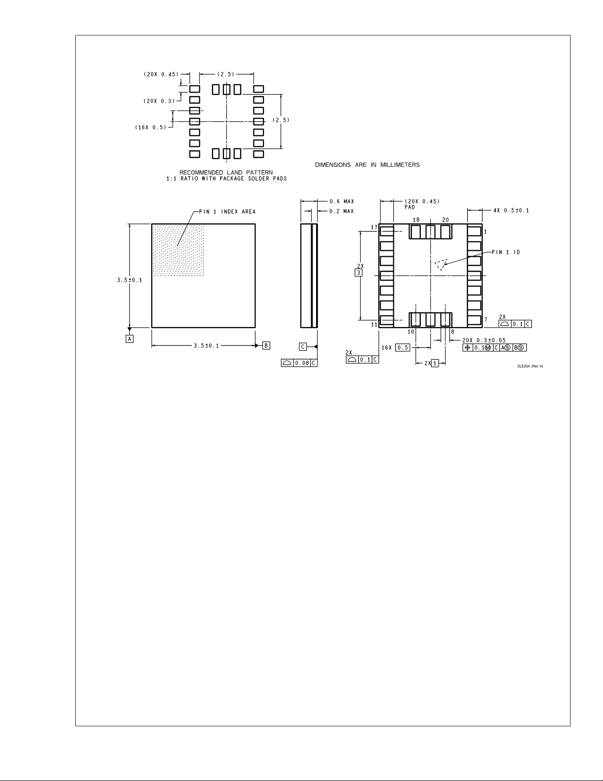
Physical Dimensions inches (millimeters) unless otherwise noted
LMX2430/LMX2433/LMX2434
20-Pin Ultra Thin Chip Scale Package (UTCSP)
NS Package Number SLE20A
www.national.com 48
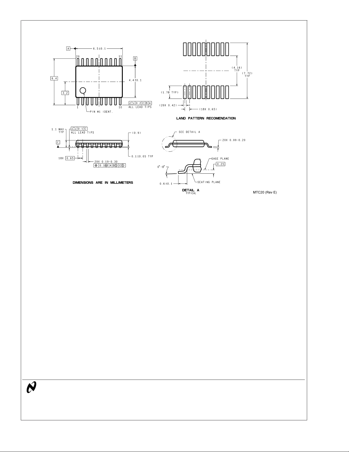
Physical Dimensions inches (millimeters) unless otherwise noted (Continued)
LMX2430/LMX2433/LMX2434 PLLatinum Dual High Frequency Synthesizer for RF Personal
Communications
20-Pin Thin Shrink Small Outine Package (TSSOP)
NS Package Number MTC20
LIFE SUPPORT POLICY
NATIONAL’S PRODUCTS ARE NOT AUTHORIZED FOR USE AS CRITICAL COMPONENTS IN LIFE SUPPORT
DEVICES OR SYSTEMS WITHOUT THE EXPRESS WRITTEN APPROVAL OF THE PRESIDENT AND GENERAL
COUNSEL OF NATIONAL SEMICONDUCTOR CORPORATION. As used herein:
1. Life support devices or systems are devices or
systems which, (a) are intended for surgical implant
into the body, or (b) support or sustain life, and
whose failure to perform when properly used in
accordance with instructions for use provided in the
2. A critical component is any component of a life
support device or system whose failure to perform
can be reasonably expected to cause the failure of
the life support device or system, or to affect its
safety or effectiveness.
labeling, can be reasonably expected to result in a
significant injury to the user.
National Semiconductor
Americas Customer
Support Center
Email: new.feedback@nsc.com
Tel: 1-800-272-9959
www.national.com
National does not assume any responsibility for use of any circuitry described, no circuit patent licenses are implied and National reserves the right at any time without notice to change said circuitry and specifications.
National Semiconductor
Europe Customer Support Center
Fax: +49 (0) 180-530 85 86
Email: europe.support@nsc.com
Deutsch Tel: +49 (0) 69 9508 6208
English Tel: +44 (0) 870 24 0 2171
Français Tel: +33 (0) 1 41 91 8790
National Semiconductor
Asia Pacific Customer
Support Center
Email: ap.support@nsc.com
National Semiconductor
Japan Customer Support Center
Fax: 81-3-5639-7507
Email: jpn.feedback@nsc.com
Tel: 81-3-5639-7560
 Loading...