

查询LMX2350供应商
LMX2350/LMX2352 PLLatinumTM Fractional N RF / Integer N IF Dual Low Power Frequency
Synthesizer
LMX2350/LMX2352
PLLatinum
™
Fractional N RF / Integer N IF
Dual Low Power Frequency Synthesizer
LMX2350 2.5 GHz/550 MHz
LMX2352 1.2 GHz/550 MHz
General Description
The LMX2350/2352 is part of a family of monolithic integrated fractional N/ Integer N frequency synthesizers designed to be used in a local oscillator subsystem for a radio
transceiver. It is fabricated using National’s 0.5µ ABiC V silicon BiCMOS process. The LMX2350/2352 contains dual
modulus prescalers along with modulo 15 or 16 fractional
compensation circuitry in the RF divider. A 16/17 or 32/33
prescale ratio can be selected for the LMX2350, and the
LMX2352 provides 8/9 or 16/17 prescale ratios. The IF circuitry for both the LMX2350 and LMX2352 contains an 8/9
prescaler, and is fully programmable. Using a fractional N
phase locked loop technique, the LMX2350 /52 can generate very stable low noise control signals for UHF and VHF
voltage controlled oscillators (VCO’s).
For the RF PLL, a highly flexible 16 level programmable
charge pump supplies output current magnitudes from
100µA to 1.6mA. Two uncommitted CMOS outputs can be
used to provide external control signals, or configured to
™
FastLock
LMX2350/2352 via a three wire interface (Data, LE, Clock).
Supply voltage can range from 2.7 V to 5.5 V.TheLMX2350/
mode. Serial data is transferred into the
2352 family features very low current consumption; typically
LMX2350 (2.5 GHz) 6.75 mA, LMX2352 (1.2 GHz) 5.00 mA
at 3.0V.TheLMX2350/2352areavailablein a 24-pin TSSOP
surface mount plastic package.
Features
n 2.7 V to 5.5 V operation
n Low current consumption
LMX2350: Icc = 6.75mA typ at 3v
LMX2352: Icc = 5.00mA typ at 3v
n Programmable or logical power down mode
Icc=5µAtypat3v
n Modulo 15 or 16 fractional RF N divider supports ratios
of 1, 2, 3, 4, 5, 8, 15, or 16
n Programmable charge pump current levels
RF 100µA to 1.6mA in 100µA steps
IF 100µA or 800 µA
n Digital filtered lock detect
Applications
n Portable wireless communications (PCS/PCN, cordless)
n Dual mode cellular telephone systems
n Zero blind slot TDMA systems
n Spread spectrum communication systems (CDMA)
n Cable TV Tuners (CATV)
PRELIMINARY
June 1999
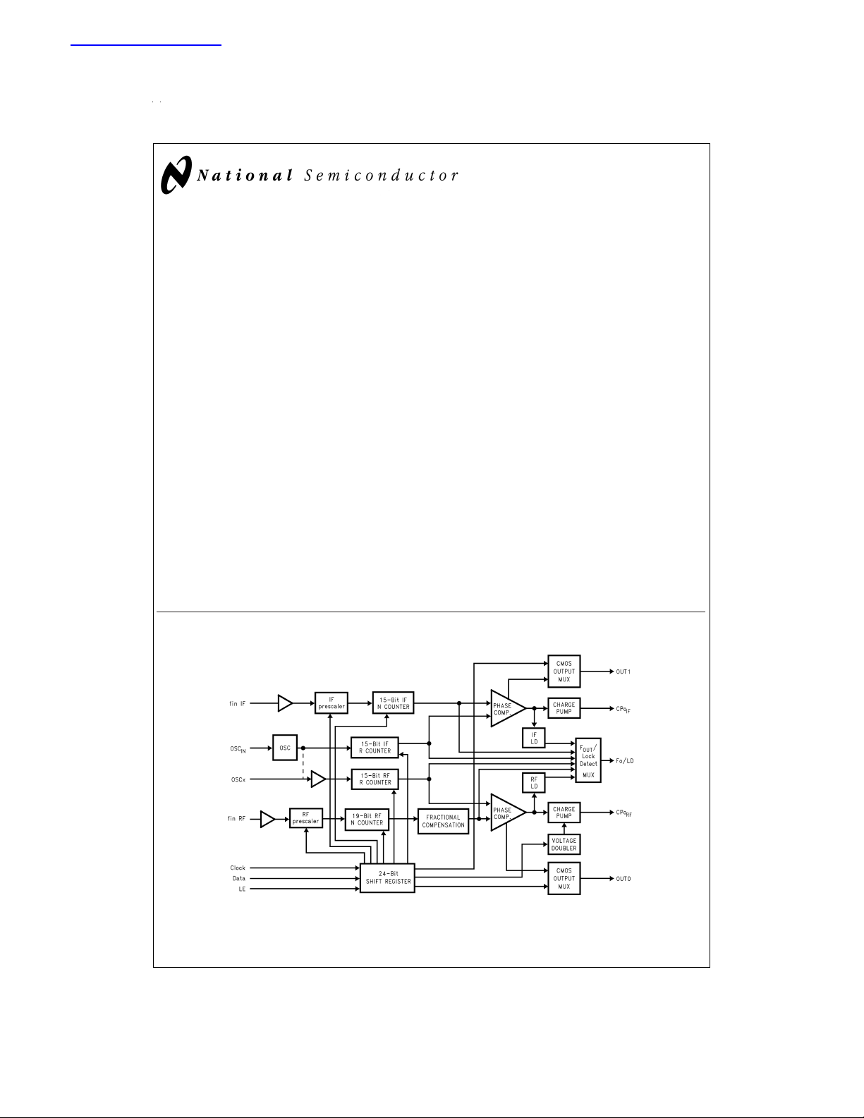
Block Diagram
DS100831-1
FastLock™is a trademark of National Semiconductor Corporation.
™
MICROWIRE
PLLatinum
TRI-STATE
© 1999 National Semiconductor Corporation DS100831 www.national.com
is a trademark of National Semiconductor Corporation.
™
is a trademark of National Semiconductor Corporation.
®
is a registered trademark of National Semiconductor Corporation.
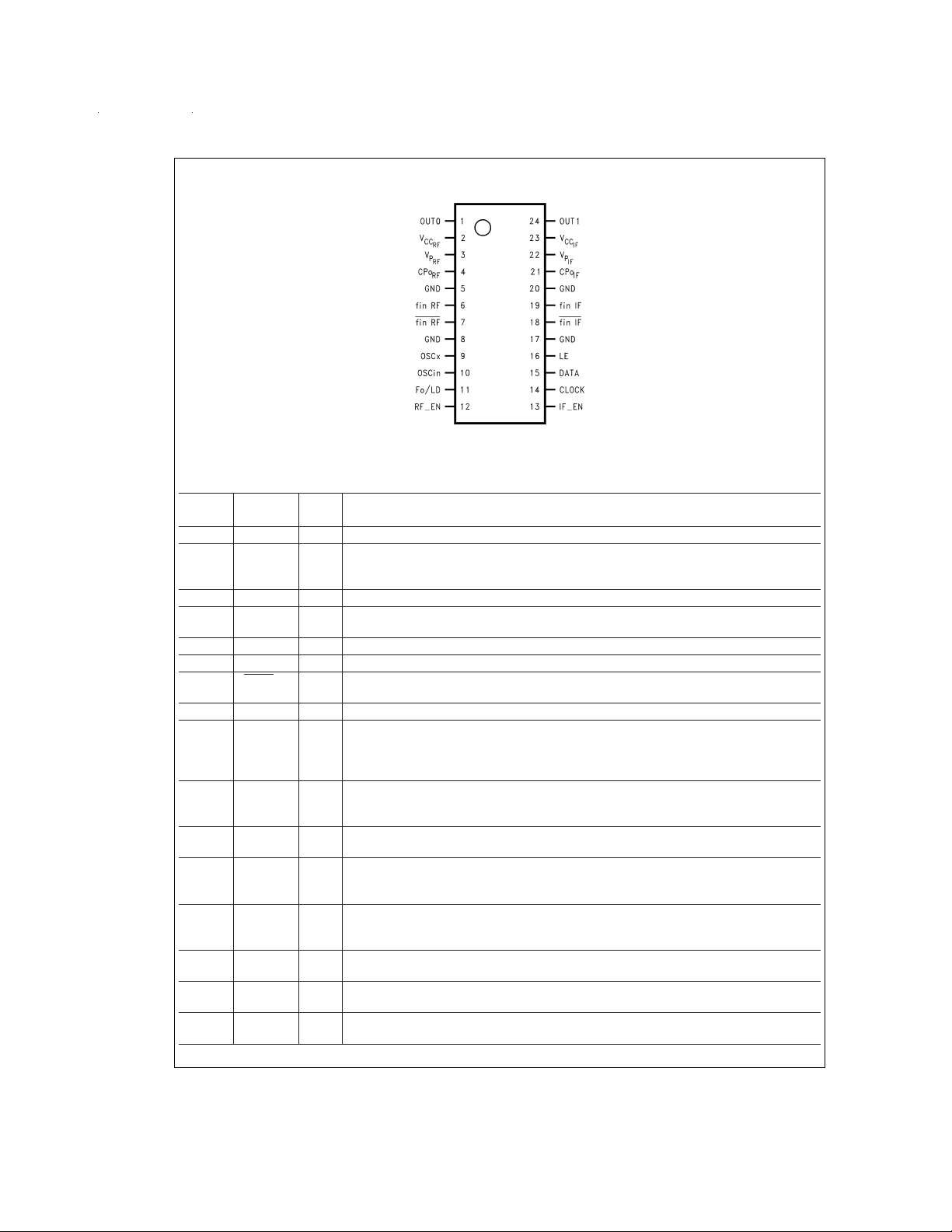
Connection Diagram
DS100831-2
Order Number LMX2350TM or LMX2352TM
NS Package Number MTC24
Pin Descriptions
Pin
No.
Pin
I/O Description
Name
1 OUT0 O Programmable CMOS output. Level of the output is controlled by IF_N [17] bit.
2 Vcc
RF
- RF PLL power supply voltage input. Must be equal to VccIF. May range from 2.7 V to 5.5 V.
Bypass capacitors should be placed as close as possible to this pin and be connected directly
to the ground plane.
3V
4CP
p
RF
o
RF
- Power supply for RF charge pump. Must be ≥V
O RF charge pump output. Connected to a loop filter for driving the control input of an external
VCO.
and V
cc
RF
.
cc
IF
5 GND - Ground for RF PLL digital circuitry.
6 fin RF I RF prescaler input. Small signal input from the VCO.
7 fin RF
I RF prescaler complimentary input. A bypass capacitor should be placed as close as possible
to this pin and be connected directly to the ground plane.
8 GND - Ground for RF PLL analog circuitry.
9 OSCx I/O Dual mode oscillator output or RF R counter input. Has a Vcc/2 input threshold when
configured as an input and can be driven from an external CMOS or TTL logic gate. Can also
be configured as an output to work in conjunction with OSCin to form a crystal oscillator. (See
functional description 1.1 and programming description 3.1.)
10 OSCin I Oscillator input which can be configured to drive both the IF and RF R counter inputs or only
the IF R counter depending on the state of the OSC programming bit. (See functional
description 1.1 and programming description 3.1.)
11 FoLD O Multiplexed output of N or R divider and RF/IF lock detect. Active High/Low CMOS output
except in analog lock detect mode. (See programming description 3.1.5.)
®
12 RF_EN I RF PLL Enable. Powers down RF N and R counters, prescaler, and will TRI-STATE
the
charge pump output when LOW. Bringing RF_EN high powers up RF PLL depending on the
state of RF_CTL_WORD. (See functional description 1.9.)
13 IF_EN I IF PLL Enable. Powers down IF N and R counters, prescaler, and will TRI-STATE the charge
pump output when LOW. Bringing IF_EN high powers up IF PLL depending on the state of
IF_CTL_WORD. (See functional description 1.9.)
14 CLOCK I High impedance CMOS Clock input. Data for the various counters is clocked into the 24 - bit
shift register on the rising edge.
15 DATA I Binary serial data input. Data entered MSB first. The last two bits are the control bits. High
impedance CMOS input.
16 LE I Load enable high impedance CMOS input. Data stored in the shift registers is loaded into one
of the 4 internal latches when LE goes HIGH. (See functional description 1.7.)
www.national.com 2
Connection Diagram (Continued)
Pin
No.
Pin
Name
I/O Description
17 GND - Ground for IF analog circuitry.
18 fin IF
I IF prescaler complimentary input. A bypass capacitor should be placed as close as possible
to this pin and be connected directly to the ground plane.
19 fin IF I IF prescaler input. Small signal input from the VCO.
20 GND - Ground for IF digital circuitry.
21 CPo
22 Vp
23 Vcc
IF
IF
IF
O IF charge pump output. For connection to a loop filter for driving the input of an external VCO.
- Power supply for IF charge pump. Must be ≥ V
and V
cc
RF
.
cc
IF
- IF power supply voltage input. Must be equal to VccRF. Input may range from 2.7 V to 5.5 V.
Bypass capacitors should be placed as close as possible to this pin and be connected directly
to the ground plane.
24 OUT1 O Programmable CMOS output. Level of the output is controlled by IF_N [18] bit.
www.national.com3
Absolute Maximum Ratings (Note 1)
If Military/Aerospace specified devices are required, please contact the National Semiconductor Sales Office/
Distributors for availability and specifications.
Value
Parameter Symbol Min Typ Max Units
Power Supply Voltage Vcc
Vcc
Vp
Vp
RF
IF
RF
IF
-0.3 6.5 V
-0.3 6.5 V
-0.3 6.5 V
-0.3 6.5 V
Voltage on any pin with GND = 0 volts Vi -0.3 Vcc + 0.3 V
Storage Temperature Range Ts -65 +150 C˚
Lead Temperature (Solder 4 sec.) T
L
+260 C˚
ESD - Whole Body Model (Note 2) 2 Kev
Recommended Operating Conditions
Value
Parameter Symbol Min Typ Max Units
Power Supply Voltage Vcc
Vcc
Vp
Vp
RF
IF
RF
IF
Operating Temperature TA -40 + 85 C
Note 1: “Absolute Maximum Ratings” indicate limits beyond which damage
to the device may occur. Operating Ratings indicate conditions for which the
device is intended to be functional, but do not guarantee specific performance limits.Forguaranteed specifications and test conditions, see the Electrical Characteristics. The guaranteed specifications apply only for the test
conditions listed.
=
Electrical Characteristics (V
Sym-
Parameter Conditions Min Typ Max Units
cc
=
V
cc
RF
IF
bol
General
I
cc
Power Supply Current LMX2350 RF and IF,
V
LMX2352 RF and IF,
V
LMX2350/52 IF only, V
I
CC-PWDN
f
in
Power Down Current RF_EN = IF_EN = LOW 5 µA
RF RF Operating LMX2350 Prescaler = 32 (Note 3) 1.2 2.5 GHz
Frequency Prescaler = 16 (Note 3) 0.5 1.2 GHz
LMX2352 Prescaler = 16 (Note 3) 0.5 1.2 GHz
Prescaler = 8 (Note 3) 0.25 0.5 GHz
f
IF IF Operating Frequency 10 550 MHz
in
f
OSC
Oscillator Frequency No load on OSCx (Note 3) 2 50 MHz
With resonator load on
OSCx (Note 3)
fφ Phase Detector Frequency RF and IF 10 MHz
Pf
in RF
RF Input Sensitivity VCC= 3.0V −15 0 dBm
V
Pf
in IF
V
OSC
IF Input Sensitivity 2.7 V≤VCC≤ 5.5V −10 0 dBm
Oscillator Sensitivity OSCin, OSCx 0.5 V
2.7 5.5 V
Vcc
RF
Vcc
RF
V
Vcc 5.5 V
Vcc 5.5 V
Note 2: ThisDevice is a high performance RF integrated circuit and is ESD
sensitive. Handling and assembly of this device should only be done at ESDfree workstations.
=
V
=
V
P
RF
3.0V; −40˚ C
P
IF
<
<
T
85˚ C except as specified)
A
6.75 7.75 mA
=
2.7V to 5.5V
cc
5.0 6.0 mA
=
2.7V to 5.5V
cc
=
2.7V to 5.5V 1.25 1.45 mA
cc
2 20 MHz
= 5.0V −10 0 dBm
CC
CC
V
PP
www.national.com 4
Electrical Characteristics (V
(Continued)
V
cc
RF
V
cc
IF
=
V
P
RF
3.0V; −40˚ C
P
IF
<
<
T
85˚ C except as specified)
A
=
=
=
Symbol Parameter Conditions Min Typ Max Units
Charge Pump
ICPo-
RF
ICPoICPo-
RF
ICPoICPo-
IF
ICPoICPo-
IF
ICPoICPo-
ICPovs.
ICPo-
ICPo vs.
VCPo
ICPo vs. T CP Current vs
RF Charge Pump
source
Output Current (see
Programming
sink RF
Description 3.2.2)
source
sink RF
IF Charge Pump Output
source
Current (see
Programming
sink IF
Description 3.1.4)
source
sink IF
Charge Pump
Tri
TRI-STATE Current
CP Sink vs. Source
sink
Mismatch
source
CP Current vs. Voltage 0.5 ≤ VCPo ≤ Vp -
Temperature
VCPo Vp/2, RF_CP_WORD = 0000 −100 µA
VCPo = Vp/2, RF_CP_WORD = 0000 100 µA
VCPo = Vp/2, RF_CP_WORD = 1111 −1.6 mA
VCPo = Vp/2, RF_CP_WORD = 1111 1.6 mA
VCPo = Vp/2, CP_GAIN_8 = 0 −100 µA
VCPo = Vp/2, CP_GAIN_8 = 0 100 µA
VCPo = Vp/2, CP_GAIN_8 = 1 −800 µA
VCPo = Vp/2, CP_GAIN_8 = 1 800 µA
0.5 ≤ VCPo ≤ Vp - 0.5
<TA<
-40˚ C
85˚ C
VCPo = Vp/2
TA = 25˚ C
0.5
= 25˚ C
T
A
VCPo = Vp/2
<TA<
-40˚ C
85˚ C
RFICPo
= 400 µA - 1.6 mA
RFICPo
= 800 µA - 1.6 mA
-2.5 2.5 nA
310
815
8
%
%
%
Digital Interface
V
IH
V
IL
I
IH
I
IL
I
IH
I
IL
V
OH
V
OL
High-level Input Voltage (Note 4) 0.8 Vcc V
Low-level Input Voltage (Note 4) 0.2 Vcc V
=
High-level Input Current V
Low-level Input Current V
Oscillator Input Current V
Oscillator Input Current V
High-level Output
Voltage
High-level Output
Voltage
I
I
=
V
IH
IL
IH
IL
OH
OL
5.5 V, (Note 4) −1.0 1.0 µA
CC
=
=
0, V
5.5 V, (Note 4) −1.0 1.0 µA
CC
=
=
V
5.5 V 100 µA
CC
=
=
0, V
5.5 V −100 µA
CC
=
−500 µA V
=
500 µA 0.4 V
−0.4 V
CC
MICROWIRE Timing
t
CS
t
CH
t
CWH
t
CWL
t
ES
t
EW
Note 3: Minimum operating frequencies are not production tested - only characterized.
Note 4: except fin, OSCin and OSCx
Data to Clock Setup
See Data Input Timing 50 ns
Time
Data to Clock Hold
See Data Input Timing 10 ns
Time
Clock Pulse Width High See Data Input Timing 50 ns
Clock Pulse Width Low See Data Input Timing 50 ns
Clock to Load Enable
See Data Input Timing 50 ns
Set Up Time
Load Enable Pulse
See Data Input Timing 50 ns
Width
www.national.com5
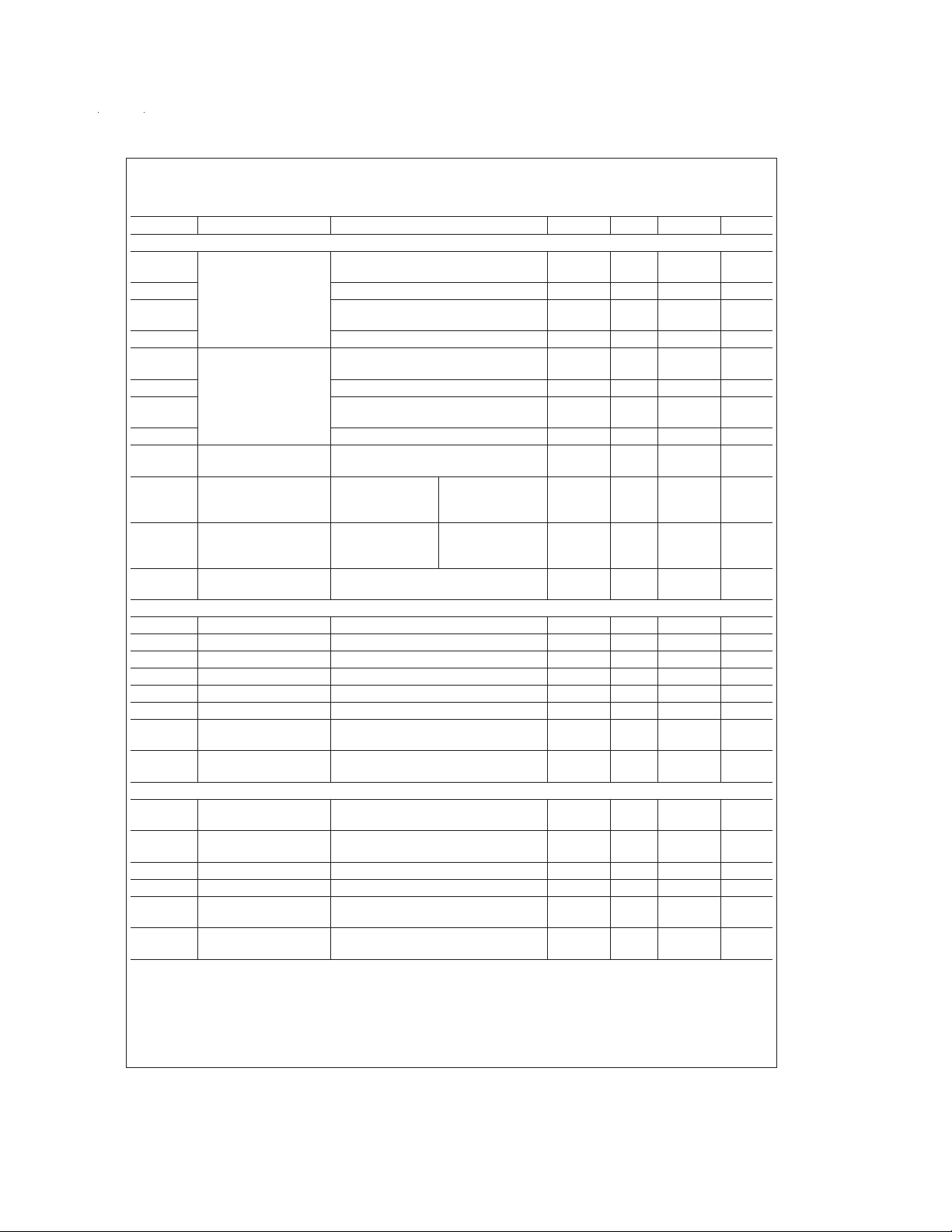
Charge Pump Current Specification Definitions
I1=CP sink current at V
I2=CP sink current at V
I3=CP sink current at V
I4=CP source current at V
I5=CP source current at V
I6=CP source current at V
∆V=Voltage offset from positive and negative rails. Dependent on VCO tuning range relative to V
Note 5: I
||6|}]
Note 6: I
Note 7: I
25˚C|]/||5@25˚C|*100
vs V
Do
*
%
100
Do-sink
vs T
Do
=
Vp − ∆V
Do
=
Vp/2
Do
=
∆V
Do
=
Vp − ∆V
Do
=
Vp/2
Do
=
∆V
Do
=
Charge Pump Output Current magnitude variation vs Voltage=[
Do
vs V
A
=
Charge Pump Output Current Sink vs Source Mismatch=[||2| − ||5|]/[
Do-source
=
Charge Pump Output Current magnitude variation vs Temperature=[||2
%
1
*
⁄
2
{||1| − ||3|}]/[1⁄
@
DS100831-7
and ground. Typical values are between 0.5V and 1.0V.
CC
*
2
{||1| + ||3|}]*100%and [1⁄
1
*
⁄
2
{||2| + ||5|}]*100
%
*
2
{||4| − ||6|}]/[1⁄
*
2
{||4| +
temp| − ||2@25˚C|]/||2@25˚C|*100%and [||5@temp| − ||5
@
www.national.com 6

RF Sensitivity Test Block Diagram
Note: N=10,000 R=50 P=64
Note: Sensitivity limit is reached when the error of the divided RF output, F
Typical Performance Characteristics
ICCvs V
CC
LMX2350
DS100831-9
I
TRI-STATE vs
CPO
CP
Voltage
O
LD, is ≥ 1 Hz.
o
ICCvs V
CC
LMX2352
Charge Pump Current vs CPOVoltage
RF_CP_WORD=0000 and 0111
IF CP_GAIN8=0 and 1
DS100831-8
DS100831-10
DS100831-11
DS100831-12
www.national.com7

Typical Performance Characteristics (Continued)
Charge Pump Current vs CP
RF_CP_WORD=0011 and 1111
RF Input Impedance
=
V
2.7V to 5.5V, f
CC
3 GHz (f
Capacitor=100 pF)
IN
=
IN
O
50 MHz to
Voltage
DS100831-13
Sink vs Source Mismatch
(See (Note 6) under Charge Pump Current
Specification Definitions)
IF Input Impedance
=
V
CC
1 GHz (f
2.7V to 5.5V, f
Capacitor=100 pF)
IN
=
IN
10 MHz to
DS100831-14
DS100831-15
www.national.com 8
DS100831-16

Typical Performance Characteristics (Continued)
LMX2350 RF Sensitivity vs Frequency
IF Input Sensitivity vs Frequency
DS100831-17
LMX2352 RF Sensitivity vs Frequency
DS100831-18
Oscillator Input Sensitivity vs Frequency
DS100831-19
LMX2350 VPVoltage vs VPLoad Current in Vdoubler
Mode, T=25˚C
DS100831-21
DS100831-20
www.national.com9

Functional Description
1.0 General
The basic phase-lock-loop (PLL) configuration consists of a
high-stability crystal reference oscillator, a frequency synthesizer such as the National Semiconductor LMX2350/52, a
voltage controlled oscillator (VCO), and a passive loop filter.
The frequency synthesizer includes a phase detector, current mode charge pump, as well as programmable reference
[R] and feedback [N] frequency dividers. The VCO frequency
is established by dividing the crystal reference signal down
via the R counter to obtain a frequency that sets the comparison frequency. This reference signal, fr, is then presented to
the input of a phase/frequency detector and compared with
another signal, fp, the feedback signal, which was obtained
by dividing the VCO frequency down by way of the N counter
and fractional circuitry. The phase/frequency detector’s current source outputs pump charge into the loop filter, which
then converts the charge into the VCO’s control voltage. The
phase/frequency comparator’s function is to adjust the voltage presented to the VCO until the feedback signal’s frequency (and phase) match that of the reference signal.
When this ’phase-locked’ condition exists, the RF VCO’s frequency will be N+F times that of the comparison frequency,
where N is the integer divide ratio and F is the fractional
component. The fractional synthesis allows the phase detector frequency to be increased while maintaining the same
frequency step size for channel selection. The division value
N is thereby reduced giving a lower phase noise referred to
the phase detector input, and the comparison frequency is
increased allowing faster switching times.
1.1 Reference Oscillator Inputs
The reference oscillator frequency for the RF and IF PLL’s is
provided by either an external reference through the OSCin
pin and OSCx pin, or an external crystal resonator across
the OSCin and OSCx pins. OSCin/OSCx block can operate
to 50MHz with an input sensitivity of 0.5Vpp. The OSC bit
(see programming description 3.1.1), selects whether the oscillator input pins OSCin and OSCx drive the IF and RF R
counters separately (Low) or by a common input signal path
(Hi). The common OSC mode allows the user to form a local
crystal oscillator circuit or drive the OSCin pin from an external signal source. When a crystal resonator is connected between OSCin and OSCx along with 2 external capacitors to
form a crystal oscillator both reference chains are driven simultaneously.When a TCXO is connected only at the OSCin
input pin and not at the OSCx pin, the TCXO drives both IF
R counter and RF R counter. When configured as separate
inputs, the OSCin pin drives the IF R counter while the OSCx
drives the RF R counter. The inputs have a Vcc/2 input
threshold and can be driven from an external CMOS or TTL
logic gate.
1.2 Reference Dividers (R Counters)
The RF and IF R Counters are clocked through the oscillator
block either separately or in common. The maximum frequency is 50MHz. Both R Counters are 15 bit CMOS
counters with a divide range from 3 to 32,767. (See programming description 3.1.3.)
1.3 Programmable Dividers (N Counters)
The RF and IF N Counters are clocked by the small signal fin
RF and fin IF input pins respectively. The LMX2350 RF N
counter is 19 bits with 15 bits integer divide and 4 bits fractional. The integer part is configured as a 5 bit ACounter and
a 10 bit B Counter. The LMX2350 is capable of operating
from 500 MHz to 1.2 GHz with the 16/17 prescaler offering a
continuous integer divide range from 272 to 16399, and 1.2
GHz to 2.5 GHz with the 32/33 prescaler offering a continuous integer divide range from 1056 to 32767. The LMX2352
RF N counter is 18 bits with 14 bits integer divide and 4 bits
fractional. The integer part is configured as a 4 bit A Counter
and a 10 bit B Counter. The LMX2352 is capable of operating from 250 MHz to 500 MHz with the 8/9 prescaler offering
a continuous integer divide range from 72 to 8199, and
500MHz to 1.2 GHz with 16/17 prescaler offering a continuous integer divide range from 272 to 16383. The RF
counters for the LMX2350 family also contain fractional compensation, programmable in either 1/15 or 1/16 modes. Both
LMX2350 and LMX2352 IF N counters are 15 bit integer dividers configured with a 3 bit A Counter and a 12 bit B
Counter offering a continuous integer divide range from 56 to
32,767 over the frequency range of 10 MHz to 550 MHz. The
IF N counters do not include fractional compensation.
1.3.1 Prescaler
The RF and IF inputs to the prescaler consist of fin and /fin;
which are complimentary inputs to differential pair amplifiers.
The complimentary inputs are internally coupled to ground
with a 10 pF capacitor. These inputs are typically AC coupled
to ground through external capacitors as well. The input
buffer drives the A counter’s ECL D-type flip flops in a dual
modulus configuration. A 16/17 or 32/33 prescale ratio can
be selected for the LMX2350, and the lower frequency
LMX2352 provides 8/9 or 16/17 prescale ratios. The IF circuitry for both the LMX2350 and LMX2352 contain an 8/9
prescaler. The prescaler clocks the subsequent CMOS flipflop chain comprising the fully programmable A and B
counters.
1.3.2 Fractional Compensation
The fractional compensation circuitry of the LMX2350 and
LMX2352 RF dividers allow the user to adjust the VCO’s tuning resolution in 1/16 or 1/15 increments of the phase detector comparison frequency. A 4 bit register is programmed
with the fractions desired numerator, while another bit selects between fractional 15 and 16 modulo base denominator (see programming description 4.2.4). An integer average
is accomplished by using a 4 bit accumulator. A variable
phase delay stage compensates for the accumulated integer
phase error, minimizing the charge pump duty cycle, and reducing spurious levels. This technique eliminates the need
for compensation current injection in to the loop filter. Overflow signals generated by the accumulator are equivalent to
1 full VCO cycle, and result in a pulse swallow.
1.4 Phase/Frequency Detector
The RF and IF phase(/frequency) detectors are driven from
their respective N and R counter outputs. The maximum frequency at the phase detector inputs is about 2 MHz for some
high frequency VCO due to the minimum continuous divide
ratio of the dual modulus prescaler (i.e. If the VCO output frequency is 2.4816 GHz, the maximum phase detector input
frequency is 2.35 MHz because the minimum continuous divide ratio of the LMX2350 with 32/33 prescaler is 1056). The
phase detector outputs control the charge pumps. The polarity of the pump-up or pump-down control is programmed using RF_PD_POL or IF_PD_POL depending on whether
RF/IF VCO characteristics are positive or negative (see programming descriptions 3.1.4 and 3.2.2). The phase detector
also receives a feedback signal from the charge pump, in order to eliminate dead zone.
www.national.com 10

Functional Description (Continued)
1.5 Charge Pump
The phase detector’s current source outputs pump charge
into an external loop filter, which then converts the charge
into the VCO’s control voltage. The charge pumps steer the
charge pump output, CPo, to Vcc (pump-up) or ground
(pump-down). When locked, CPo is primarily in a
TRI-STATE
pump output current magnitude is programmable from 100
µA to 1.6 mA in 100 µA steps as shown in table in programming description 3.2.2. The IF charge pump is set to either
100µAor 800µA levels using bit IF_R [19] (see programming
description 3.1.4).
1.6 Voltage Doubler
The Vp
ply over a range of Vcc to 5.5v to provide current for the RF
charge pump circuit. An internal voltage doubler circuit connected between the Vcc and VpRF supply pins alternately
allows Vcc = 3v (
circuit at close to twice the Vcc power supply voltage. The
voltage doubler mode is enabled by setting the V2_EN bit
(RF_R [22]) to a HIGH level. The voltage doubler’s charge
pump driver originates from the RF oscillator input (OSCx).
The device will not totally powerdown until the V2_EN bit is
programmed low. The average delivery current of the doubler is less than the instantaneous current demand of the RF
charge pump when active and is thus not capable of sustaining a continuous out of lock condition. A large external capacitor connected to Vp
power supply droop when changing frequencies. Refer to
the application note AN-1119 for more details.
1.7 MICROWIRE
The programmable functions are accessed through the MICROWIRE serial interface. The interface is made of 3 functions: clock, data and latch enable (LE). Serial data for the
various counters is clocked in from data on the rising edge of
clock, into the 24- bit shift register.Data is entered MSB first.
The last two bits decode the internal register address. On the
rising edge of LE, data stored in the shift register is loaded
into one of the 4 appropriate latches (selected by address
bits). A complete programming description is included in the
following sections.
1.8 Fo/LD Multifunction Output
The Fo/LD output pin can deliver several internal functions
including analog/digital lock detects, and counter outputs.
See programming description 3.1.5 for more details.
1.8.1 Lock Detect
A digital filtered lock detect function is included with each
phase detector through an internal digital filter to produce a
logic level output available on the Fo/LD output pin if selected. The lock detect output is high when the error between
the phase detector inputs is less than 15 nsec for 5 consecutive comparison cycles. The lock detect output is low when
the error between the phase detector outputs is more than
30 nsec for one comparison cycle. An analog lock detect signal is also selectable. The lock detect output is always low
when the PLL is in power down mode. See programming descriptions 3.1.5, 4.6 - 4.8 for more details.
®
mode with small corrections. The RF charge
pin is normally driven from an external power sup-
RF
±
10%) users to run the RF charge pump
is therefore needed to control
RF
™
Serial Interface
1.9 Power Control
Each PLL is individually power controlled by device enable
pins or MICROWIRE power down bits. The enable pins override the power down bits except for the V2_EN bit. The
RF_EN pin controls the RF PLL; IF_EN pin controls the IF
PLL. When both pins are high, the power down bits determine the state of power control (see programming description 3.2.1.2). Activation of any PLL power down mode results
in the disabling of the respective N counter and de-biasing of
its respective Fin input (to a high impedance state). The R
counter functionality also becomes disabled when the power
down bit is activated. The reference oscillator block powers
down and the OSCin pin reverts to a high impedance state
when both RF and IF enable pins or power down bit’s are asserted, unless the V2_EN bit (RF_R[22]) is high. Power
down forces the respective charge pump and phase comparator logic to a TRI-STATE condition. A power down
counter reset function resets both N and R counters. Upon
powering up the N counter resumes counting in “close” alignment with the R counter (The maximum error is one prescaler cycle). The MICROWIRE control register remains active and capable of loading and latching in data during all of
the power down modes.
www.national.com11

Programming Description
2.0 INPUT DATA REGISTER
The descriptions below describe the 24-bit data register loaded through the MICROWIRE Interface. The data register is used to
program the 15-bit IF_R counter register, and the 15-bit RF_R counter register, the 15-bit IF_N counter register, and the 19-bit
RF_N counter register. The data format of the 24-bit data register is shown below. The control bits CTL [1:0] decode the internal
register address. On the rising edge of LE, data stored in the shift register is loaded into one of the 4 appropriate latches (selected
by address bits). Data is shifted in MSB first
MSB LSB
DATA [21:0] CTL [1:0]
23 2 1 0
2.1 Register Location Truth Table
CTL [1:0] DATA Location
10
0 0 IF_R register
0 1 IF_N register
1 0 RF_R register
1 1 RF_N register
2.2 Register Content Truth Table
First Bit REGISTER BIT LOCATION Last Bit
23 22 212019 18 17 1615141312111098765 4 3 2 10
IF_R OSC FRAC_16 FoLD IF_CP_WORD IF_R_CNTR 0 0
IF_N IF_CTL_WORD CMOS IF_NB_CNTR IF_NA_CNTR 0 1
RF_R DLL_MODE V2_EN RF_CP_WORD RF_R_CNTR 1 0
RF_N RF_CTL_WORD RF_NB_CNTR RF_NA_CNTR FRAC_CNTR 1 1
3.0 PROGRAMMABLE REFERENCE DIVIDERS
3.1 IF_R Register
If the Control Bits (CTL [1:0]) are 0 0, when LE is transitioned high data is transferred from the 24-bit shift register into a latch
which sets the IF PLL 15-bit R counter divide ratio. The divide ratio is programmed using the bits IF_R_CNTR as shown in table
3.1.3. The ratio must be ≥ 3. The IF_CP_WORD [1:0], programs the IF charge pump magnitude and polarity shown in 3.1.4. The
OSC bit is used to enable the crystal oscillator mode. FoLD [2:0] is used to set the function of the Lock Detect output (pin 11),
according to table 3.1.3.
MSB LSB
OSC FRAC_16 FoLD [2:0] IF_CP_WORD [1:0] IF_R_CNTR [14:0] 0 0
23 22 21 19 18 17 16 2 1 0
3.1.1 OSC (IF_R[23])
The OSC bit, IF_R [23], selects whether the oscillator input pins OSCin and OSCx drive the IF and RF R counters separately or
by a common input signal path. When the OSC bit = 1, a crystal resonator can be connected between OSCin and OSCx together
with 2 capacitors to form a crystal oscillator. When OSC=0,theOSCin pin drives the IF R counter while the OSCx drives the
RF R counter.
3.1.2 FRAC_16 (IF_R[22])
The FRAC_16 bit, IF_R [22], is used to set the fractional compensation at either 1/16 and 1/15 resolution. When FRAC-16 is set
to one, the fractional modulus is set to 1/16 resolution, and FRAC_16 = 0 corresponds to 1/15 (See section 4.2.4).
www.national.com 12

Programming Description (Continued)
3.1.3 15-BIT PROGRAMMABLE REFERENCE DIVIDER RATIO (R COUNTER) (IF_R[2]-[16])
IF_R_CNTR/RF_R_CNTR
Divide Ratio 14 13 12 11 109876543210
3 000000000000011
4 000000000000100
- ---------------
32,767 111111111111111
Notes: Divide ratio: 3 to 32,767 (Divide ratios less than 3 are prohibited).
RF_R_CNTR/IF_R_CNTR These bits select the divide ratio of the programmable reference dividers.
3.1.4 IF_CP_WORD (IF_R[17]-[18])
IF_CP_WORD (IF_R [17] - [18] )
CP_GAIN_8 IF_PD_POL
BIT LOCATION FUNCTION 0 1
CP_GAIN_8 IF_R [18] IF Charge Pump Current Gain 1X 8X
IF_PD_POL IF_R [17] IF Phase Detector Polarity Negative Positive
CP_GAIN_8 is used to toggle the IF charge pump current magnitude between 1x mode (100 uA typ) and 8x mode (800uA typ).
IF_PD_POL is set to one when IF VCO characteristics are positive. When IF VCO frequency decreases with increasing control
voltage IF_PD_POL should set to zero.
3.1.5 FoLD* Programming Truth Table (IF_R[19]-[21])
FoLD Fo/LD OUTPUT STATE
0 0 0 IF and RF Analog Lock Detect (Open Drain)
1 0 0 IF Digital Lock Detect
0 1 0 RF Digital Lock Detect
1 1 0 IF and RF Digital Lock Detect
0 0 1 IF R counter
1 0 1 IF N counter
0 1 1 RF R counter
1 1 1 RF N counter
*FoLD - Fout/Lock Detect PROGRAMMING BITS
3.2 RF_R Register
If the Control Bits (CTL [1:0]) are 1 0, data is transferred from the 24-bit shift register into the RF_R register latch which sets the
RF PLL 15-bit R counter divide ratio. The divide ratio is programmed using the RF_R_CNTR word as shown in table 3.1.3. The
divide ratio must be ≥ 3. The bits used to control the voltage doubler (V2_EN) and RF Charge Pump (RF_CP_WORD) are detailed in 3.2.2.
MSB LSB
DLL_MODE V2_EN RF_CP_WORD [4:0] RF_R_CNTR [14:0] 1 0
23 22 21 17 16 2 1 0
www.national.com13

Programming Description (Continued)
3.2.1 (RF_R [22 - 23] )
DLL_MODE V2_EN
BIT LOCATION FUNCTION 0 1
DLL_MODE RF_R [23] Delay Line Loop Calibration
Mode
V2_EN RF_R [22] RF_Voltage Doubler Enable Disabled Enabled
1. V2_EN bit when set high enables the voltage doubler for the RF Charge Pump supply.
2. DLL_MODE bit should be set to one for normal usage.
3.2.2 RF_CP_WORD (RF_R[17]-[21])
CP_8X CP_4X CP_2X CP_1X RF_PD_POL
RF_PD_POL ( RF_R[17] ) should be set to one when RF VCO characteristics are positive. When RF VCO frequency decreases
with increasing control voltage RF_PD_POL should be set to zero.
CP_1x, CP_2x, CP_4x, and CP_8x are used to step the RF Charge Pump output current magnitude from 100 uA to 1.6 mA in
100uA steps as shown in the table below.
RF Charge Pump Output Truth Table
ICPo uA (typ) CP8x CP4x CP2x CP1x
RF_R[21] RF_R[20] RF_R[19] RF_R[18]
100 0000
200 0001
300 0010
400 0011
- ----
900 1000
- ----
1600 1111
4.0 PROGRAMMABLE DIVIDERS (N COUNTERS)
4.1 IF_N Register
If the Control Bits (CTL [1:0]) are 01, data is transferred from the 24-bit shift register into the IF_N register latch which sets the
PLL 15 bit programmable N counter value and various control functions. The IF_N counter consists of the 3-bit swallow counter
(A counter), and the 12 bit programmable counter (B counter). Serial data format is shown below in tables 4.1.2 and 4.1.3. The
divide ratio (IF_NB_CNTR) must be ≥3. The divide ratio is programmed using the bits IF_N_CNTR as shown in tables 4.1.2 and
4.1.3. The divide ratio must be ≥56. The CMOS [3:0] bits program the 2 CMOS outputs detailed in section 4.4.
MSB LSB
IF_CTL_WORD [2:0] CMOS [3:0] IF_NB_CNTR [11:0] IF_NA_CNTR [2:0] 0 1
23 21 20 17 16 5 4 2 1 0
4.1.1 IF_CTL_WORD (IF_R[21]-[23])
MSB LSB
IF_CNT_RST PWDN_IF PWDN_MODE
Note: See section 4.2.1.2 for IF control word truth table.
Slow Fast
www.national.com 14

Programming Description (Continued)
4.1.2 3-BIT IF SWALLOW COUNTER DIVIDE RATIO (IF A COUNTER) (IF_N[2]−[4])
Swallow Count IF_NA_CNTR
(A) 2 1 0
0 000
1 001
- ---
Note: Swallow Counter Value: 0 to 7
IF_NB_CNTR ≥ IF_NA_CNTR
Minimum continuous count = 56 ( A=0, B=7)
4.1.3 12-BIT IF PROGRAMMABLE COUNTER DIVIDE RATIO (IF B COUNTER) (IF_N[5]-[16])
Divide Ratio 11 109876543210
3 0 0 0000000011
4 0 0 0000000100
- - - ----------
4,095 1 1 1111111111
Note: Divide ratio: 3 to 4095 (Divide ratios less than 3 are prohibited)
IF_NB_CNTR ≥ IF_NA_CNTR
N divider continuous integer divide ratio 56 to 32,767.
4.2 RF_N Register
If the control bits (CTL[2:0]) are 11, data is transferred from the 24-bit shift register into the RF_N register latch which sets the RF
PLL 19 bit programmable N counter register and various control functions. The RF N counter consists of the 5-bit swallow counter
(A counter) the 10 bit programmable counter (B counter), and 4 bit fractional counter. Serial data format is shown below. The divide ratio (RF_NB_CNTR) must be ≥3, and must be ≥ the swallow counter value + 2; RF_NB_CNTR≥ ( RF_NA_CNTR+2).
MSB LSB
RF_CTL_WORD [2:0] RF_NB_CNTR [9:0] RF_NA_CNTR [4:0] FRAC_CONT [3:0] 1 1
23 21 20 11 10 6 5 2 1 0
4.2.1.1 RF_CTL_WORD (RF_N[21]-[23])
4.2.1.2 RF/IF Control Word Truth Table
IF_CNT_RST/RF_CNT_RST IF/RF counter reset Normal Operation Reset
PWDN_IF/PWDN_RF IF/RF power down Powered up Powered down
PWDN_MODE Power down mode select Asynchronous power down Synchronous power down
PRESC LMX2350 Prescaler Modulus select 16/17
The Counter Reset enable bit when activated allows the reset of both N and R counters. Upon powering up, the N
counter resumes counting in ″close″ alignment with the R
counter (the maximum error is one prescaler cycle).
Activation of the PLL power down bits result in the disabling
of the respective N counter divider and de-biasing of its respective fin inputs (to a high impedance state). The respective R counter functionality also becomes disabled when the
power down bit is activated. The OSCin pin reverts to a high
impedance state when both RF and IF power down bits are
asserted. Power down forces the respective charge pump
7 111
IF_NB_CNTR
MSB LSB
RF_CNT_RST PWDN_RF PRESC_SEL
BIT FUNCTION 0 1
32/33
(0.5 to 1.2 GHz operation)
LMX2352 8/9
(0.25 to 0.5 GHz operation)
(1.2 to 2.5 GHz operation)
16/17
(0.5 to 1.2 GHz operation)
and phase comparator logic to a TRI-STATE condition. The
MICROWIRE control register remains active and capable of
loading and latching in data during all of the power down
modes.
Both synchronous and asynchronous power down modes
are available with the LMX2350 family in order to adapt to
different types of applications. The power down mode bit
IF_N[21] is used to select between synchronous and asynchronous power down. The MICROWIRE control register remains active and capable of loading and latching in data during all of the power down modes.
www.national.com15

Programming Description (Continued)
Synchronous Power down Mode
One of the PLL loops can be synchronously powered down
by first setting the power down mode bit HIGH (IF_N[21] = 1)
and then asserting its power down bit (IF_N[22] or RF_N[22]
= 1). The power down function is gated by the charge pump.
Once the power down bit is loaded, the part will go into
power down mode upon the completion of a charge pump
pulse event.
Asynchronous Power down Mode
One of the PLL loops can be asynchronously powered down
by first setting the power down mode bit LOW (IF_N[21] = 0)
and then asserting its power down bit (IF_N[22] or RF_N[22]
= 1). The power down function is NOT gated by the charge
pump. Once the power down bit is loaded, the part will go
into power down mode immediately.
Prescaler select is used to set the RF prescaler. The
LMX2350 is capable of operating from 500 MHz to 1.2 GHz
with the 16/17 prescaler, and 1.2 GHz to 2.5 GHz with the
32/33 prescaler selection. The LMX2352 is capable of operating from 250 MHz to 500 MHz with the 8/9 prescaler, and
500MHz to 1.2GHz with 16/17 prescaler selection.
4.2.2 5-BIT RF SWALLOW COUNTER DIVIDE RATIO
(RF A COUNTER) (RF_N[6]-[10])
Swallow Count RF_NA_CNTR
(A) 43210
0 00000
1 00001
- -----
31 11111
Note: Swallow Counter Value LMX2350: 0 to 31; LMX2352: 0 to 15
RF_NB_CNTR ≥ RF_NA_CNTR + 2
4.2.3 10-BIT RF PROGRAMMABLE COUNTER DIVIDE
RATIO (RF B COUNTER) (RF_N[11]-[20])
RF_NB_CNTR
Divide Ratio 9876543210
3 0000000011
4 0000000100
- ----------
1,023 1111111111
Note: Divide ratio: 3 to 1023 (Divide ratios less than 3 are prohibited)
RF_NB_CNTR ≥ RF_NA_CNTR + 2
4.2.4 FRACTIONAL MODULUS ACCUMULATOR (FRAC_CNTR) (RF_N[2]-[5])
Fractional Ratio (F) FRAC_CNTR
Modulus 15 Modulus 16 RF_N[5] RF_N[4] RF_N[3] RF_N[2]
0 0 0000
1/15 1/16 0001
2/15 2/16 0010
- - ----
14/15 14/16 1110
N/A 15/16 1111
4.3 PULSE SWALLOW FUNCTION
fvco = [N + F] x [fosc/R]
N=(PxB)+A
F: Fractional ratio (contents of FRAC_CNTR divided by
the fractional modulus)
fvco: Output frequency of external voltage controlled oscil-
lator (VCO)
B: Preset divide ratio of binary 10-bit programmable
counter
A: Preset value of binary 4 or 5-bit swallow counter (0 ≤
fosc: Output frequency of the external reference frequency
oscillator
R: Preset divide ratio of binary 15-bit programmable ref-
erence counter (3 to 16383)
P: Preset modulus of dual modulus prescaler
(LMX2350:RF P=16 or 32, IF P=8)
(LMX2352:RF P=8 or 16, IF P=8)
A≤ 31 {RF} , 0 ≤ A ≤ 15 {IF} , A+2 ≤ B {RF}, A ≤ B {IF})
4.4 CMOS (Programmable CMOS outputs) (IF_N[17]-[20])
MSB LSB
FastLock TEST OUT_1 OUT_0
Note: Test bit is reserved and should be set to zero for normal usage.
www.national.com 16

Programming Description (Continued)
4.4.1 Programmable CMOS Output Truth Table
BIT LOCATION FUNCTION 0 1
OUT_0 IF_N[17] OUT0 CMOS output pin level
set
OUT_1 IF_N[18] OUT1 CMOS output pin level
set
FastLock IF_N[20] FastLock mode select CMOS output FastLock mode
When the FastLock bit is set to one, OUT_0 and OUT_1 are don’t care bits. FastLock mode utilizes the OUT0 and OUT1 output
pins to synchronously switch between active low and TRI-STATE.The OUT0 = LOW state occurs whenever the RF loop’s CP_8X
is selected HIGH while the FastLock bit is set HIGH (see programming description 3.2.2). The OUT0 pin reverts to TRI-STATE
when the CP_8X bit is LOW.Similarly for the IF loop, the synchronous activation of OUT1= LOW or TRI-STATE, is dependent on
whether the CP_GAIN_8 is high or low respectively (see programming description 3.1.4).
4.5 SERIAL DATA INPUT TIMING
Note: Data shifted into register on clock rising edge. Data is shifted in MSB first.
TEST CONDITIONS: The Serial Data Input Timing is tested using a symmetrical waveform around Vcc/2. The test waveform has an edge rate of 0.6 V/nsec
with amplitudes of 2.2V
@
Vcc=2.7 V and 2.6V@Vcc = 5.5 V.
LOW HIGH
LOW HIGH
DS100831-3
www.national.com17

Programming Description (Continued)
4.6 LOCK DETECT DIGITAL FILTER
The Lock Detect Digital Filter compares the difference between the phase of the inputs of the phase detector to a RC generated
delay of approximately 15nS. To enter the locked state (Lock = HIGH) the phase error must be less than the 15nS RC delay for
5 consecutive reference cycles. Once in lock (Lock = HIGH), the RC delay is changed to approximately 30nS. To exit the locked
state (Lock = LOW), the phase error must become greater than the 30nS RC delay. When the PLL is in the power down mode,
Lock is forced LOW. A flow chart of the digital filter is shown at right.
www.national.com 18
DS100831-4

Programming Description (Continued)
4.7 ANALOG LOCK DETECT FILTER
When the Fo/LD output is configured in analog lock detect mode an external lock detect circuit is needed in order to provide a
steady LOW signal when the PLL is in the locked state. Atypical circuit is shown below. The fold output is active low (open drain)
only when analog lock detect mode is selected.
DS100831-5
4.8 TYPICAL LOCK DETECT TIMING
DS100831-6
www.national.com19

Physical Dimensions inches (millimeters) unless otherwise noted
Synthesizer
Molded TSSOP, JEDEC Plastic Package (MTC24)
Order Number LMX2350TM or LMX2352TM
NS Package MTC24
LIFE SUPPORT POLICY
NATIONAL’S PRODUCTS ARE NOT AUTHORIZED FOR USE AS CRITICAL COMPONENTS IN LIFE SUPPORT
DEVICES OR SYSTEMS WITHOUT THE EXPRESS WRITTEN APPROVAL OF THE PRESIDENT AND GENERAL
COUNSEL OF NATIONAL SEMICONDUCTOR CORPORATION. As used herein:
1. Life support devices or systems are devices or
systems which, (a) are intended for surgical implant
into the body, or (b) support or sustain life, and
whose failure to perform when properly used in
accordance with instructions for use provided in the
2. A critical component is any component of a life
support device or system whose failure to perform
can be reasonably expected to cause the failure of
the life support device or system, or to affect its
safety or effectiveness.
labeling, can be reasonably expected to result in a
significant injury to the user.
National Semiconductor
Corporation
LMX2350/LMX2352 PLLatinumTM Fractional N RF / Integer N IF Dual Low Power Frequency
Americas
Tel: 1-800-272-9959
Fax: 1-800-737-7018
Email: support@nsc.com
www.national.com
National does not assume any responsibility for use of any circuitry described, no circuit patent licenses are implied and National reserves the right at any time without notice to change said circuitry and specifications.
National Semiconductor
Europe
Fax: +49 (0) 1 80-530 85 86
Email: europe.support@nsc.com
Deutsch Tel: +49 (0) 1 80-530 85 85
English Tel: +49 (0) 1 80-532 78 32
Français Tel: +49 (0) 1 80-532 93 58
Italiano Tel: +49(0) 1 80-534 16 80
National Semiconductor
Asia Pacific Customer
Response Group
Tel: 65-2544466
Fax: 65-2504466
Email: sea.support@nsc.com
National Semiconductor
Japan Ltd.
Tel: 81-3-5639-7560
Fax: 81-3-5639-7507
 Loading...