

查询LMX2323供应商
LMX2323
LMX2323 PLLatinum 2.0 GHz Frequency Synthesizer for RF Personal Communications
October 2000
PLLatinum
™
2.0 GHz Frequency Synthesizer for RF
Personal Communications
General Description
The LMX2323 is a high performance frequency synthesizer
with integrated 32/33 dual modulus prescaler designed for
RF operation up to 2.0 GHz. Using a proprietary digital
phase locked loop technique, the LMX2323’s linear phase
detector characteristics can generate very stable, low noise
control signals for UHF and VHF voltage controlled oscillators.
Serial data is transferred into the LMX2323 via a three-line
MICROWIRE
range is from 2.7V to 5.5V. The LMX2323 features very low
curent consumption, typically 3.5mAat3V.Thecharge pump
provides 4 mA output current.
The LMX2323 is manufactured using National’s ABiC V
BiCMOS process and is packaged in a 16-pin TSSOP.
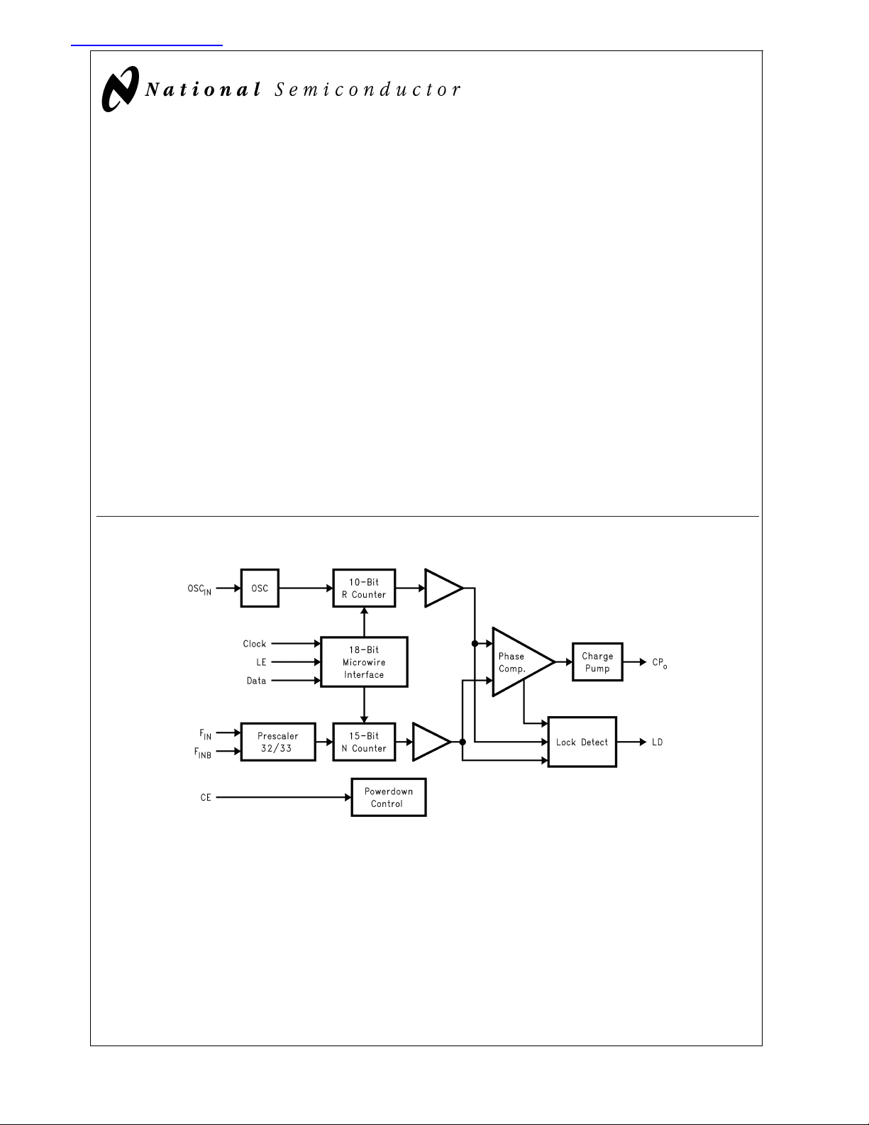
Functional Block Diagram
™
interface (Data, LE, Clock). Supply voltage
Features
n RF operation up to 2.0 GHz
n 2.7V to 5.5V operation
n Low current consumption: Icc = 3.5mA (typ) at
Vcc=3.0V
n Digital Lock Detect
n Dual modulus prescaler: 32/33
n Internal balanced, low leakage charge pump
Applications
n Cellular telephone systems (GSM, NADC, CDMA, PDC,
PHS)
n Personal wireless communications (DCS-1800, DECT,
CT-1+)
n Wireless local area networks (WLANs)
n DCS/PCS infrastructure equipment
n Other wireless communication systems
DS101362-1
TRI-STATE®is a registered trademark of National Semiconductor Corporation.
MICROWIRE
© 2000 National Semiconductor Corporation DS101362 www.national.com
™
and PLLatinum™are trademarks of National Semiconductor Corporation.
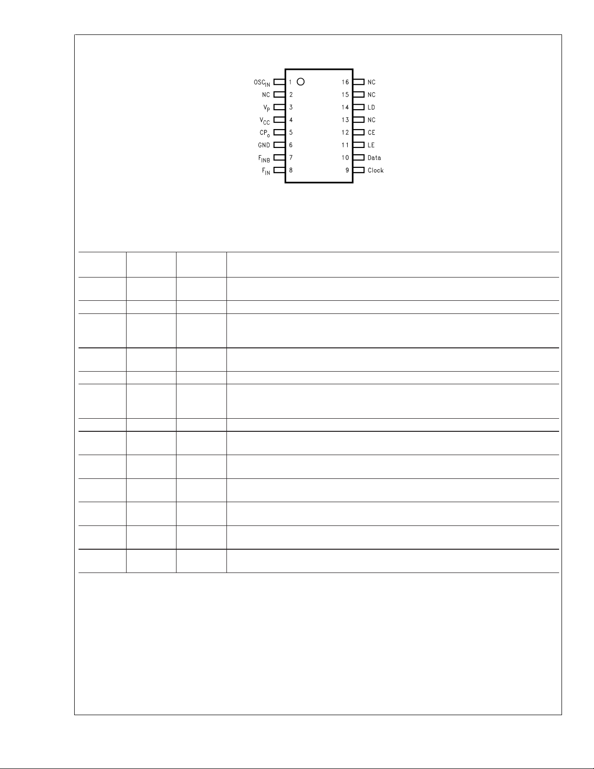
Connection Diagram
LMX2323
Pin Descriptions
DS101362-2
Top View
Order Number LMX2323TM, LMX2323TMX
See NS Package Number MTC16
Pin No.
1 OSC
Pin
Name
I/O Description
IN
I Oscillator input. A CMOS inverting gate input. The input has a VCC/2 input threshold
and can be driven from an external CMOS or TTL logic gate.
3V
4V
P
CC
— Power supply for charge pump. Must be ≥ VCC.
— Power supply voltage input. Input may range from 2.7V to 5.5V. Bypass capacitors
should be placed as close as possible to this pin and be connected directly to the
ground plane.
5CP
o
O Internal charge pump output. For connection to a loop filter for driving the voltage
control input of an external oscillator.
6 GND — Ground.
7f
INB
I RF prescaler complimentary input. In single-ended mode, a bypass capacitor should
be placed as close as possible to this pin and be connected directly to the ground
plane. The LMX2323 can be driven differentially when a bypass capacitor is omitted.
8f
IN
I RF prescaler input. Small signal input from the voltage controlled oscillator.
9 Clock I High impedance CMOS Clock input. Data is clocked in on the rising edge, into the
various counters and registers.
10 Data I Binary serial data input. Data entered MSB first. LSB is control bit. High impedance
CMOS input.
11 LE I Load Enable input. When Load Enable transitions HIGH, data is loaded into either the
N or R register (control bit dependent). See timing diagram.
12 CE I PLL Enable. A LOW on CE powers down the device asynchronously and
TRI-STATE
®
s the charge pump output.
14 LD O Lock detect output. This pin can be programmed to provide R counter output, N
counter output, digital lock detect (CMOS logic) or analog lock detect (open drain).
2, 13,
NC No Connect.
15, 16
www.national.com 2
LMX2323
Absolute Maximum Ratings (Note 1)
Power Supply Voltage (V
Power Supply for Charge Pump (V
Voltage on Any Pin with
GND=0V(V
) −0.3V to VCC+ 0.5V
I
Storage Temperature Range (T
Lead Temperature (solder, 4 sec.) (T
ESD - Whole Body Model (Note 2) 2 kV
) −0.3V to 6.5V
CC
)V
P
) −65˚C to +150˚C
S
) +260˚C
L
CC
to 6.5V
Recommended Operating
Conditions
Power Supply Voltage (V
Power Supply for Charge pump (V
Operating Temperature (T
Note 1: Absolute Maximum Ratings indicate limits beyond which damage to
the device may occur. Operating Conditions indicate conditions for which the
device is intended to be functional. For guaranteed specifications and test
conditions, see the Electrical Characteristics.
Note 2: This device is a high performance RF integrated circuit and is ESD
sensitive. Handling and assembly of this device should be done on ESD
protected workstations.
(Note 1)
CC
) 2.7V to 5.5V
)V
P
) −40˚C to +85˚C
A
CC
to 5.5V
Electrical Characteristics
VCC= 3.0V, VP= 3.0V; −40˚C<T
Symbol Parameter Conditions Min Typ Max Units
GENERAL
I
CC
I
CC
I
-PWDN VCC= 5.5V (Note 3) 10 20 µA
CC
f
IN
f
OSC
Power Supply Current VCC= 3.0V 3.5 mA
RF Operating Frequency 0.1 2.0 GHz
Oscillator Frequency 5 40 MHz
fφ Phase Detector Frequency 10 MHz
Pf
IN
V
OSC
RF Input Sensitivity 2.7V≤Vcc≤ 3.0V -15 0 dBm
Oscillator Sensitivity 0.4 0.8 VCC-0.3 V
Phase Noise (Note 4) fIN= 900 MHz, V
CHARGE PUMP
I
CPo-source
I
CPo-sink
I
CPo-Tri
Charge Pump Output Current V
Charge Pump TRI-STATE
Current
I
vs
CPo
V
CPo
I
CPo-sink
I
CPo-source
I
vs T Charge Pump Output Current
CPo
Charge Pump Output Current
Magnitude Variation vs Voltage
vs
Charge Pump Output Current
Sink vs Source Mismatch
Magnitude Variation vs
Temperature
DIGITAL INTERFACE (DATA, CLK,LE, CE)
V
OH
V
OL
V
IH
High-Level Output Voltage IOH= −500 µA VCC−0.4 V
Low-Level Output Voltage IOL= −500 µA 0.4 V
High-Level Input Voltage
(Note 5)
V
IL
I
IH
Low-Level Input Voltage (Note 5) 0.2Vcc V
High-Level Input Current (Clock,
Data, Load Enable)
I
IL
Low-Level Input Current (Clock,
Data, Load Enable)
I
IH
I
IL
Oscillator Input Current VIH=VCC= 5.5V 100 µA
Oscillator Input Current VIL=0,VCC= 5.5V −100 µA
<
85˚C except as specified.
A
VCC= 2.7V to 5.5V 7.0 mA
<
3.0
f
= 900 MHz, V
IN
f
= 1800 MHz, V
IN
f
= 1800 MHz, V
IN
CPo=VP
V
CPo=VP
0.5 ≤ V
0.5 ≤ V
= 25˚C
T
A
V
CPo=VP
= 25˚C
T
A
V
CPo=VP
VIH=VCC= 5.5V
VIL=0,VCC= 5.5V
Vcc≤5.0V -10 0 dBm
PP
OSC
OSC
OSC
OSC
≥ 0.8 V
≥ 0.4 V
≥ 0.8 V
≥ 0.4 V
PP
PP
PP
PP
−86
−82
−82
−80
(Note 6) dBc/Hz
/2 −4.3 mA
/2 4.3 mA
≤ VP- 0.5
CPo
CPo
/2
≤ VP- 0.5
−2.5 2.5 nA
10 %
5%
/2
8%
0.8Vcc V
−1.0 1.0 µA
−1.0 1.0 µA
www.national.com3
Electrical Characteristics (Continued)
VCC= 3.0V, VP= 3.0V; −40˚C<T
LMX2323
Symbol Parameter Conditions Min Typ Max Units
MICROWIRE TIMING
t
CS
t
CH
t
CWH
t
CWL
t
ES
t
EW
Note 3: This ICC-PWDN represents CLK, DATA, LE and CE being tied to either higher than 0.8 VCCor lower than 0.2 VCC.
Note 4: Phase noise is measured 1 kHz off from the carrier frequency. Comparison frequency is 200 kHz. OSC
Note 5: Except f
Note 6: Typical values are determined from measurements on the reference evaluation boards. A 3 dB (3 sigma) degradation is estimated from statistical distribution
in manufacturing. Units will NOT be tested in production.
Data to Clock Set Up Time See Data Input Timing 50 ns
Data to Clock Hold Time See Data Input Timing 10 ns
Clock Pulse Width High See Data Input Timing 50 ns
Clock Pulse Width Low See Data Input Timing 50 ns
Clock to Enable Set Up Time See Data Input Timing 50 ns
Enable Pulse Width See Data Input Timing 50 ns
and OSCIN.
IN
<
85˚C except as specified.
A
frequency is 13 MHz.
IN
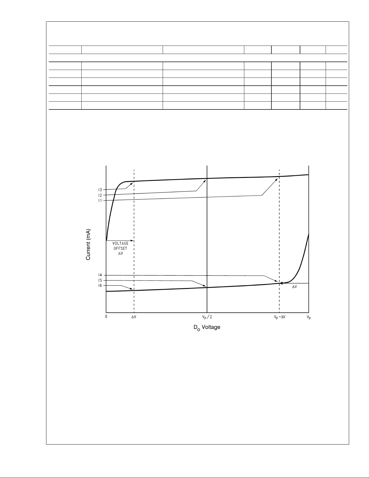
Charge Pump Current Specification Definitions
I1 = CP sink current at VCPo=VP−∆V
I2 = CP sink current at VCP
I3 = CP sink current at VCP
I4 = CP source current at VCP
I5 = CP source current at VCP
I6 = CP source current at VCP
∆V = Voltage offset from positive and negative rails. Dependent on VCO tuning range relative to V
vs VCPo= Charge Pump Output Current magnitude variation vs Voltage =
1. ICP
o
1
*
⁄
2
{|I1| − |I3|}] / [1⁄
[
2. ICP
3. ICP
vs ICP
o-sink
[|I2| − |I5|] / [
vs TA= Charge Pump Output Current magnitude variation vs Temperature =
o
@
temp| − |I2@25˚C|] / |I2@25˚C|*100% and [|I5@temp| − |I5@25˚C|] / |I5@25˚C|*100%
[|I2
*
2
o-source
1
*
⁄
2
{|I2| + |I5|}]*100%
/2
o=VP
= ∆V
o
−∆V
o=VP
/2
o=VP
= ∆V
o
{|I1| + |I3|}]*100% and [1⁄
= Charge Pump Output Current Sink vs Source Mismatch =
*
2
{|I4| − |I6|}] / [1⁄
*
2
{|I4| + |I6|}]*100%
www.national.com 4
DS101362-4
and ground. Typical values are between 0.5V and 1.0V.
CC

Typical Performance Characteristics
LMX2323
ICCvs V
CC
DS101362-13
RF Input Sensitivity vs Frequency
Charge Pump Current vs VCPo Output
DS101362-14
Oscillator Input Sensitivity
DS101362-15
DS101362-16
www.national.com5

1.0 Functional Description
The basic phase-lock-loop (PLL) configuration consists of a
LMX2323
high-stability crystal reference oscillator, a frequency synthesizer such as the National Semiconductor LMX2323, a voltage controlled oscillator (VCO), and a passive loop filter. The
frequency synthesizer includes a phase detector, current
mode charge pump, as well as programmable reference [R]
and feedback [N] frequency dividers. The VCO frequency is
established by dividing the crystal reference signal down via
the R counter to obtain a frequency that sets the comparison
frequency. This reference signal, f
input of a phase/frequency detector and compared with another signal, f
, the feedback signal, which was obtained by
p
dividing the VCO frequency down by way of the N counter.
The phase/frequency detector’s current source outputs
pump charge into the loop filter, which then converts the
charge into the VCO’s control voltage. The phase/frequency
comparator’s function is to adjust the voltage presented to
the VCO until the feedback signal’s frequency (and phase)
match that of the reference signal. When this “phase-locked”
condition exists, the RF VCO’s frequency will be N times that
of the comparison frequency, where N is the divider ratio.
1.1 OSCILLATOR
The reference oscillator frequency for the PLL is provided by
an external reference TCXO through the OSC
block can operate to 40 MHz. The inputs have a VCC/2 input
threshold and can be driven from an external CMOS or TTL
logic gate.
1.2 REFERENCE DIVIDER (R COUNTER)
The R Counter is clocked through the oscillator block. The
maximum input frequency is 40 MHz and the maximum
output frequency is 10 MHz. The R Counter is a 10-bit
CMOS binary counter with a divide range from 2 to 1,023.
See programming description 2.2.1.
1.3 PROGRAMMABLE DIVIDER (N COUNTER)
The N counter is clocked by the small signal f
LMX2323 RF N counter is a 15-bit integer divider. The N
counter is configured as a 5-bit A Counter and a 10-bit B
Counter, offering a continuous integer divide range from 992
to 32,767. The LMX2323 is capable of operating from
100 MHz to 2.0 GHz with a 32/33 prescaler.
1.3.1 Prescaler
The RF inputs to the prescaler consist of the f
which are the complimentary inputs of a differential pair
amplifier. The differential f
2 GHz. The input buffer drives the N counter’s ECL D-type
flip-flops in a dual modulus configuration. The LMX2323 has
a 32/33 prescaler ratio. The prescaler clocks the subsequent
CMOS flip-flop chain comprising the fully programmable A
and B counters.
1.4 PHASE/FREQUENCY DETECTOR
The phase/frequency detector is driven from the N and R
counter outputs. The maximum frequency at the phase detector inputs is 10 MHz. The phase detector outputs control
the charge pumps. The polarity of the pump-up or pumpdown control is programmed using PD_POL, depending on
whether RF VCO characteristics are positive or negative
(see programming description 2.2.2). The phase detector
also receives a feedback signal from the charge pump, in
order to eliminate dead zone.
, is then presented to the
r
IN
configuration can operate to
IN
pin. OSC
IN
input. The
IN
and f
INB
pins
1.5 CHARGE PUMP
The phase detector’s current source output pumps charge
into an external loop filter, which then converts the charge
into the VCO’s control voltage. The charge pumps steer the
charge pump output, CP
(pump-down). When locked, CP
,toVP(pump-up) or Ground
o
is primarily in a TRI-STATE
o
mode with small corrections. The RF charge pump output
current magnitude is set to 4.0 mA. The charge pump output
can also be used to output divider signals as detailed in
section 2.2.3.
1.6 MICROWIRE SERIAL INTERFACE
The programmable functions are accessed through the
MICROWIRE serial interface. The interface is made of three
functions: clock, data and latch enable (LE). Serial data for
the various counters is clocked in from data on the rising
edge of clock, into the 18-bit shift register. Data is entered
MSB first. The last bit decodes the internal register address.
On the rising edge of LE, data stored in the shift register is
loaded into one of the two appropriate latches (selected by
address bits). A complete programming description is included in the following sections.
1.7 LOCK DETECT OUTPUT
A digital filtered lock detect function is included through an
IN
internal digital filter to produce a CMOS logic output available on the LD output pin if selected. The lock detect output
is high when the error between the phase detector inputs is
less than 15 ns for five consecutive comparison cycles. The
lock detect output is low when the error between the phase
detector input is more than 30 ns for one comparison cycle.
An open drain, analog lock detect status generated from the
phase detector is also available on the LD output pin, if
selected. The analog lock detect output goes high when the
charge pump is inactive. It goes low when the charge pump
is active during a comparison cycle. When the PLL is in
power down mode, the LD output is always high.
1.8 POWER CONTROL
The PLL can be power controlled in two ways. The first
method is by setting the CE pin LOW. This asynchronously
powers down the PLL and TRI-STATEs the charge pump
output, regardless of the PWDN bit status. The second
method is by programming through MICROWIRE, while
keeping the CE HIGH. Programming the PWDN bit in the N
register HIGH (CE = HIGH) will disable the N counter and
de-bias the f
input (to a high impedance state). The R
IN
counter functionality also becomes disabled. The reference
oscillator block powers down when the power down bit is
asserted. The OSC
pin reverts to a high impedance state
IN
when this condition exists. Power down forces the charge
pump and phase comparator logic to a TRI-STATEcondition.
A power down counter reset function resets both N and R
counters. Upon powering up the N counter resumes counting in “close” alignment with the R counter (the maximum
error is one prescaler cycle). The MICROWIRE control register remains active and capable of loading and latching in
data during all of the power down modes.
www.national.com 6

2.0 Programming Description
2.1 MICROWIRE INTERFACE
The MICROWIRE interface is comprised of an 18-bit shift register, a R register and a N register. The shift register consists of a
17-bit DATAfield and a 1-bit address (ADDR) field as shown below. When Latch Enable transitions HIGH, data stored in the shift
register is loaded into either the R or N register depending on the ADDR bit as described in Table2.1.1. The data is loaded MSB
first. The DATA field assignment for the R and N registers are shown in Table 2.1.2 below.
MSB LSB
DATA [16:0] ADDR
17 1 0
2.1.1 Address Bit Truth Table
When LE is transitioned high, data is transferred from the 18-bit shift register into either the 14-bit R register, or the 17-bit N
register depending upon the state of the ADDR bit.
ADDR DATA Location
0 N register
1 R register
2.1.2 Register Content Truth Table
MSB SHIFT REGISTER BIT LOCATION LSB
1716151413 12 11 109876543 2 1 0
N Register NB_CNTR NA_CNTR CTL_WORD 0
R Register X X LD_OUT PD_POL CP_TRI R_CNTR 1
LMX2323
2.2 R REGISTER
If the Address Bit (ADDR) is 1, when LE is transitioned high data is transferred from the 18-bit shift register into the 14-bit R
register. The R register contains a latch which sets the PLL 10-bit R counter divide ratio. The divide ratio is programmed using
the bits R_CNTR as shown in
PD_POL and CP_TRI bits control the phase detector polarity and charge pump TRI-STATE respectively, as shown in
R[12] Truth Table
First Bit SHIFT REGISTER BIT LOCATION Last Bit
1716151413 12 11 109876543210
X X LD_OUT PD_POL CP_TRI R_CNTR [9:0] 1
. X denotes a don’t care condition.
2.2.1 10-Bit Programmable Reference Divider Ratio (R Counter)
. The ratio must be ≥ 2. The
2.2.2 R[11],
2.2.1 10-Bit Programmable Reference Divider Ratio (R Counter)
R_CNTR
Divide Ratio 9876543210
2 0000000010
3 0000000011
• ••••••••••
1,023 1111111111
Note: Divide ratio: 2 to 1,023 (Divide ratios less than 2 are prohibited).
R_CNTR—These bits select the divide ratio of the programmable reference dividers.
2.2.2 R[11], R[12] Truth Table
Bit Location Function 0 1
CP_TRI R[11] Charge Pump TRI-STATE Normal Operation TRI-STATE
PD_POL R[12] Phase Detector Polarity Negative Positive
Note: Depending upon VCO characteristics, R[12] shoud be set accordingly. When VCO characteristics are positive, R[12] should be set HIGH. When VCO
characteristics are negative, R[12] should be set LOW.
www.national.com7

2.0 Programming Description (Continued)
2.2.3 LD_OUT Truth Table (R[13]-[15])
LMX2323
LD Pin Output R[15] R[14] R[13]
Digital Lock Detect 0 0 0
Analog Lock Detect 0 0 1
R Divider Output 0 1 0
N Divider Output 0 1 1
Test Mode 1 0 0
Note: Do not use Test mode in normal operation. Test mode is for factory testing purpose only. It allows direct testing of the digital lock detect by using the CLK and
Data as the R and N counter outputs.
The Lock Detect Digital Filter compares the phase difference of the inputs from the phase detector to a RC generated delay of
approximately 15 ns. To enter the locked state (LD = High), the phase error must be less than the 15 ns RC delay for 5
consecutive reference cycles. Once in lock, the RC delay is changed to approximately 30 ns. To exit the locked state, the phase
error must be greater than the 30 ns RC delay. When the PLL is in power down mode, LD is forced to High state. A flow chart of
the digital filter is shown as below:
www.national.com 8

2.0 Programming Description (Continued)
LMX2323
DS101362-5
2.3 N REGISTER
If the address bit is LOW (ADDR = 0), when LE is transitioned high, data is transferred from the 18-bit shift register into the 17-bit
N register. The N register consists of the 5-bit swallow counter (A counter), the 10-bit programmable counter (B counter) and the
control word. Serial data format is shown below in
Programmable Counter Divide Ratio (B Counter)
section
2.3.3 Pulse Swallow Function
First Bit SHIFT REGISTER BIT LOCATION Last Bit
17161514131211109876543 2 1 0
NB_CNTR [9:0] NA_CNTR [4:0] CTL_WORD [1:0] 0
.
2.3.1 5-Bit Swallow Counter Divide Ratio (A Counter)
and
2.3.2 10-Bit
. The pulse swallow function which determines the divide ratio is described in
www.national.com9

2.0 Programming Description (Continued)
2.3.1 5-Bit Swallow Counter Divide Ratio (A Counter)
LMX2323
Swallow Count NA_CNTR
(A) 43210
0 00000
1 00001
• •••••
31 11111
Notes: Swallow Counter Value: 0 to 31
NB_CNTR ≥ NA_CNTR
2.3.2 10-Bit Programmable Counter Divide Ratio (B Counter)
NB_CNTR
Divide Ratio 9876543210
3 0000000011
4 0000000100
• ••••••••••
1023 1111111111
Notes: Divide ratio: 3 to 1,023 (Divide ratios less than 3 are prohibited).
NB_CNTR ≥ NA_CNTR
2.3.3 Pulse Swallow Function
The N divider counts such that it divides the VCO RF frequency by (P+1) A times, and then divides by P (B - A) times. The B value
(NB_CNTR) must be ≥ 3. The continuous divider ratio is from 992 to 32,767. Divider ratios less than 992 are achievable as long
as the binary counter value is greater than the swallow counter value (NB_CNTR ≥ NA_CNTR).
f
=Nx(f
VCO
N=(PxB)+A
f
: Output frequency of external voltage controlled oscillator (VCO)
VCO
f
: Output frequency of the external reference frequency oscillator
OSC
R: Preset divide ratio of binary 10-bit programmable reference counter (2 to 1023)
N: Preset divide ratio of main 15-bit programmable integer N counter (992 to 32,767)
B: Preset divide ratio of binary 10-bit programmable B counter (3 to 1023)
A: Preset value of binary 5-bit swallow A counter (0 ≤ A ≤ 31, A ≤ B)
P: Preset modulus of dual modulus prescaler (P = 32)
OSC
/R)
2.3.4 CTL_WORD
MSB LSB
N2 N1
CNT_RST PWDN
2.3.4.1 Reserve Word Truth Table
CE CNT_RST PWDN Function
1 0 0 Normal Operation
1 0 1 Synchronous Powerdown
1 1 0 Counter Reset
1 1 1 Asynchronous Powerdown
0 X X Asynchronous Powerdown
Notes: X denotes don’t care.
1. The Counter Reset bit when activated allows the reset of both N and R counters. Upon powering up the N counter resumes
counting in “close” alignment with the R counter. (The maximum error is one prescaler cycle).
www.national.com 10

2.0 Programming Description (Continued)
2. Both synchronous and asynchronous power down modes are available with the LMX2323 to be able to adapt to different
types of applications. The MICROWIRE control register remains active and capable of loading and latching in data during all
of the powerdown modes.
Synchronous Power down Mode
The PLL loops can be synchronously powered down by setting the counter reset mode bit to LOW (N[2] = 0) and its power down
mode bit to HIGH (N[1] = 1). The power down function is gated by the charge pump. Once the power down mode and counter
reset mode bits are loaded, the part will go into power down mode upon the completion of a charge pump pulse event.
Asynchronous Power down Mode
The PLL loops can be asynchronously powered down by setting the counter reset mode bit to HIGH (N[2] = 1) and its power down
mode bit to HIGH (N[1] = 1). The power down function is NOT gated by the charge pump. Once the power down and counter reset
mode bits are loaded, the part will go into power down mode immediately.
The R and N counters are disabled and held at load point during the synchronous and asynchronous power down modes. This
will allow a smooth acquisition of the RF signal when the PLL is programmed to power up. Upon powering up, both R and N
counters will start at the ‘zero’ state, and the relationship between R and N will not be random.
Serial Data Input Timing
LMX2323
Notes: Parenthesis data indicates programmable reference divider data.
Data shifted into register on clock rising edge.
Data is shifted in MSB first.
Test Conditions: The Serial Data Input Timing is tested using a symmetrical waveform around V
amplitudes of 2.2V
@
VCC= 2.7V and 2.6V@VCC= 5.5V.
/2. The test waveform has an edge rate of 0.6 V/ns with
CC
Phase Comparator and Internal Charge Pump Characteristics
Notes: Phase difference detection range: −2π to +2π
The minimum width pump up and pump down current pulses occur at the CP
: Phase comparator input from the R divider
f
r
: Phase comparator input from the N divider
f
p
: Charge pump output
CP
o
pin when the loop is locked. PD_POL = 1
o
DS101362-6
DS101362-7
www.national.com11

Physical Dimensions inches (millimeters) unless otherwise noted
16-Pin Thin Shrink Small Outline Package
Order Number LMX2323TM, LMX2323TMX
NS Package Number MTC16
LIFE SUPPORT POLICY
NATIONAL’S PRODUCTS ARE NOT AUTHORIZED FOR USE AS CRITICAL COMPONENTS IN LIFE SUPPORT
DEVICES OR SYSTEMS WITHOUT THE EXPRESS WRITTEN APPROVAL OF THE PRESIDENT AND GENERAL
COUNSEL OF NATIONAL SEMICONDUCTOR CORPORATION. As used herein:
1. Life support devices or systems are devices or
systems which, (a) are intended for surgical implant
into the body, or (b) support or sustain life, and
whose failure to perform when properly used in
accordance with instructions for use provided in the
2. A critical component is any component of a life
support device or system whose failure to perform
can be reasonably expected to cause the failure of
the life support device or system, or to affect its
safety or effectiveness.
labeling, can be reasonably expected to result in a
LMX2323 PLLatinum 2.0 GHz Frequency Synthesizer for RF Personal Communications
significant injury to the user.
National Semiconductor
Corporation
Americas
Tel: 1-800-272-9959
Fax: 1-800-737-7018
Email: support@nsc.com
www.national.com
National does not assume any responsibility for use of any circuitry described, no circuit patent licenses are implied and National reserves the right at any time without notice to change said circuitry and specifications.
National Semiconductor
Europe
Fax: +49 (0) 180-530 85 86
Email: europe.support@nsc.com
Deutsch Tel: +49 (0) 69 9508 6208
English Tel: +44 (0) 870 24 0 2171
Français Tel: +33 (0) 1 41 91 8790
National Semiconductor
Asia Pacific Customer
Response Group
Tel: 65-2544466
Fax: 65-2504466
Email: ap.support@nsc.com
National Semiconductor
Japan Ltd.
Tel: 81-3-5639-7560
Fax: 81-3-5639-7507
 Loading...