

查询LMX2305供应商
LMX2305 PLLatinum 550 MHz Frequency Synthesizer
for RF Personal Communications
LMX2305
PLLatinum
TM
550 MHz Frequency Synthesizer
for RF Personal Communications
General Description
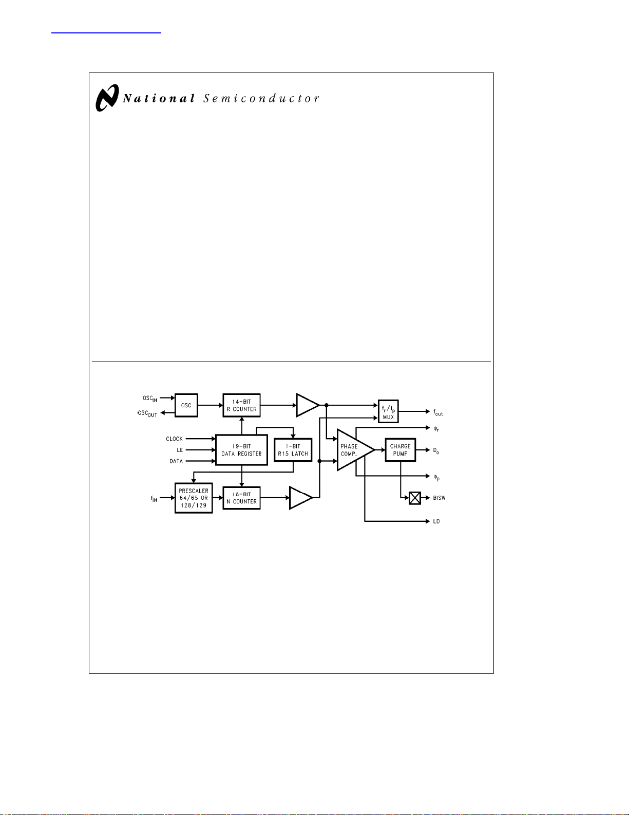
The LMX2305 is a high performance frequency synthesizer
with an integrated prescaler designed for RF operation up to
550 MHz. It is fabricated using National’s ABiC IV BiCMOS
process.
The LMX2305 contains a dual modulus prescaler which can
select either a 64/65 or a 128/129 divide ratio at input frequencies of up to 550 MHz. LMX2305, which employs the
digital phase lock loop technique, combined with a high
quality reference oscillator and a loop filter, provides the
tuning voltage for the voltage controlled oscillator to generate a very stable, low noise local oscillator signal.
Serial data is transferred into the LMX2305 via a three line
MICROWIRE
age can range from 2.65V to 5.5V. The LMX2305 features
very low current consumption, typically 4.0 mA at 2.75V.
The LMX2305 is available in a TSSOP 20-pin surface mount
plastic package.
TM
interface (Data, Enable, Clock). Supply volt-
Block Diagram
Features
Y
RF operation up to 550 MHz
Y
2.65V to 5.5V operation
Y
Low current consumption:
I
CC
Y
Dual modulus prescaler: 64/65 or 128/129
Y
Internal balanced, low leakage charge pump
Y
Small-outline, plastic, surface mount TSSOP,
0.173
Applications
Y
Analog Cellular telephone systems
(AMPS, ETACS, NMT)
Y
Portable wireless communications
(PCS/PCN, cordless)
Y
Wireless local area networks (WLANs)
Y
Other wireless communication systems
Y
Pagers
e
4.0 mA (typ) at V
wide package
×
PRELIMINARY
e
2.75V
CC
August 1996
TRI-STATEÉis a registered trademark of National Semiconductor Corporation.
TM
MICROWIRE
C
1996 National Semiconductor Corporation RRD-B30M126/Printed in U. S. A.
and PLLatinumTMare trademarks of National Semiconductor Corporation.
TL/W/12459
TL/W/12459– 1
http://www.national.com
Connection Diagram
LMX2305
20-Lead (0.173×Wide) Thin Shrink
TL/W/12459– 2
Small Outline Package (TM)
Order Number LMX2305TM or LMX2305TMX
See NS Package Number MTC20
Pin Descriptions
Pin No. Pin Name I/O Description
1 OSC
3 OSC
4V
5V
6D
IN
OUT
P
CC
o
7 GND Ground.
8 LD O Lock detect. Output provided to indicate when the VCO frequency is in ‘‘lock’’. When the loop is
10 f
IN
11 CLOCK I High impedance CMOS Clock input. Data is clocked in on the rising edge, into the various
13 DATA I Binary serial data input. Data entered MSB first. LSB is control bit. High impedance CMOS input.
14 LE I Load enable input (with internal pull-up resistor). When LE transitions HIGH, data stored in the
15 FC I Phase control select (with internal pull-up resistor). When FC is LOW, the polarity of the phase
16 BISW O Analog switch output. When LE is HIGH, the analog switch is ON, routing the internal charge
17 f
18 w
OUT
p
19 PWDN I Power Down (with internal pull-up resistor).
20 w
r
2,9,12 NC No connect.
I Oscillator input. A CMOS inverting gate input intended for connection to a crystal resonator for
operation as an oscillator. The input has a V
external CMOS or TTL logic gate. May also be from a reference oscillator.
/2 input threshold and can be driven from an
CC
O Oscillator output.
Power supply for charge pump. Must betVCC.
Power supply voltage input. Input may range from 2.65V to 5.5V. Bypass capacitors should be
placed as close as possible to this pin and be connected directly to the ground plane.
O Internal charge pump output. For connection to a loop filter for driving the input of an external
VCO.
locked, the pin’s output is HIGH with narrow low pulses.
I Prescaler input. Small signal input from the VCO.
counters and registers.
shift registers is loaded into the appropriate latch (control bit dependent). Clock must be low
when LE toggles high or low. See Serial Data Input Timing Diagram.
comparator and charge pump combination is reversed.
pump output through BISW (as well as through D
).
o
O Monitor pin of phase comparator input. CMOS output.
O Output for external charge pump. wpis an open drain N-channel transistor and requires a pull-up
resistor.
e
PWDN
PWDNeLOW for power saving.
Power down function is gated by the return of the charge pump to a TRI-STATE condition.
HIGH for normal operation.
O Output for external charge pump. wris a CMOS logic output.
http://www.national.com 2
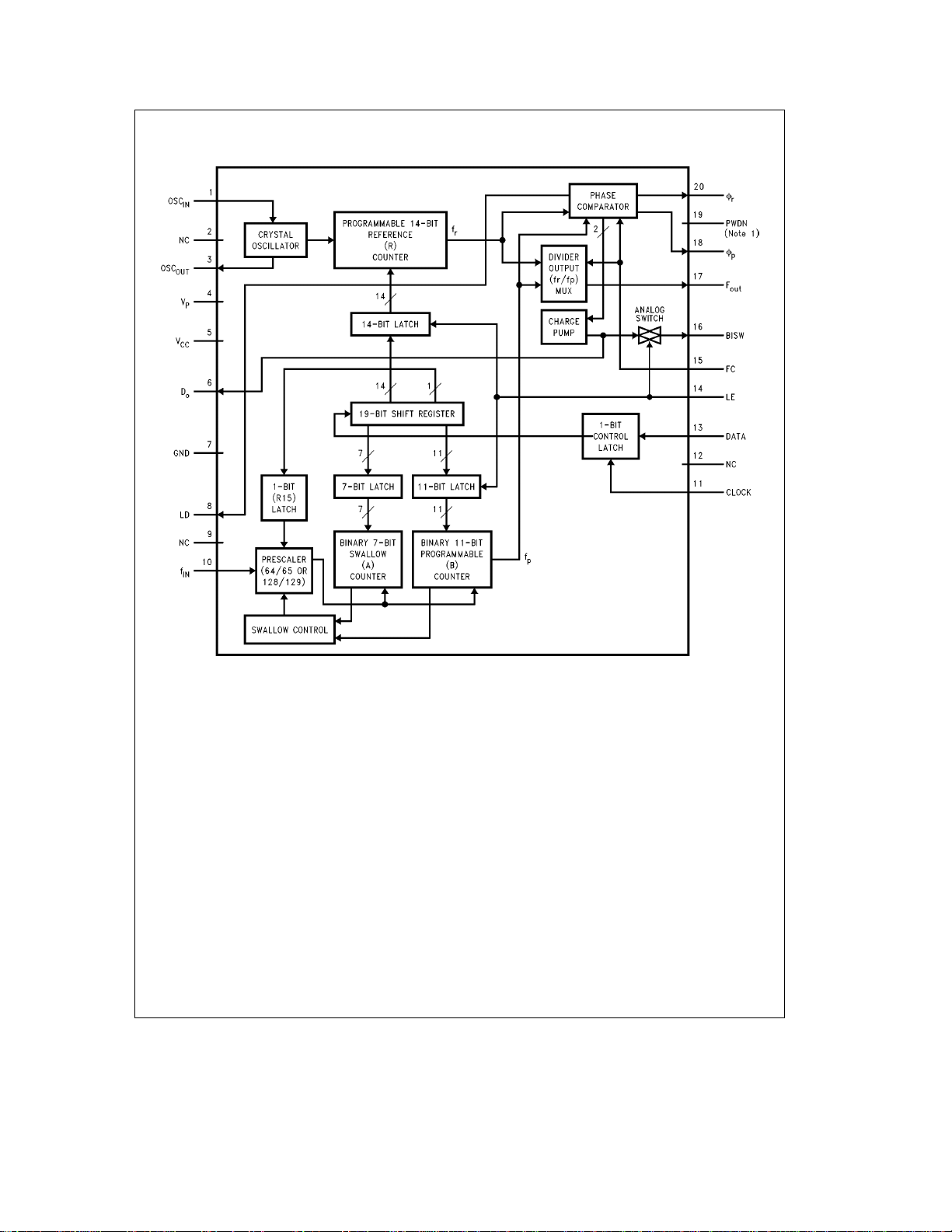
Functional Block Diagram
Note 1: The power down function is gated by the charge pump to prevent any unwanted frequency jumps. Once the power down pin is brought low the part will go
into power down mode when the charge pump reaches a TRI-STATE condition.
TL/W/12459– 3
http://www.national.com3
Absolute Maximum Ratings (Notes 1 and 2)
If Military/Aerospace specified devices are required,
please contact the National Semiconductor Sales
Office/Distributors for availability and specifications.
Power Supply Voltage
V
CC
V
P
Voltage on Any Pin
with GND
e
0V (VI)
Storage Temperature Range (TS)
Lead Temperature (TL) (solder, 4 sec.)
b
0.3V toa6.5V
b
0.3V toa6.5V
b
0.3V to V
b
65§Ctoa150§C
CC
a
a
0.3V
260§C
Recommended Operating
Conditions
Power Supply Voltage
V
CC
V
P
Operating Temperature (TA)
Note 1: Absolute Maximum Ratings indicate limits beyond which damage to
the device may occur. Operating Ratings indicate conditions for which the
device is intended to be functional, but do not guarantee specific performance limits. For guaranteed specifications and test conditions, see the Electrical Characteristics. The guaranteed specifications apply only for the test
conditions listed.
Note 2: This device is a high performance RF integrated circuit with an ESD
k
2 keV and is ESD sensitive. Handling and assembly of this device
rating
should only be done at ESD workstations.
2.65V to 5.5V
VCCtoa5.5V
b
40§Ctoa85§C
Electrical Characteristics V
CC
e
2.75V, V
e
2.75V;b40§CkT
P
k
85§C, except as specified
A
Symbol Parameter Conditions Min Typ Max Units
I
CC
I
CC-PWDN
f
IN
f
OSC
f
w
Pf
IN
V
OSC
V
IH
V
IL
I
IH
I
IL
I
IH
I
IL
I
IH
I
IL
*Except fINand OSC
Power Supply Current 4 6 mA
Power Down Current 30 180 mA
RF Input Operating Frequency 45 550 MHz
Oscillator Input Operating Frequency 5 22 MHz
Phase Detector Frequency 10 MHz
Input Sensitivity V
Oscillator Sensitivity OSC
CC
e
IN
2.65V to 5.5V
High-Level Input Voltage * 0.7 V
Low-Level Input Voltage * 0.3 V
e
High-Level Input Current (Clock, Data) V
Low-Level Input Current (Clock, Data) V
Oscillator Input Current V
High-Level Input Current (LE, FC) V
Low-Level Input Current (LE, FC) V
IN
IH
IL
IH
V
IL
IH
IL
e
V
5.5V
CC
e
e
e
e
e
e
0V, V
V
CC
0V, V
V
CC
0V, V
5.5V
CC
e
5.5V 100 mA
e
5.5V
CC
e
5.5V
e
5.5V
CC
b
10
a
6 dBm
0.5 V
CC
b
1.0 1.0 mA
b
1.0 1.0 mA
b
100 mA
b
1.0 1.0 mA
b
100 1.0 mA
CC
PP
V
V
http://www.national.com 4
Electrical Characteristics V
CC
e
2.75V, V
e
2.75V;b40§CkT
P
k
85§C, except as specified (Continued)
A
Symbol Parameter Conditions Min Typ Max Units
I
Do-source
I
Do-sink
I
Do-Tri
V
OH
V
OL
V
OH
V
OL
I
OL
I
OH
t
CS
t
CH
t
CWH
t
CWL
t
ES
t
EW
**Except OSC
Charge Pump Output Current V
Charge Pump TRI-STATEÉCurrent 0.5VsV
High-Level Output Voltage I
Low-Level Output Voltage I
High-Level Output Voltage (OSC
Low-Level Output Voltage (OSC
)I
OUT
)I
OUT
Open Drain Output Current (wp)V
Open Drain Output Current (wp)V
e
VP/2
D
o
e
V
VP/2 1.0 2.5 mA
D
o
s
b
V
D
o
eb
T
40§CkT
A
eb
1.0 mA** V
OH
e
1.0 mA** 0.4 V
OL
eb
200 mAV
OH
e
200 mA 0.4 V
OL
e
0.4V 1.0 mA
OL
e
2.75V 100 mA
OH
0.5V
P
k
85§C
A
b
5.0 5.0 nA
b
CC
b
CC
Data to Clock Set Up Time See Data Input Timing 50 ns
Data to Clock Hold Time See Data Input Timing 10 ns
Clock Pulse Width High See Data Input Timing 50 ns
Clock Pulse Width Low See Data Input Timing 50 ns
Clock to Enable Set Up Time See Data Input Timing 50 ns
Enable Pulse Width See Data Input Timing 50 ns
OUT
b
2.5
b
1.0 mA
0.8 V
0.8 V
http://www.national.com5
 Loading...