

查询LMX2240供应商
LMX2240
Intermediate Frequency Receiver
LMX2240 Intermediate Frequency Receiver
April 1995
General Description
The LMX2240 is a monolithic, integrated intermediate frequency receiver suitable for use in Digital European Cordless Telecommunications (DECT) systems as well as other
mobile telephony and wireless communications applications. It is fabricated using National’s ABiC
process (f
T
e
15 GHz).
TM
IV BiCMOS
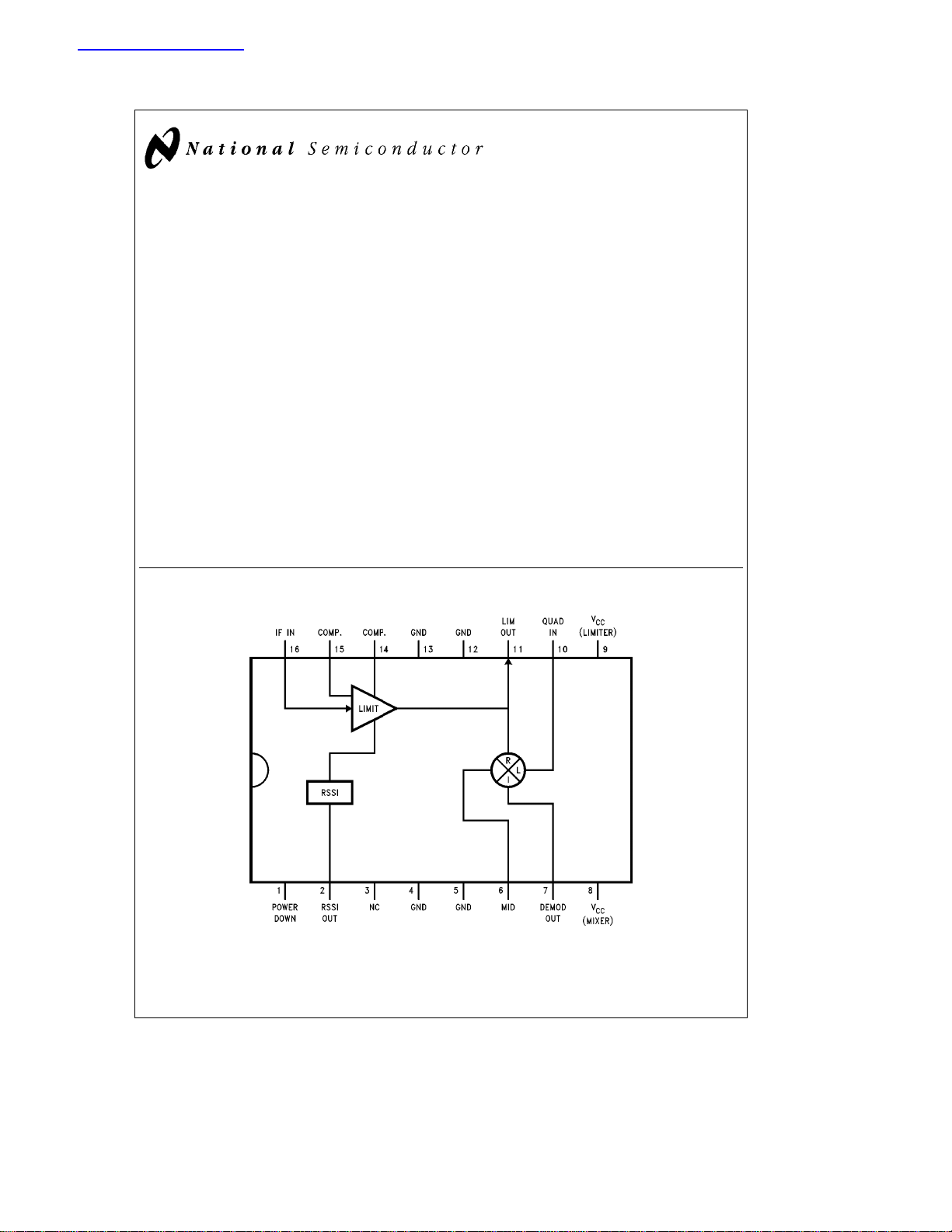
The LMX2240 consists of a high gain limiting amplifier, a
frequency discriminator, and a received signal strength indicator (RSSI). The high gain limiting amplifier and discriminator operate in the 40 MHz to 150 MHz frequency range, and
the limiter has approximately 70 dB of gain. The use of the
limiter and the discriminator provides a low cost, high performance demodulator for communications systems. The
RSSI output can be used for channel quality monitoring.
The LMX2240 is intended to support single conversion receivers. This device saves power, size, and cost by eliminating the second local oscillator (LO), second converter (mixer), and additional filters. The LMX2240 is recommended for
systems with channel bandwidths of 300 kHz to 2.5 MHz.
The LMX2240 is available in a 16-pin JEDEC surface mount
plastic package.
Functional Block Diagram
Features
Y
Typical operation at 110 MHz
Y
RF sensitivity tob75 dBm; RSSI sensitivity to
b
82 dBm
Y
High gain (70 dB) limiting amplifier
Y
Average current consumption: 480 mA for DECT
handset (burst mode)
Y
a
3V operation
Y
Power down mode for increased current savings
Y
Part of a complete receiver solution with the LMX2216
LNA/Mixer, the LMX2315/20 Phase-locked Loop, and
the LMX2411 Baseband Processor
Y
Compliant to ARi
1
TM
specification
Applications
Y
Digital European Cordless Telecommunications (DECT)
Y
Portable wireless communications (PCS/PCN, cordless)
Y
Wireless local area networks (WLANs)
Y
Digital cellular telephone systems
Y
Other wireless communications systems
TL/W/11755– 1
1
ABiCTMand ARi
C
1995 National Semiconductor Corporation RRD-B30M115/Printed in U. S. A.
TM
are trademarks of National Semiconductor Corporation.
TL/W/11755
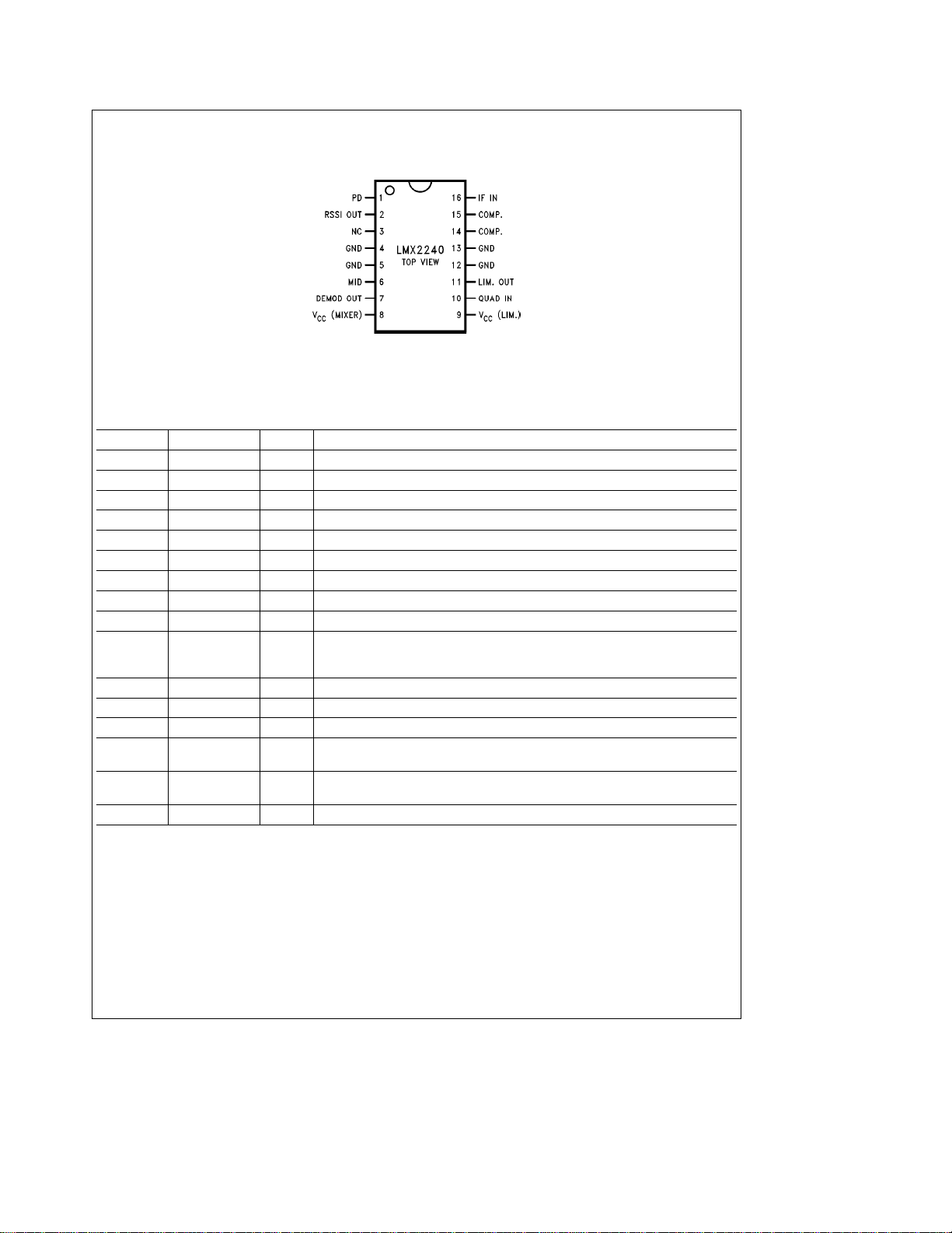
Connection Diagram
Small Outline Package
TL/W/11755– 2
Top View
Order Number LMX2240M
See NS Package Number M16A
Pin Description
Pin No. Pin Name I/O Description
1 PD I Power Down; a HIGH signal switches the part to power down mode.
2 RSSI Out O Voltage output of the received signal strength indicator (RSSI).
3 NC No connection
4 GND Ground
5 GND Ground
6 MID O Mid-range output of the discriminator; can be used for comparator threshold.
7 Demod Out O Demodulated output of the discriminator.
8V
9V
10 Quad In I Quadrature input. A DC path from source through an inductor must be present at
11 Lim. Out O Limiter output to the quadrature tank.
12 GND Ground
13 GND Ground
14 Comp. Compensation pin for the limiter. See Applications Information for capacitor
15 Comp. Compensation pin for the limiter. See Applications Information for capacitor
16 IF In I IF input to the limiter.
(Mixer) Source voltage for the mixer (discriminator).
CC
(Lim.) Source voltage for the limiter.
CC
this pin, but, there must be no series resistance (a parallel resistor to the inductor
is acceptable).
value.
value.
2
Absolute Maximum Ratings
If Military/Aerospace specified devices are required,
please contact the National Semiconductor Sales
Office/Distributors for availability and specifications.
Power Supply Voltage (V
Storage Temperature Range (TS)
Lead Temperature (T
(Soldering, 10 seconds)
) 6.5V
CC
)
L
b
65§Ctoa150§C
a
260§C
Recommended Operating
Conditions
Supply Voltage (V
3V 2.85 3.15 V
CC
)
Operating Temperature (T
Min Max Units
b
)
A
10
a
70
C
§
Electrical Characteristics
The following specifications apply for supply voltage V
specified
Symbol Parameter Conditions Min
I
DD
Supply Current 810mA
CC
ea
3Vg5%, f
e
120 MHz, and T
IN
e
25§C unless otherwise
A
Value
Typ
Max Units
IPDPower Down Current 115 200 mA
f
f
max
min
Maximum IF Input Frequency 120 150 MHz
Minimum IF Input Frequency 10 MHz
IF LIMITER
NF IF Limiter Noise Figure 11.5 12.5 dB
A
V
Limiter Gain Z
sens Limiter/Disc. Sensitivity BERe0.001
IF
in
IF
out
V
max
V
out
IF Limiter Input Impedance 150 225 X
IF Limiter Output Impedance 250 X
Maximum Input Voltage Level 500 mV
Output Swing 350 500 V
Lim Input Limiting Point
e
1000X 70 dB
L
b
75 dBm
b
70 dBm
DISCRIMINATOR
V
out
V
OS
Discriminator Output Peak-to-Peak Voltage See Test Circuit 1.0 1.2 V
(Note 1)
Disc. Output DC Voltage (Pin 7) 1.4 1.7 V
MID Mid-Range Output (Pin 6) 1.4 1.7 V
DISC
DISC
Disc. Input Impedance 1000 X
in
Disc. Output Impedance 150 X
out
RSSI
RSSI RSSI Dynamic Range 70 dB
RSSI
RSSI Output Voltage Pineb80 dBm 0.35 0.5 0.8 V
out
Pine0 dBm 1.15 1.5 1.8 V
RSSI Slope Pineb70 dBm tob20 dBm 11 16 mV/dB
RSSI Linearity 3dB
Note 1: The discriminator output peak-to-peak voltage is measured by operating the discriminator mixer with two separate inputs (i.e., as a mixer). A beat frequency
of 1 kHz is generated, and this tone’s output swing is guaranteed to be at least 1.0 V
circuit, the guaranteed 1.0 V
interest from the tank circuit.
output translates to (1.0V *(36/180)e) 200 mVPPdemodulated output, assuming at least 36§phase shift across the band of
PP
. When the mixer is configured as a discriminator with the limiter and a tank
PP
PP
PP
PP
3
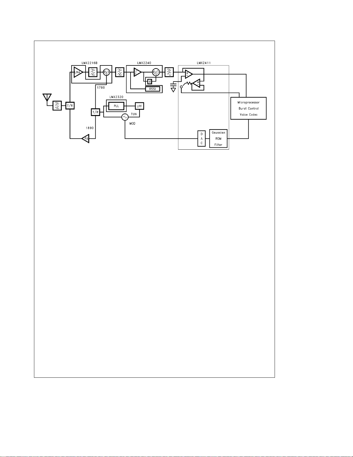
Typical Application Block Diagram
Functional Description
OVERVIEW
The LMX2240 IF demodulator is a low power IF processor
that includes a frequency discriminator, an IF hard limiting
amplifier, and a received signal strength indicator (RSSI).
The LMX2240 is capable of differentially demodulating an
FM or AM signal with as high an IF as 150 MHz, avoiding a
costly second down-conversion. The RSSI output can be
used for time gated channel measurements required in
TDMA and other systems. Other features include high receiver sensitivity and a power down mode to allow for standby operation.
THE LIMITING AMPLIFIER
The limiting amplifier has a typical gain of 70 dB and a sensitivity of about
DECT system with 20 dB net RF gain in front of it to achieve
a sensitivity of
with internal compensation at each stage to ensure stability.
Two external compensation capacitors are also required to
further enhance stability. The input to the limiter is a relatively low impedance to allow easy matching to typical IF surface acoustic wave (SAW) filters. The output of the limiter is
connected off chip to an external quadrature tank circuit as
well as connected internally to the discriminator (mixer). The
output impedance of the limiter is 250X (typical).
b
75 dBm. This allows it to be used in the
b
95 dBm. The limiter is a five stage amplifier
TL/W/11755– 3
THE RECEIVED SIGNAL STRENGTH INDICATOR (RSSI)
The RSSI circuit has a range of 70 dB. Its output voltage is
proportional to the logarithm of the input signal level. The
RSSI circuit has a sensitivity of
age of the circuit ranges from 0.5V to 1.5V typically.
THE FREQUENCY DISCRIMINATOR
The frequency discriminator is a Gilbert cell mixer that requires an external tank circuit to create a 90
the desired frequency. The output of this circuit is centered
at 1.5V by an internal level shifting circuit, and a mid-range
voltage (at 1.5V) is also provided. The sensitivity of the discriminator to phase inaccuracies is 5.5 mV/degree (see Applications Information). This means that for a phase imbalance of 10
about 55 mV off of the 1.5V mid-range voltage. For the typical case, this amounts to about 10% of the output eye diagram (for 400 mV
, the received eye diagram will be shifted by
§
output).
PP
b
82 dBm. The output volt-
phase shift at
§
4

Typical Performance Characteristics
Limiter Gain vs Frequency with
Temperature as a Parameter
Limiter Gain vs Frequency with
Supply Voltage as a Parameter
TL/W/11755– 4
TL/W/11755– 5
5

Typical Performance Characteristics (Continued)
Discriminator Output Peak-to-Peak Voltage
vs Supply with Temperature as a Parameter
TL/W/11755– 6
Mid-Range (Reference) Voltage vs Supply
with Temperature as a Parameter
Current Consumption vs Supply Voltage
with Temperature as a Parameter
TL/W/11755– 7
Power Down Current vs Temperature
Limiter Output Power vs Frequency
with Voltage as a Paramerer
TL/W/11755– 8
TL/W/11755– 10
TL/W/11755– 9
Limiter Output Power vs Frequency
with Temperature as a Paramerer
TL/W/11755– 11
6

Typical Performance Characteristics (Continued)
RSSI Output vs Input Power
with V
as a Parameter
CC
RSSI Output vs Input Power with
Temperature as a Parameter
TL/W/11755– 12
TL/W/11755– 13
7

Automatic Test Circuit
C1e1000 pFg10% NPO Ceramic
e
C3
1000 pFg10% NPO Ceramic
e
R2
1kXg5% (/4W Thin Film Carbon
e
L1
10 mHg5% Air Coil
e
g
R4
20X
5% (/4W Thin Film Carbon
e
R5
3.9 kXg5% (/4W Thin Film Carbon
e
1000 pFg10% NPO Ceramic
C2
e
R1
25Xg5% (/4W Thin Film Carbon
e
R3
1kXg5% (/4W Thin Film Carbon
e
C4
1000 pFg10% NPO Ceramic
e
1000 pF
g
10% NPO Ceramic
C5
TL/W/11755– 14
8

Typical Application Example
C1eC2eC3eC5eC6e100 pFg10% NPO Ceramic
e
1pFg10% NPO Ceramic
C4
e
C8
82 pFg10% X7R Ceramic
e
R2
880Xg5% (/4W Thin Film Carbon
All supporting components 0603 surface mount except tank.
eC9e
C7
R1
Tank
0.01 mFg10% NPO Ceramic
e
4kXg5% (/4W Thin Film Carbon
e
TokoÝ638AH-0294
TL/W/11755– 15
9

Applications Information
THE INTERMEDIATE FREQUENCY LIMITER
The IF limiter has a large amount of gain at high enough
frequency to cause concern about oscillation. To ensure
that the limiter does not oscillate, a few precautions should
be taken. The compensation capacitors that are used
should be chosen to roll off any unwanted frequencies below the band of interest. The capacitor should be a high Q,
RF type ceramic chip capacitor. For DECT, the capacitor
value should be 100 pF, and the capacitors should be soldered as close to the LMX2240 as possible. This will create
a pass band from 40 MHz to 150 MHz. The AC coupling
capacitor at the input to the limiter (from the SAW filter)
should be the same value as the compensation capacitors.
THE DISCRIMINATOR
There are two types of discriminator that can be used to
demodulate FM signals. The first is a delay line discriminator, which uses a delay in one path of the received signal to
introduce a phase difference between it and the received
signal. The operation of the delay line discriminator is derived in the inset box. The other type of discriminator relies
on a quadrature tank to directly introduce a phase shift in
the received signal. This is the type of implementation that
is commonly used in mobile communications because of its
relative ease of construction and low cost.
The discriminator operates best when the inputs to it are
hard-limited (i.e., square edges). If the input signal is small
enough such that the IF amplifier cannot limit it, the output
voltage swing of the limiter will suffer. Typically, the minimum voltage swing the discriminator can see and still fully
switch is about 100 mV
tor can be of different peak-to-peak voltage swings as long
as both are over the lower limit. This allows the quadrature
tank circuit to have some insertion loss. In fact, up to 8 dB
insertion loss can be tolerated while still ensuring that the
discriminator output won’t suffer.
The quadrature circuit can also affect the discriminator output voltage swing. The discriminator output voltage swing
specified assumes perfect quadrature at the frequency of
interest (mixer operation). With available analog components, perfect quadrature is not possible. This is due in part
to the high frequency of the IF and the proportionally very
narrow bandwidth of the desired signal. For example, a
DECT signal is about 1 MHz wide, which is
at which the demodulation occurs. This makes the quadrature circuit difficult to achieve. With moderately high Q components, however, a reasonable phase shift can be
achieved with a single pole tank. This is illustrated by the
following equation: the output of the discriminator is given
by
which results in
When the double frequency component is filtered out with a
low pass filter, the cosine of the phase remains
It can be seen that at 90§phase shift, the output will be zero.
At 0
output swing is then set by the multiplication of the cosine
term with the discriminator output amplifier’s gain.
e
cos(0
out
, the output will be 0.5, and at 180§, it will beb0.5. The
§
. The two inputs to the discrimina-
PP
e
cos(0
t
out
c
out
)#cos(0
c
a
aw)a
t
0
t
c
e
cos(bw)ecos(w).
cos(0
k
a
t
c
t
c
1% of the IF
w),
b
b
0
t
c
w).
(1)DISC
(2)DISC
(3)DISC
With a circuit that gives an output peak-to-peak voltage of
1.0 V
(min) with ideal quadrature, the slope is seen to be
PP
5.5 mV/degree. With a practical quadrature tank circuit at
110.6 MHz, the phase shift over a 1 MHz bandwidth is about
45
–50§, which translates to an output peak-to-peak voltage
§
of about 250 mV
Assume the FM modulated signal is denoted as
e
s(t)
where m(t)em
and b(t) is the modulating baseband signal. The constant m is defined as m
be delayed by some
l(t)es(t
If the delay u is such that
e
0ct
then s(t
and multiplying (4) and (7) yields
s(t) l(t)ecos (0ctam(t)) sin (0ctam(t
The double frequency component can be filtered off
with a lowpass filter. If
1
sin (m(t
2
The object for a delay line, then, is to maximize the delay while retaining the approximations necessary to satisfy (9),
.
PP
cos (0ctam(t)) , (4)
t
b(t) dt ,
b%
#
e
2DfTb. The signal s(t) must
u so that
au)e
2nq
au)e
1
e
2
a
q
a
2
sin(0ctam(t
sin (2
1
sin (m(t
2
cos (0c(t
,n
a
0ct
au)a
m(t
e
0, 1, 2, 3, . . . ,
a
u)), (7)
m(t)am(t
au)b
m(t)) .
a
u)) . (5)
a
u))
a
u))
u is kept small,
1
m(t))
&
e
e
&
au)b
[
m(t
2
a
t
u
m
b%
2
#
t
m
b%
2
#
a
t
u
m
2
#
t
m
b(t) .
u
2
]
m(t)
b
b(t) dt
b(t) dt (9)
b(t) dt
u
au)b
k
0.1 Tb.
(6)
(8)
10

11

Physical Dimensions inches (millimeters)
LMX2240 Intermediate Frequency Receiver
For Tape and Reel Order Number LMX2240MX
16-Lead Molded Package (SO)
Order Number LMX2240M
NS Package Number M16A
LIFE SUPPORT POLICY
NATIONAL’S PRODUCTS ARE NOT AUTHORIZED FOR USE AS CRITICAL COMPONENTS IN LIFE SUPPORT
DEVICES OR SYSTEMS WITHOUT THE EXPRESS WRITTEN APPROVAL OF THE PRESIDENT OF NATIONAL
SEMICONDUCTOR CORPORATION. As used herein:
1. Life support devices or systems are devices or 2. A critical component is any component of a life
systems which, (a) are intended for surgical implant support device or system whose failure to perform can
into the body, or (b) support or sustain life, and whose be reasonably expected to cause the failure of the life
failure to perform, when properly used in accordance support device or system, or to affect its safety or
with instructions for use provided in the labeling, can effectiveness.
be reasonably expected to result in a significant injury
to the user.
National Semiconductor National Semiconductor National Semiconductor National Semiconductor
Corporation Europe Hong Kong Ltd. Japan Ltd.
1111 West Bardin Road Fax: (
Arlington, TX 76017 Email: cnjwge@tevm2.nsc.com Ocean Centre, 5 Canton Rd. Fax: 81-043-299-2408
Tel: 1(800) 272-9959 Deutsch Tel: (
Fax: 1(800) 737-7018 English Tel: (
National does not assume any responsibility for use of any circuitry described, no circuit patent licenses are implied and National reserves the right at any time without notice to change said circuitry and specifications.
Fran3ais Tel: (
Italiano Tel: (
a
49) 0-180-530 85 86 13th Floor, Straight Block, Tel: 81-043-299-2309
a
49) 0-180-530 85 85 Tsimshatsui, Kowloon
a
49) 0-180-532 78 32 Hong Kong
a
49) 0-180-532 93 58 Tel: (852) 2737-1600
a
49) 0-180-534 16 80 Fax: (852) 2736-9960
 Loading...