

查询LMX2216供应商
LMX2216
0.1 GHz to 2.0 GHz Low Noise Amplifier/Mixer
for RF Personal Communications
General Description
The LMX2216 is a monolithic, integrated low noise amplifier
(LNA) and mixer suitable as a first stage amplifier and downconverter for RF receiver applications. The wideband operating capabilities of the LMX2216 allow it to function over
frequencies from 0.1 GHz to 2.0 GHz. It is fabricated using
National Semiconductor’s ABiC IV BiCMOS process.
All input and output ports of the LMX2216 are single-ended.
The LNA input and output ports are designed to interface to
a50Xsystem. The Mixer input ports are matched to 50X.
The output port is matched to 200X. The only external components required are DC blocking capacitors. The balanced
architecture of the LMX2216 maintains consistent operating
parameters from unit to unit, since it is implemented in a
monolithic device. This consistency provides manufacturers
a significant advantage since tuning proceduresÐoften
needed with discrete designsÐcan be reduced or eliminated.
The low noise amplifier produces very flat gain over the entire operating range. The doubly-balanced, Gilbert-cell mixer
provides good LO-RF isolation and cancellation of secondorder distortion products. A power down feature is implemented on the LMX2216 that is especially useful for standby operation common in Time Division Multiple Access
(TDMA) and Time Division Duplex (TDD) systems.
August 1995
The LMX2216 is available in a narrow-body 16-pin surface
mount plastic package.
Features
Y
Wideband RF operation from 0.1 GHz to 2.0 GHz
Y
No external biasing components necessary
Y
3V operation
Y
LNA input and output ports matched to 50X
Y
Mixer input ports matched to 50X, output port matched
to 200X.
Y
Doubly balanced Gilbert cell mixer (single ended input
and output)
Y
Low power consumption
Y
Power down feature
Y
Small outline, plastic surface mount package
Applications
Y
Digital European Cordless Telecommunications (DECT)
Y
Portable wireless communications (PCS/PCN, cordless)
Y
Wireless local area networks (WLANs)
Y
Digital cellular telephone systems
Y
Other wireless communications systems
LMX2216 0.1 GHz to 2.0 GHz Low Noise Amplifier/Mixer for RF Personal Communications
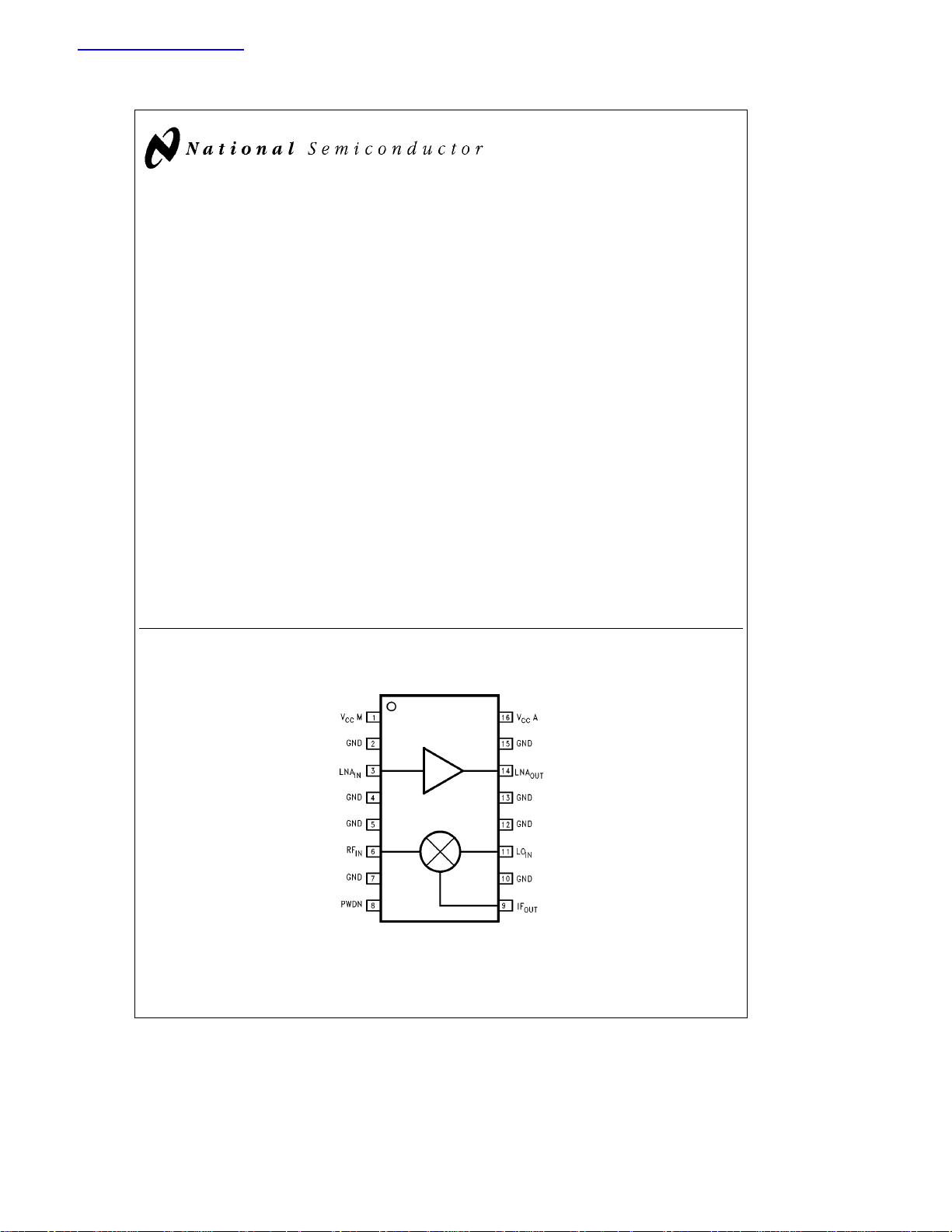
Functional Block/Pin Diagram
Order Number LMX2216M
See NS Package Number M16A
C
1995 National Semiconductor Corporation RRD-B30M115/Printed in U. S. A.
TL/W/11814
TL/W/11814– 1

Pin Description
Pin Pin
No. Name
1VCCM I Voltage supply for the mixer. The input voltage level to this pin should be a DC Voltage ranging from
2 GND Ground
3 LNA
4 GND Ground
5 GND Ground
6RFINI RF input to the mixer. The RF signal to be down converted is connected to this pin. External DC
7 GND Ground
8 PWDN I Power down signal pin. Both the LNA and mixer are powered down when a HIGH level is applied to
9IF
OUT
10 GND Ground
11 LO
12 GND Ground
13 GND Ground
14 LNA
15 GND Ground
16 VCCA I LNA supply Voltage. DC Voltage ranging from 2.85V to 3.15V.
I/O Description
2.85V to 3.15V.
IN
IN
OUT
I RF input signal to the LNA. External DC blocking capacitor is required.
blocking capacitor is required.
this pin (VIH).
O IF output signal of the mixer. External DC blocking capacitor is required.
I Local oscillator input signal to the mixer. External DC blocking capacitor is required.
O Output of the LNA. This pin outputs the amplified RF signal. External DC blocking capacitor is
required.
Absolute Maximum Ratings
If Military/Aerospace specified devices are required,
please contact the National Semiconductor Sales
Office/Distributors for availability and specifications.
Supply Voltage (V
Storage Temperature (T
Operating Temperature (TO)
) 6.5V
CC
)
S
b
65§Ctoa150§C
b
40§Ctoa85§C
Recommended Operating
Conditions
Supply Voltage (VCC) 2.85V–3.15V
Operating Temperature (T
RF
IN
LO
IN
2
)
A
b
10§Ctoa70§C
0.1 GHz to 2.0 GHz
0.1 GHz to 2.0 GHz

Electrical Characteristics: LNA
ea
(V
CC
3.0Vg5%, T
e
A
25§C, Z
e
o
50X and f
e
IN
Symbol Parameter Conditions Min Typ Max Units
I
CC
I
CC-PWDN
Supply Current In Operation 6.5 8.0 mA
Supply Current In Power Down Mode 10 mA
G Gain 910 dB
P
1dB
Output 1 dB Compression Point
OIP3 Output 3rd Order Intercept Point 5.0 7.0 dBm
NF Single Side Band Noise Figure 4.8 6.0 dB
RL
RL
IN
OUT
Input Return Loss 10 15 dB
Output Return Loss 10 11 dB
2.0 GHz
@
b
30 dBm unless otherwise specified.)
b
5.0b3.0 dBm
Electrical Characteristics: Mixer (V
b
30 dBm, f
e
1.89 GHz@0 dBm; f
LO
e
110 MHz unless otherwise specified.)
IF
CC
ea
3.0Vg5%, T
e
25§C, Z
A
e
50X,f
o
e
2.0 GHz
RF
Symbol Parameter Conditions Min Typ Max Units
I
CC
I
CC-PWDN
G
C
P
1dB
OIP3 Output Third Order Intercept Point
Supply Current In Operation 9.0 12.0 mA
Supply Current In Power Down Mode 10 mA
Conversion Gain (Single Side Band) 4.0 6.0 dB
Output 1 dB Compression Point
b
b
b
13.0
9.0 dBm
3.0 0.0 dBm
SSB NF Single Side Band Noise Figure 17 18 dB
DSB NF Double Side Band Noise Figure 14 15 dB
LO-RF LO to RF Isolation 20 30 dB
LO-IF LO to IF Isolation 20 30 dB
RF RL RF Return Loss 10 15 dB
LO RL LO Return Loss 10 15 dB
IF RL IF Return Loss 15 dB
Z
IF
IF Port Impedance 200 X
Electrical Characteristics: Power Down
Symbol Parameter Conditions Min Typ Max Units
V
IH
V
IL
I
IH
I
IL
High Level Input Voltage V
Low Level Input Voltage 0.8 V
High Level Input Current V
Low Level Input Current V
e
V
IH
CC
e
GND
IL
b
0.8 V
CC
b
10.0 10.0 mA
b
10.0 10.0 mA
@
3
Typical Application Block Diagram
Typical Characteristics
LNA
LNA Current Composition
vs Supply Voltage with
Temperature as a Parameter
LNA P
Temperature as a Parameter
OUT
vs PINwith
TL/W/11814– 3
FIGURE 2
LNA P
Voltage as a Parameter
LNA P
Temperature as a Parameter
vs PINwith Supply
OUT
vs PINwith
OUT
TL/W/11814– 2
TL/W/11814– 4
TL/W/11814– 6
TL/W/11814– 7
4
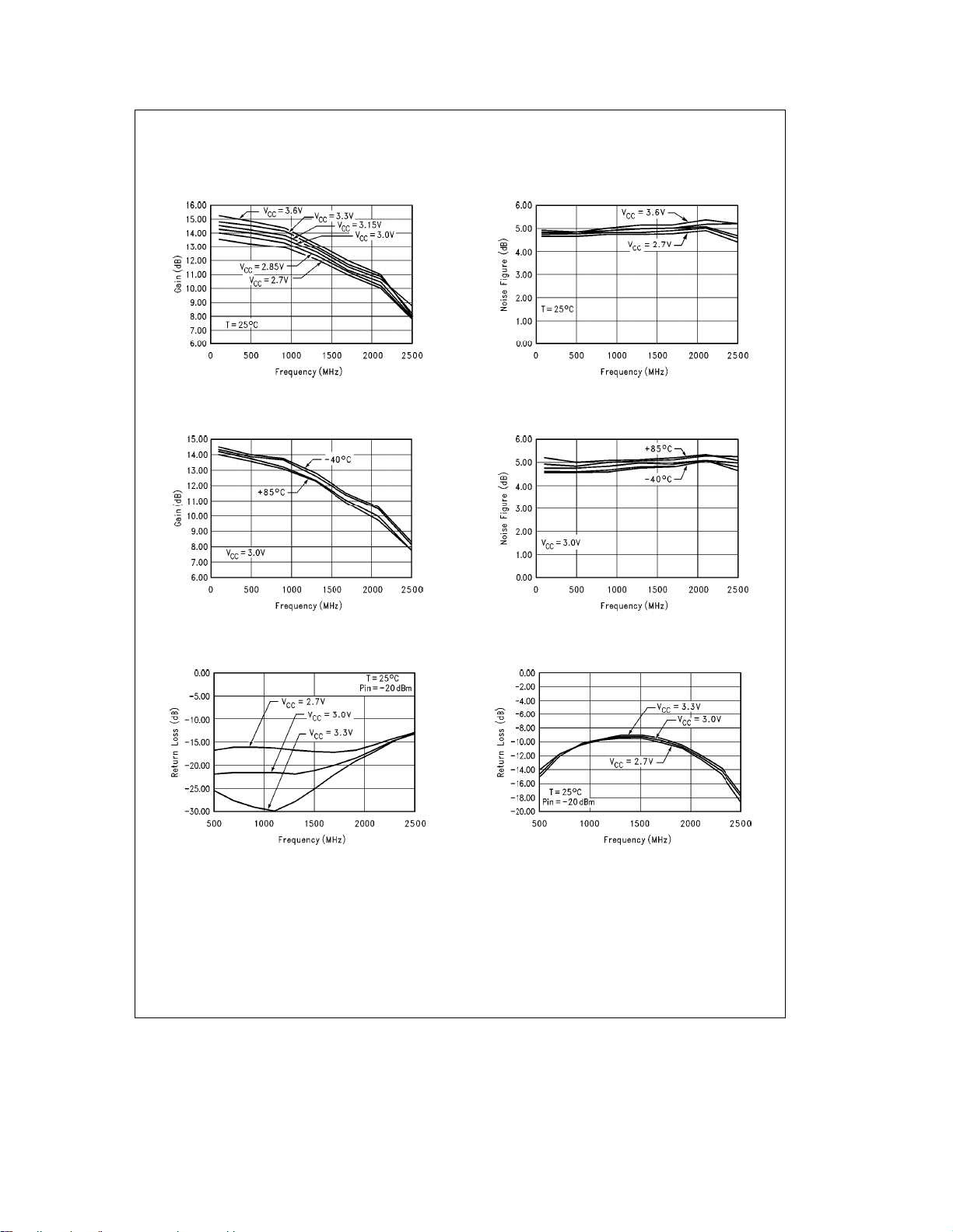
Typical Characteristics (Continued)
LNA (Continued)
LNA Gain vs Frequency with Supply
Voltage as a Parameter
LNA Noise Figure vs Frequency with
Supply Voltage as a Parameter
LNA Gain vs Frequency with
Temperature as a Parameter
TL/W/11814– 10
LNA Input Return Loss vs Frequency
with Voltage as a Parameter
TL/W/11814– 8
TL/W/11814– 9
LNA Noise Figure vs Frequency with
Temperature as a Parameter
TL/W/11814– 11
LNA Output Return Loss vs Frequency
with Voltage as a Parameter
TL/W/11814– 12
TL/W/11814– 19
5

Typical Characteristics (Continued)
MIXER
Mixer Gain (Double Sideband)
vs Frequency with Supply
Voltage as a Parameter
Mixer Gain (Double Sideband)
vs Frequency with Temperature
as a Parameter
TL/W/11814– 20
Mixer Noise Figure (Double Sideband)
vs Frequency with Supply
Voltage as a Parameter
TL/W/11814– 22
TL/W/11814– 21
Mixer Noise Figure (Double Sideband)
vs Frequency with Temperature
as a Parameter
TL/W/11814– 23
6

Typical Characteristics (Continued)
MIXER (Continued)
Mixer P
Voltage as a Parameter
vs PINwith Supply
OUT
Mixer P
Voltage as a Parameter
vs PINwith Supply
OUT
Mixer P
Temperature as a Parameter
OUT
vs PINwith
Mixer RFINReturn Loss
vs Frequency with Supply
Voltage as a Parameter
TL/W/11814– 24
TL/W/11814– 26
Mixer P
Temperature as a Parameter
OUT
vs PINwith
Mixer RFINReturn Loss
vs Frequency with Supply
Voltage as a Parameter
TL/W/11814– 25
TL/W/11814– 27
TL/W/11814– 28
TL/W/11814– 29
7
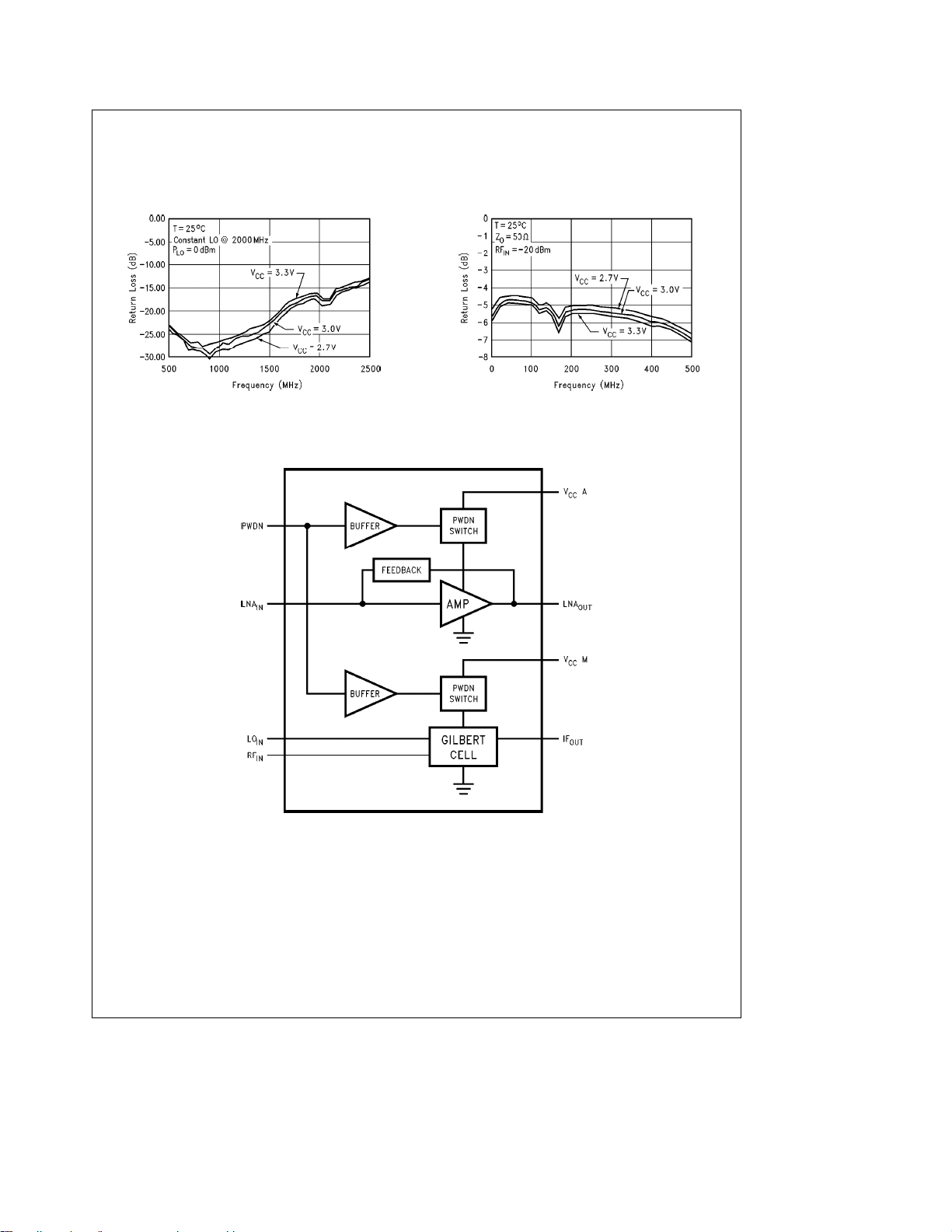
Typical Characteristics (Continued)
MIXER (Continued)
Mixer RF
vs Frequency with Supply
Voltage as a Parameter
Return Loss
IN
Mixer IF
vs Frequency with Supply
Return Loss
OUT
Voltage as a Parameter
Functional Description
TL/W/11814– 30
FIGURE 3. Block Diagram of the LMX2216
TL/W/11814– 31
TL/W/11814– 13
8

Functional Description (Continued)
THE LNA
The LNA is a common emitter stage with active feedback.
This feedback network allows for wide bandwidth operation
while providing the necessary optimal input impedance for
low noise performance. The power down feature is implemented using a CMOS buffer and a power-down switch. The
power down switch is implemented with CMOS devices.
During power down, the switch is open and only leakage
currents are drawn from the supply.
THE MIXER
The mixer is a Gilbert cell architecture, with the RF input
signal modulating the LO signal and single ended output
taken from the collector of one of the upper four transistors.
The power down circuitry of the mixer is similar to that of the
LNA. The power down switch is used to provide or cut off
bias to the Gilbert cell.
Typical Low Noise Amplifier
Typical Gilbert Cell
(B
ON
TL/W/11814– 14
2
b
]
BG)
FIGURE 4. Typical LNA Structure
A typical low noise amplifier consists of an active amplifying
element and input and output matching networks. The input
matching network is usually optimized for noise performance, and the output matching network for gain. The active
element is chosen such that it has the lowest optimal noise
figure, F
figure of a linear two-port is a function of the source admittance and can be expressed by
where G
, an intrinsic property of the device. The noise
MIN
R
MIN
a
n
a
[
(G
ON
G
G
e
jB
a
R
n
generator admittance presented to
G
the input of the two port,
e
jB
generator admittance at which op-
ON
timum noise figure occurs,
e
empirical constant relating the
sensitivity of the noise figure to
generator admittance.
e
F
F
G
G
ON
2
b
a
GG)
FIGURE 5. Typical Gilbert Cell Circuit Diagram
The Gilbert cell shown above is a circuit which multiplies
two input signals, RF and LO. The input RF voltage differentially modulates the currents on the collectors of the transistors Q1 and Q2, which in turn modulate the LO voltage by
varying the bias currents of the transistors Q3, Q4, Q5, and
Q6. Assuming that the two signals are small, the result is a
product of the two signals, producing at the output a sum
and difference of the frequencies of the two input signals. If
either of these two signals are much larger than the threshold voltage V
and higher order terms which are undesirable and may need
to be attenuated or filtered out.
Analysis of the Gilbert cell shows that the output, which is
the difference of the collector currents of Q3 and Q6, is
related to the two inputs by the equation:
DI
and the hyperbolic tangent function can be expressed as a
Taylor series
Assuming that the RF and LO signals are sinusoids.
then
DIeI
The lowest order term is a product of two sinusoids, yielding
a sum of two sinusoids,
one of which is the desired intermediate frequency signal.
, the output will contain other mixing products
T
V
e
b
I
I
C3
C6
tanh(x)
V
V
Acos (0RFtawRF)
EE
Ð
Bcos (0LOtawLO)
#
Ð
AB
cos ((0
I
EE
a
2
Ð
e
I
EE
exb
e
Acos (0RFtawRF)
RF
e
Bcos (0LOtawLO)
LO
a
RF
cos ((0
RF
Ð
tanh
b
0
b
RF
2V
#
T
3
5
x
x
a
3
5
3
A
3
b
cos
3
3
B
3
cos
(0LOtawLO)a...
3
)taw
LO
0
)taw
LO
TL/W/11814– 15
V
LO
tanh
...
RF
2V
#
T
a
wLO)
b
wLO)
(
J( Ð
b
(0RFtawRF)a...
RF
J(
(
(
9
Figures of Merit
GAIN (G)
Many different types of gain are specified in RF engineering.
The type referred to here is called transducer gain and is
defined as the ratio of the power delivered to the load to the
available power from the source,
P
e
G
P
where V
generator voltage with internal resistance R
is the voltage across the load RLand VINis the
OUT
scattering parameters, transducer gain is defined as
where S21is the forward transmission parameter, which can
be measured using a network analyzer.
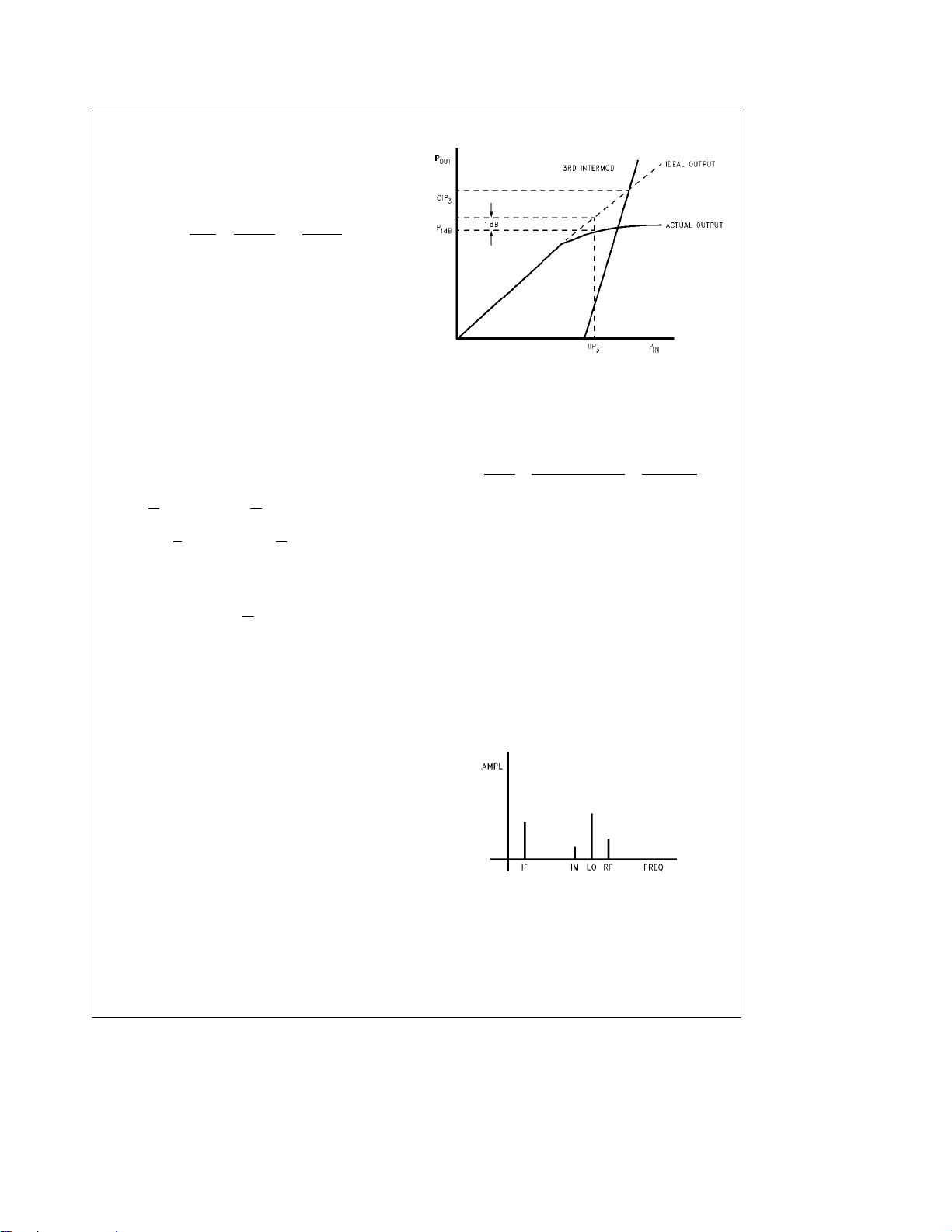
1 dB COMPRESSION POINT (P
A measure of amplitude Iinearity, 1 dB compression point is
the point at which the actual gain is 1dB below the ideal
linear gain. For a memoryless two-port with weak nonlinearity, the output can be represented by a power series of the
input as
e
v
o
For a sinusoidal input,
the output is
1
e
v
o
2
a
k
A
2
2
1
a
k
2
2
assuming that all of the fourth and higher order terms are
negligible. For an amplifier, the fundamental component is
the desired output, and it can be rewritten as
k
This fundamental component is larger than k
linear gain) if k
cal devices, k
tude A of the input signal gets larger. The 1 dB compression
l
3
k
3
point can be expressed in terms of either the input power or
the output power. Measurement of P
increasing the input power while observing the output power
until the gain is compressed by 1 dB.
THIRD ORDER INTERCEPT (OIP
Third order intercept is another figure of merit used to characterize the linearity of a two-port. It is defined as the point
at which the third order intermodulation product equals the
ideal linear, uncompressed, output. Unlike the P
involves two input signals. However, it can be shown mathematically (similar derivation as above) that the two are
closely related and OIP
figures of merit are illustrated in
2
V
/R
OUT
OUT
e
IN
e
G
a
k1v
i
v
k1A
#
A2cos 201t
AÐ1
1
2
V
IN
20 log (lS
k2v
e
Acos 01t
i
a
3
a
4
/R
3
4
2
i
(k
S
1dB
a
k
a
3/k1
L
k3v
A
3
1
4
0 and smaller if k
0, and the gain compresses as the ampli-
)
3
&
P
3
1dB
Figure 6
2
R
V
OUT
S
e
4
2
RLV
IN
. In terms of
S
)
l
21
)
3
a
...
i
3
cos 01t
J
k
A3cos 301t
3
2
)A
.
(
A (the ideally
1
k
0. For most practi-
3
can be made by
1dB
a
10 dB. Theses two
.
1dB
, OIP
FIGURE 6. Typical P
OUT–PIN
Characteristics
NOISE FIGURE (NF)
Noise figure is defined as the input signal to noise ratio divided by the output signal to noise ratio. For an amplifier, it
can also be interpreted as the amount of noise introduced
by the amplifier itself seen at the output. Mathematically,
Si/N
i
e
F
So/N
e
o
GaSi/(N
Si/N
a
a
i
GaNi)
NFe10 log (F)
and Nirepresent the signal and noise power levels
where S
i
available at the input to the amplifier, S
and noise power levels available at the output, G
able gain, and Na the noise added by the amplifier. Noise
figure is an important figure of merit used to characterize the
performance of not only a single component but also the
entire system. It is one of the factors which determine the
system sensitivity.
IMAGE FREQUENCY, DSB/SSB NF
Image frequency refers to that frequency which is also
down-converted by the mixer, along with the desired RF
component, to the intermediate frequency. This image frequency is located at the same distance away from the LO,
but on the opposite side of the RF. For most mixers, it must
be filtered out before the signal is down-converted; otherwise, an image-reject mixer must be used.
trates the concept.
3
FIGURE 7. Input and Output Spectrum of Mixers
TL/W/11814– 16
a
N
GaN
a
e
GaN
i
and Nothe signal
o
the avail-
a
Figure 7
TL/W/11814– 17
i
illus-
10

Figures of Merit (Continued)
Due to the presence of image frequencies and the method
in which noise figure is defined, noise figures can be measured and specified in two ways: double side band (DSB) or
single side band (SSB). In DSB measurements, the image
frequency component of the input noise source is not filtered and contributes to the total output noise at the intermediate frequency. In SSB measurements. the image frequency is filtered and the output noise is not caused by this
frequency component. In most mixer applications where
only one side band is wanted, SSB noise figure is 3 dB
higher
than DSB noise figure.
In this application, the LMX2216 is used in a radio receiver
front end, where it amplifies the signal from the antenna and
then down converts it to an intermediate frequency. The
image filter placed between the LNA and the mixer attenu-
ates the image frequency. The mixer is shown to use an LO
signal generated by a PLL synthesizer, but, depending on
the type of application, the LO signal could be generated by
a device as simple as a free-running oscillator. The IF output
is then typically filtered by a channel-select filter following
the mixer, and this signal can then be demodulated or go
through another down conversion, depending upon the intermediate frequency and system requirements. This external filter rejects adjacent channels and also attenuates any
LO feed through. Figure 9 shows a cascade analysis of a
typical RF front-end subsystem in which the LMX2216 is
used. It includes the bandpass filter and the switch through
which the input RF signal goes in a radio system before
reaching the LNA. Typical values are used for the insertion
loss of the various filters in this example.
FIGURE 8. Typical Applications Circuit of the LMX2216
Data per Stage Cumulative Data
Ý
Comp Gain N Fig OIP3
1 Filter
2 Switch
b
2.0 2.0 100.0 1
b
0.6 0.6 100.0 2
Ý
Gain N Fig IIP3 OIP3
b
2.0 2.0 97.9 95.9
b
2.6 2.6 96.6 94.0
3 LNA 12.3 3.7 6.0 3 9.7 6.3
4 Filter
b
3.0 3.0 100.0 4 6.7 6.4
5 Mixer 5.8 13.7 3.0 5 12.5 9.6
6 Filter
b
3.0 3.0 100.0 6 9.5 9.7
System Cumulative Values Gain 9.5 dB
N Fig 9.7 dB
b
IIP
OIP
10.5 dBm
3
b
1.0 dBm
3
FIGURE 9. Cascade Analysis Example
11
TL/W/11814– 18
b
3.7 6.0
b
3.7 3.0
b
10.5 2.0
b
10.5
b
1.0
Physical Dimensions inches (millimeters)
JEDEC 16-Lead (0.150×Wide) Small Outline Molded Package (M)
Order Number LMX2216M
For Tape and Reel Order Number LMX2216MX
NS Package Number M16A
LIFE SUPPORT POLICY
NATIONAL’S PRODUCTS ARE NOT AUTHORIZED FOR USE AS CRITICAL COMPONENTS IN LIFE SUPPORT
DEVICES OR SYSTEMS WITHOUT THE EXPRESS WRITTEN APPROVAL OF THE PRESIDENT OF NATIONAL
SEMICONDUCTOR CORPORATION. As used herein:
1. Life support devices or systems are devices or 2. A critical component is any component of a life
systems which, (a) are intended for surgical implant support device or system whose failure to perform can
into the body, or (b) support or sustain life, and whose be reasonably expected to cause the failure of the life
failure to perform, when properly used in accordance support device or system, or to affect its safety or
with instructions for use provided in the labeling, can effectiveness.
be reasonably expected to result in a significant injury
to the user.
National Semiconductor National Semiconductor National Semiconductor National Semiconductor
LMX2216 0.1 GHz to 2.0 GHz Low Noise Amplifier/Mixer for RF Personal Communications
Corporation Europe Hong Kong Ltd. Japan Ltd.
1111 West Bardin Road Fax: (
Arlington, TX 76017 Email: cnjwge@tevm2.nsc.com Ocean Centre, 5 Canton Rd. Fax: 81-043-299-2408
Tel: 1(800) 272-9959 Deutsch Tel: (
Fax: 1(800) 737-7018 English Tel: (
National does not assume any responsibility for use of any circuitry described, no circuit patent licenses are implied and National reserves the right at any time without notice to change said circuitry and specifications.
Fran3ais Tel: (
Italiano Tel: (
a
49) 0-180-530 85 86 13th Floor, Straight Block, Tel: 81-043-299-2309
a
49) 0-180-530 85 85 Tsimshatsui, Kowloon
a
49) 0-180-532 78 32 Hong Kong
a
49) 0-180-532 93 58 Tel: (852) 2737-1600
a
49) 0-180-534 16 80 Fax: (852) 2736-9960
 Loading...