查询LMX2119供应商
LMX2119 1.9 GHz Power Amplifier
LMX2119 1.9 GHz Power Amplifier
General Description
The LMX2119 1.9 GHz Power Amplifier is a monolithic, integrated power amplifier suitable for use in the Digital European Cordless Telecommunications (DECT) system as well as
other mobile telephony and wireless communications applications. It is fabricated using an advanced Gallium Arsenide
technology that allows single supply (
a
3V) operation.
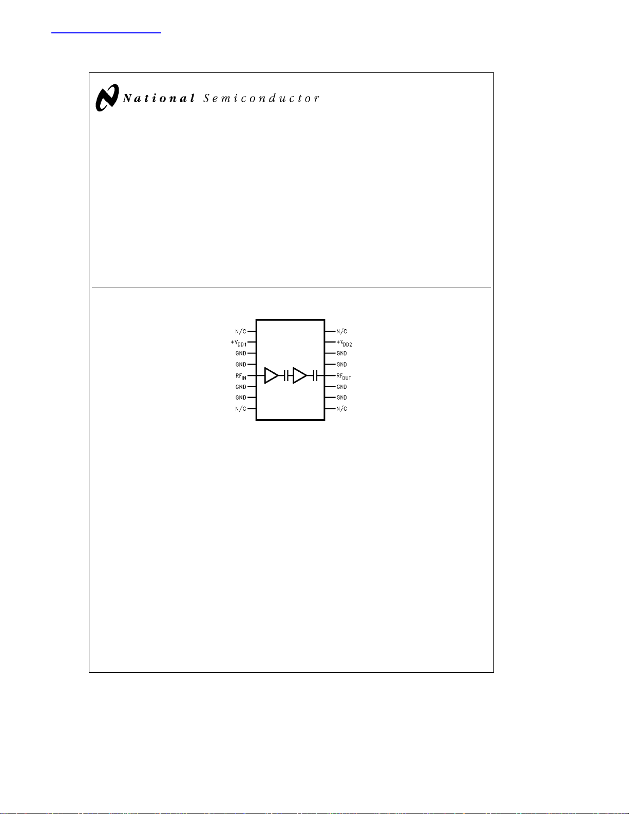
The LMX2119 consists of two MESFETs cascaded to provide 24.5 dB of power gain. The output power at 3.6V is
a
26.5 dBm with an input power level ofa2 dBm. The input
VSWR of the power amplifier remains constant in the ON
and OFF state.
The LMX2119 is available in a 16-pin SOIC surface mount
plastic package.
Functional Block Diagram
Features
Y
Singlea3V supply operation
Y
Class A bias;l30% power added efficiency
Y
24.5 dB power gain;a26.5 dBm output power
Y
50X input/output impedance
Y
350 mA current consumption ata3.6V
Applications
Y
Digital European Cordless Telecommunications (DECT)
Y
Portable wireless communications (PCS/PCN, cordless)
Y
Wireless local area networks (WLANs)
Y
Other wireless communications systems
PRELIMINARY
June 1996
TL/W/12686– 1
This data sheet contains the design specifications for product development.
Specifications may change in any manner without notice.
C
1996 National Semiconductor Corporation RRD-B30M27/Printed in U. S. A.
TL/W/12686
http://www.national.com

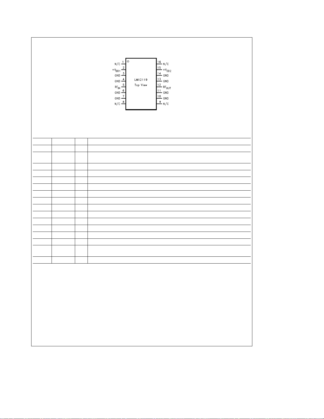
LMX2119 Connection Diagram
Small Outline Package (SOP)
Top View
Order Number LMX2119M
See NS Package Number M16A
Pin Description
Pin No. Pin Name I/O Description
1 N/C No Connect.
2
3 GND Ground.
4 GND Ground.
5 RF In I RF input to the power amplifier.
6 GND Ground.
7 GND Ground.
8 N/C No Connect.
9 N/C No Connect.
10 GND Ground.
11 GND Ground.
12 RF Out O Power amplifier’s RF output.
13 GND Ground.
14 GND Ground.
15
16 N/C No Connect.
a
V
DD1
a
V
DD2
Positive supply voltage. V
close to the pin as possible.
Positive supply voltage. V
close to the pin as possible.
must equal V
DD1
must equal V
DD2
. Decoupling capacitors should be placed as
DD2
. Decoupling capacitors should be placed as
DD1
TL/W/12686– 2
http://www.national.com 2
 Loading...