

查询LMX1600供应商
LMX1600/LMX1601/LMX1602 PLLatinum Low Cost Dual Frequency Synthesizer
LMX1600/LMX1601/LMX1602
PLLatinum
LMX1600 2.0 GHz/500 MHz
LMX1601 1.1 GHz/500 MHz
LMX1602 1.1 GHz/1.1 GHz
General Description
The LMX1600/01/02 is part of a family of monolithic integrated dual frequency synthesizers designed to be used in a
local oscillator subsystem for a radio transceiver. It is fabricated using National’s 0.5uABiCVsilicon BiCMOS process.
The LMX1600/01/02 contains two dual modulus prescalers,
four programmable counters, two phase detectors and two
selectable gain charge pumps necessary to provide the control voltage for two external loop filters and VCO loops. Digital filtered lock detects for both PLLs are included. Data is
transferred into the LMX1600/01/02 via a MICROWIRE
serial interface (Data, Clock, LE).
supply voltage can range from 2.7V to 3.6V. The
V
CC
LMX1600/01/02 features very low current consumption typically 4.0 mA at 3V for LMX1601, 5.0 mA at 3V for
LMX1600 or LMX1602. Powerdown for the PLL is hardware
controlled.
The LMX1600/01/02 is available in a 16 pin TSSOP surface
mount plastic package.
™
Low Cost Dual Frequency Synthesizer
™
PRELIMINARY
March 1998
Features
n VCC= 2.7V to 3.6V operation
n Low current consumption:
@
4mA
3V (typ) for LMX1601
@
5mA
n PLL Powerdown mode: I
n Dual modulus prescaler:
n Digital Filtered Lock Detects
3V (typ) for LMX1600 or LMX1602
— 2 GHz/500 MHz option: (Main) 32/33 (Aux) 8/9
— 1.1 GHz/500 MHz option: (Main) 16/17 (Aux) 8/9
— 1.1 GHz/1.1 GHz option: (Main) 16/17 (Aux) 16/17
= 1 µA typical
CC
Applications
n Cordless / Cellular / PCS phones
n Other digital mobile phones
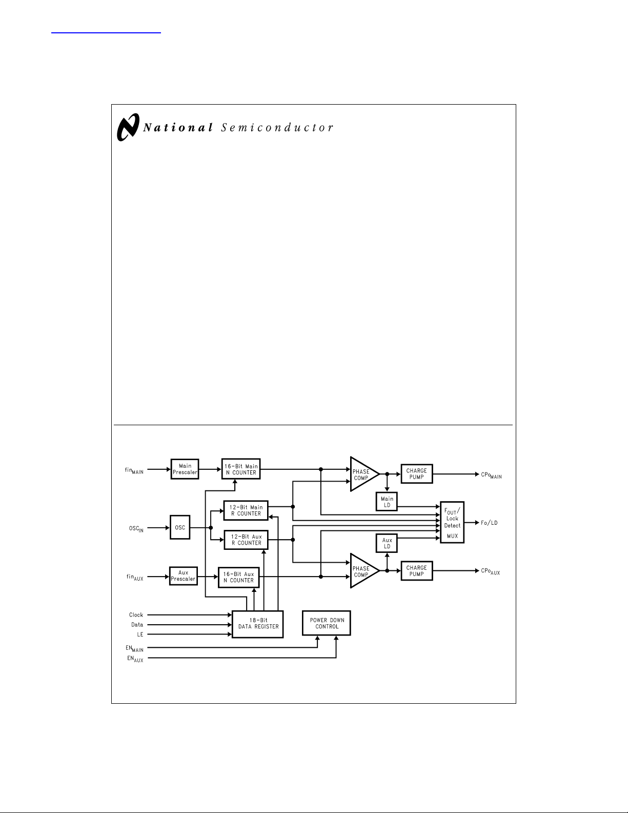
Functional Block Diagram
DS100129-1
TRI-STATE®is a registered trademark of National Semiconductor Corporation.
™
MICROWIRE
© 1998 National Semiconductor Corporation DS100129 www.national.com
and PLLatinum™are trademarks of National Semiconductor Corporation.
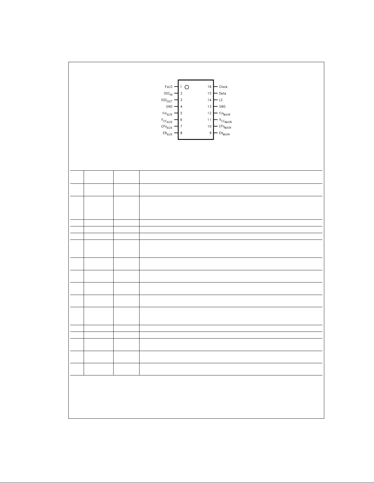
Connection Diagram
DS100129-2
Order Number LMX1600TM, LMX1601TM, or LMX1602TM
NS Package Number MTC16
Pin Description
Pin
Pin Name I/O Description
No.
1 FoLD O Multiplexed output of the Main/Aux programmable or reference dividers and Main/Aux lock
2 OSC
3 OSC
IN
OUT
O Oscillator output. Used with an external resonator.
4 GND — Aux PLL ground.
5 fin
AUX
6V
CC
AUX
7 CPo
8EN
9EN
10 CPo
11 V
12 fin
CC
AUX
AUX
MAIN
MAIN
MAIN
MAIN
— Aux PLL power supply voltage input. Must be equal to V
O Aux PLL Charge Pump output. Connected to a loop filter for driving the control input of an
O Main PLL Charge Pump output. Connected to a loop filter for driving the control input of an
— Main PLL power supply voltage input. Must be equal to V
13 GND — Main PLL ground.
14 LE I Load enable high impedance CMOS input. Data stored in the shift registers is loaded into
15 Data I High impedance CMOS input. Binary serial data input. Data entered MSB first. The last two
16 Clock I High impedance CMOS Clock input. Data for the various counters is clocked in on the
detect. CMOS output. (See Programming Description 2.5)
I PLL reference input which drives both the Main and Aux R counter inputs. Has about 1.2V
input threshold and can be driven from an external CMOS or TTL logic gate. Typically
connected to a TCXO output. Can be used with an external resonator (See Programming
Description 2.5.4).
I Aux prescaler input. Small signal input from the VCO.
. May range from 2.7V to
CC
3.6V. Bypass capacitors should be placed as close as possible to this pin and be
MAIN
connected directly to the ground plane.
external VCO.
I Powers down the Aux PLL when LOW (N and R counters, prescaler, and tristates charge
pump output). Bringing EN
HIGH powers up the Aux PLL.
AUX
I Powers down the Main PLL when LOW (N and R counters, prescaler, and tristates charge
pump output). Bringing EN
HIGH powers up the Main PLL.
MAIN
external VCO.
. May range from 2.7V to
CC
3.6V. Bypass capacitors should be placed as close as possible to this pin and be
AUX
connected directly to the ground plane.
I Main prescaler input. Small signal input from the VCO.
one of the 4 internal latches when LE goes HIGH (control bit dependent).
bits are the control bits.
rising edge, into the 18-bit shift register.
www.national.com 2
Absolute Maximum Ratings (Notes 1, 2)
If Military/Aerospace specified devices are required, please contact the National Semiconductor Sales Office/
Distributors for availability and specifications.
Value
Parameter Symbol Min Typical Max Unit
V
CC
Power Supply Voltage V
Voltage on any pin with GND=0V V
Storage Temperature Range T
Lead Temp. (solder 4 sec) T
MAIN
CC
AUX
I
S
L
−0.3 6.5 V
−0.3 6.5 V
−0.3 VCC+ 0.3 V
−65 +150 ˚C
+260 ˚C
ESD-Human Body Model (Note 2) 2000 eV
Recommended Operating Conditions
Value
Parameter Symbol Min Typical Max Unit
V
CC
Power Supply Voltage V
Operating Temperature T
Note 1: “Absolute Maximum Ratings” indicate limits beyond which damage to the device may occur. Recommended Operating Conditions indicate conditions for
which the device is intended to be functional, but do not guarantee specific performance limits. Electrical Characteristics document specific minimum and/or maximum performance values at specified test conditions and are guaranteed. Typical values are for informational purposes only - based on design parameters or device
characterization and are not guaranteed.
Note 2: This device is a high performance RF integrated circuit and is ESD sensitive. Handling and assembly of this device should only be done on ESD-free workstations.
MAIN
CC
AUX
A
2.7 3.6 V
V
CC
MAIN
V
CC
MAIN
−40 +85 ˚C
V
Electrical Characteristics
(V
=V
CC
MAIN
Symbol Parameter Conditions Min Typ Max Units
GENERAL
I
CC
I
CC-PWDN
fin fin Operating Frequency fin Main 2 GHz Option 200 2000 MHz
OSC
IN
V
OSC
fφ Maximum Phase Detector Frequency 10 MHz
Pfin Main and Aux RF Input Sensitivity −15 0 dBm
CHARGE PUMP
ICP
o-source
ICP
o-sink
ICP
o-source
ICP
o-sink
ICP
o-Tri
DIGITAL INTERFACE (DATA, CLK, LE, EN, FoLD)
V
IH
V
IL
= 3.0V; TA= 25˚C except as specified)
CC
AUX
Power
Supply
Current
2 GHz + 500 MHz Crystal Mode (Note 3) 5.0 mA
1.1 GHz + 500 MHz Crystal Mode (Note 3) 4.0 mA
1.1 GHz + 1.1 GHz Crystal Mode (Note 3) 5.0 mA
2 GHz Only Crystal Mode (Note 3) 3.5 mA
1.1 GHz Only Crystal Mode (Note 3) 2.5 mA
500 MHz Only Crystal Mode (Note 3) 1.5 mA
Power Down Current EN
MAIN
= LOW, EN
= LOW 1 µA
AUX
fin Main and Aux 1.1 GHz Option 100 1100 MHz
fin Aux 500 MHz Option 40 500 MHz
Oscillator Operating Frequency Logic Mode (Note 3) 1 40 MHz
Crystal Mode (Note 3) 1 20 MHz
Oscillator Input Sensitivity 0.5 V
RF Charge Pump Output Current
(See Programming Description 2.4)
VCPo = VCC/2, High Gain Mode −1600 µA
VCPo = VCC/2, High Gain Mode 1600 µA
CC
VCPo = VCC/2, Low Gain Mode −160 µA
VCPo = VCC/2, Low Gain Mode 160 µA
Charge Pump TRI-STATE®Current 0.5 ≤ VCPo≤ VCC−0.5 1 nA
High-Level Input Voltage 0.8V
Low-Level Input Voltage 0.2V
CC
CC
V
PP
V
V
3 www.national.com
Electrical Characteristics (Continued)
(V
=V
CC
MAIN
Symbol Parameter Conditions Min Typ Max Units
DIGITAL INTERFACE (DATA, CLK, LE, EN, FoLD)
I
IH
I
IL
I
IH
I
IL
I
O
V
OH
V
OL
MICROWIRE TIMING
t
CS
t
CH
t
CWH
t
CWL
t
ES
t
EW
CLOSED LOOP SYNTHESIZER PERFORMANCE (NSC evaluation board only)
RFφ
n
Note 3: Refer to Programming Description 2.5.3.
Note 4: Except fin.
Note 5: The OSCout Output Current Magnitude is lass than or equal to 200µA when the Logic Mode is selected. The OSCout Output Current Magnitude is greater
than or equal to 300µA when the Crystal Mode is selected.
Note 6: Offset frequency = 1 kHz, fin = 900 MHz, fφ = 25 kHz, N = 3600, f
of phase noise floor measurement.
= 3.0V; TA= 25˚C except as specified)
CC
AUX
High-Level Input Current VIH=VCC= 3.6V, (Note 4) −1.0 1.0 µA
Low-Level Input Current VIL= 0V; VCC= 3.6V, (Note 4) −1.0 1.0 µA
OSCINInput Current VIH=VCC= 3.6V 100 µA
OSCINInput Current VIL= 0V; VCC= 3.6V −100 µA
OSC
Output Current Magnitude
OUT
(sink/source) (Note 5)
V
OUT=VCC
Logic Mode
= 3.6V
V
CC
(Note 3)
/2 Crystal Mode
= 2.7V
V
CC
(Note 3)
|200| µA
|300| µA
High-Level Output Voltage IOH= −500 µA VCC−0.4 V
Low-Level Output Voltage IOL= 500 µA 0.4 V
Data to Clock Set Up Time See Data Input Timing 50 ns
Data to Clock Hold Time See Data Input Timing 10 ns
Clock Pulse Width High See Data Input Timing 50 ns
Clock Pulse Width Low See Data Input Timing 50 ns
Clock to Load Enable Set Up Time See Data Input Timing 50 ns
Load Enable Pulse Width See Data Input Timing 50 ns
Main PLL Phase Noise Floor (Note 6) −160 dBc/Hz
OSC
= 10 MHz, V
>
1.2 VPP. Refer to the Application Note, AN-1052, for description
OSC
www.national.com 4

1.0 Functional Description
The basic phase-lock-loop (PLL) configuration consists of a
high-stability crystal reference oscillator, a frequency synthesizer such as the National Semiconductor LMX1600/01/02, a
voltage controlled oscillator (VCO), and a passive loop filter.
The frequency synthesizer includes a phase detector, current mode charge pump, as well as programmable reference
[R], and feedback [N] frequency dividers. The VCO frequency is established by dividing the crystal reference signal
down via the R counter to obtain the comparison frequency.
This reference signal, fr, is then presented to the input of a
phase/frequency detector and compared with another signal,
fp, the feedback signal, which was obtained by dividing the
VCO frequency down using the N counter. The phase/
frequency detector’s current source outputs pump charge
into the loop filter, which then converts the charge into the
VCO’s control voltage. The phase/frequency comparator’s
function is to adjust the voltage presented to the VCO until
the feedback signal’s frequency (and phase) match that of
the reference signal. When this “phase-locked” condition exists, the VCO’s frequency will be N times that of the comparison frequency, where N is the divider ratio.
1.1 REFERENCE OSCILLATOR INPUTS
The reference oscillator frequency for the Main and Aux
PLL’s is provided by either an external reference through the
OSC
pin with the OSC
IN
to a 30 pF capacitor to ground in Logic Mode, or an external
crystal resonator across the OSC
Crystal Mode (See Programming Description 2.5.3). The
OSC
input can operate to 40 MHz in Logic Mode or to 20
IN
MHz in Crystal Mode with an input sensitivity of 0.5 V
OSC
pin drives the Main and Aux R counters. The inputs
IN
z
have a
1.2V input threshold and can be driven from an external CMOS or TTL logic gate. The OSC
connected to the output of a Temperature Compensated
pin not connected or connected
OUT
and OSC
IN
OUT
pin is typically
IN
pins in
. The
PP
Crystal Oscillator (TCXO).
1.2 REFERENCE DIVIDERS (R COUNTERS)
The Main and Aux R Counters are clocked through the oscillator block in common. The maximum frequency is 40 MHz
in Logic Mode or 20 MHz in crystal Mode. Both R Counters
are 12-bit CMOS counters with a divide range from 2 to
4,095. (See Programming Description 2.2)
1.3 FEEDBACK DIVIDERS (N COUNTERS)
The Main and Aux N Counters are clocked by the small signal fin Main and fin Aux input pins respectively. These inputs
should be AC coupled through external capacitors. The Main
N counter has an 16-bit equivalent integer divisor configured
as a 5-bit A Counter and an 11-bit B Counter offering a continuous divide range from 992 to 65,535 (2 GHz option) or a
4-bit A Counter and a 12-bit B Counter offering a continuous
divide range from 240 to 65,535 (1.1 GHz option). The Main
N divider incorporates a 32/33 dual modulus prescaler capable of operation from 200 MHz to 2.0 GHz or a 16/17 dual
modulus prescaler capable of operation from 100 MHz to
1.1 GHz.
The Aux N divider operates from 100 MHz to 1.1 GHz with a
16/17 prescaler or from 40 MHz to 500 MHz with a 8/9 prescaler. The Aux N counter is a 16-bit integer divider fully programmable from 240 to 65,535 over the frequency range of
100 MHz to 1.1 GHz or from 56 to 32,767 over the frequency
range of 40 MHz to 550 MHz. The Aux N counter is config-
ured as a 4-bit A Counter and a 12-bit B Counter. These inputs should be AC coupled through external capacitors. (See
Programming Description 2.3)
1.3.1 Prescalers
The RF input to the prescalers consists of the fin pins which
are one of two complimentary inputs to a differential pair amplifier. The complimentary inputs are internally coupled to
ground with a 10 pF capacitor and not brought out to a pin.
The input buffer drives the A counter’s ECL D-type flip flops
in a dual modulus configuration. A 32/33 for 2.0 GHz option,
16/17 for 1.1 GHz option, or 8/9 for 500 MHz option prescale
ratio is provided for the LMX1600/01/02. The prescaler
clocks the subsequent CMOS flip-flop chain comprising the
fully programmable A and B counters.
1.4 PHASE/FREQUENCY DETECTOR
The Main and Aux phase(/frequency) detectors are driven
from their respective N and R counter outputs. The maximum frequency at the phase detector inputs is 10 MHz (unless limited by the minimum continuous divide ratio of the
multi modulus prescalers). The phase detector outputs control the charge pumps. The polarity of the pump-up or pumpdown control is programmed using Main_PD_Pol or
Aux_PD_Pol depending on whether Main orAux VCO characteristics are positive or negative. (See Programming Description 2.4) The phase detector also receives a feedback
signal from the charge pump in order to eliminate dead zone.
1.5 CHARGE PUMP
The phase detector’s current source outputs pump charge
into an external loop filter, which then converts the charge
into the VCO’s control voltage. The charge pumps steer the
charge pump output, CPo, to V
(pump-down). When locked, CPo is primarily in a
(pump-up) or ground
CC
TRI-STATE mode with small corrections. The charge pump
output current magnitude can be selected as 160 µA or 1600
µA using bits AUX_CP_GAIN and MAIN_CP_GAIN as
shown in Programming Description 2.4.
1.7 MICROWIRE SERIAL INTERFACE
The programmable functions are accessed through the MICROWIRE serial interface. The interface is made of 3 functions: clock, data, and latch enable (LE). Serial data for the
various counters is clocked in from data on the rising edge of
clock, into the 18-bit shift register. Data is entered MSB first.
The last two bits decode the internal register address. On the
rising edge of LE, data stored in the shift register is loaded
into one of the 4 appropriate latches (selected by address
bits). Data is loaded from the latch to the counter when
counter reaches to zero. A complete programming description is included in the following sections.
1.8 FoLD MULTIFUNCTION OUTPUT
The LMX1600/01/02 programmable output pin (FoLD) can
deliver the internal counter outputs, digital lock detects, or
CMOS high/low levels.
1.8.1 Lock Detect
A digital filtered lock detect function is included with each
phase detector through an internal digital filter to produce a
logic level output available on the Fo/LD output pin, if selected. The lock detect output is high when the error between
5 www.national.com

1.0 Functional Description (Continued)
the phase detector inputs is less than 15 ns for 4 consecutive
comparison cycles. The lock detect output is low when the
error between the phase detector outputs is more than 30 ns
for one comparison cycle. The lock detect output is always
low when the PLL is in power down mode. For further description see Programming Description 2.5.
1.9 POWER CONTROL
Each PLL is individually power controlled by the device EN
pin. The EN
trols the Aux PLL. Activation of EN = LOW (power down)
controls the Main PLL, and the EN
MAIN
AUX
con-
condition results in the disabling of the respective N and R
counters and de-biasing of their respective fin inputs (to a
high impedance state). The reference oscillator input block
powers down and the OSC
state only when both EN pins are LOW. Power down forces
pin reverts to a high impedance
IN
the respective charge pump and phase comparator logic to a
TRI-STATE condition as well as disabling the bandgap reference block. Power up occurs immediately when the EN pin is
brought high. Power up sequence: Bandgap and Oscillator
blocks come up first, with the remaining PLL functions becoming active approx. 1 µs later. All programming information is retained internally in the chip when in power down
mode. The MICROWIRE control register remains active and
capable of loading and latching in data during power down
mode.
2.0 Programming Description
2.1 MICROWIRE INTERFACE
The descriptions below detail the 18-bit data register loaded through the MICROWIRE Interface. The 18-bit shift register is used
to program the 12-bit Main and Aux R counter registers and the 16-bit Main and Aux N counter registers. The shift register consists of a 16-bit DATAfield and a 2-bit control (CTL [1:0]) field as shown below. The control bits decode the internal register address. On the rising edge of LE, data stored in the shift register is loaded into one of the 4 appropriate latches (selected by address bits). Data is shifted in MSB first.
MSB LSB
DATA [15:0] CTL [1:0]
18 2 1 0
2.1.1 Register Location Truth Table
When LE transitions high, data is transferred from the 18-bit shift register into one of the 4 appropriate internal latches depending
upon the state of the control (CTL) bits. The control bits decode the internal register address
CTL [1:0] DATA Location
0 0 AUX_R Register
0 1 AUX_N Register
1 0 MAIN_R Register
1 1 MAIN_N Register
2.1.2 Register Content Truth Table
First Bit SHIFT REGISTER BIT LOCATION Last Bit
17161514131211109876543210
AUX_R FoLD AUX_R_CNTR 0 0
AUX_N AUX_B_CNTR AUX_A_CNTR 0 1
MAIN_R CP_WORD MAIN_R_CNTR 1 0
MAIN_N MAIN_B_CNTR and MAIN_A_CNTR 1 1
2.2 PROGRAMMABLE REFERENCE DIVIDERS
2.2.1 AUX_R Register
If the Control Bits (CTL [1:0]) are 0 0 when LE transitions high, data is transferred from the 18-bit shift register into a latch which
sets the Aux PLL 12-bit R counter divide ratio. The divide ratio is programmed using the bits AUX_R_CNTR as shown in table
2.2.3. The divider ratio must be ≥ 2. The FoLD word bits controls the multifunction FoLD output as described in section in 2.5.
First Bit SHIFT REGISTER BIT LOCATION Last Bit
17161514131211109876543210
AUX_R FoLD[3:0] AUX_R_CNTR[11:0] 0 0
www.national.com 6

2.0 Programming Description (Continued)
2.2.2 MAIN_R REGISTER
If the Control Bits (CTL [1:0]) are 1 0 when LE transitions high, data is transferred from the 18-bit shift register into a latch which
sets the Main PLL 12-bit R counter divide ratio and various control functions. The divide ratio is programmed using the bits
MAIN_R_CNTR as shown in table 2.2.3. The divider ratio must be ≥ 2. The charge pump control word (CP_WORD[3:0] ) sets the
charge pump gain and the phase detector polarity as detailed in 2.4.
First Bit SHIFT REGISTER BIT LOCATION Last Bit
17161514131211109876543210
MAIN_R CP_WORD[3:0] MAIN_R_CNTR[11:0] 1 0
2.2.3 12-Bit Programmable Main and Auxiliary Reference Divider Ratio
(MAIN/AUX R Counter)
MAIN_R_CNTR/AUX_R_CNTR
Divide Ratio 11 10 9876543210
2 000000000010
3 000000000011
• ••••••••••••
4,095 111111111111
Note 7: Legal divide ratio: 2 to 4,095.
2.3 PROGRAMMABLE FEEDBACK (N) DIVIDERS
2.3.1 AUX_N Register
If the Control Bits ( CTL[1:0]) are 0 1 when LE transitions high, data is transferred from the 18-bit shift register into the AUX_N
register latch which sets the Aux PLL 16-bit programmable N counter value. The AUX_N counter is a 16-bit counter which is fully
programmable from 240 to 65,535 for 1.1 GHz option or from 56 to 32,767 for 500 MHz option. The AUX_N register consists of
the 4-bit swallow counter (AUX_A_CNTR), the 12-bit programmable counter (AUX_B_CNTR). Serial data format is shown below.
The divide ratio (AUX_N_CNTR [13:0]) must be ≥ 240 (1.1 GHz option) or ≥ 56 (500 MHz option) for a continuous divide range.
The Aux PLL N divide ratio is programmed using the bits AUX_A_CNTR, AUX_B_CNTR as shown in tables 2.3.2.
First Bit SHIFT REGISTER BIT LOCATION Last Bit
17161514131211109876543210
AUX_N AUX_B_CNTR[11:0] AUX_A_CNTR[3:0] 0 1
2.3.2 4-BIT Swallow Counter Divide Ratio (Aux A COUNTER)
1.1 GHz option
Swallow
Count
AUX_A_CNTR
(A) 3 2 1 0
0 0000
1 0001
• ••••
15 1111
Note 8: Swallow Counter Value: 0 to 15
2.3.3 12-BIT Programmable Counter Divide Ratio (Aux B COUNTER)
AUX_B_CNTR
Divide Ratio 11 10 9876543210
3 000000000011
4 000000000100
• ••••••••••••
4,095 111111111111
Note 10: Divide ratio: 3 to 4,095 (Divide ratios less than 3 are prohibited)
AUX_B_CNTR ≥ AUX_A_CNTR.
See section 2.3.7 for calculation of VCO output frequency.
500 MHz option
Swallow
Count
AUX_A_CNTR
(A) 3210
0 X000
1 X001
• ••••
7 X111
Note 9: Swallow Counter Value: 0 to 7
X = Don’t Care condition
7 www.national.com

2.0 Programming Description (Continued)
2.3.4 MAIN_N Register
If the Control Bits (CTL[1:0]) are 1 1 when LE transitions high, data is transferred from the 18-bit shift register into the MAIN_N
register latch which sets 16-bit programmable N divider value. The Main N divider is a 16-bit counter which is fully programmable
from 992 to 65,535 for 2 GHz option and from 240 to 65,535 for 1.1 GHz option. The MAIN_N register consists of the 5-bit (2 GHz
option) or 4-bit (1.1 GHz option) swallow counter (MAIN_A_CNTR) and the 11-bit (2 GHz option) or 12-bit (1.1 GHz option) programmable counter (MAIN_B_CNTR). Serial data format for the MAIN_N register latch shown below. The divide ratio must be ≥
992 (2 GHz option) or 240 (1.1 GHz option) for a continuous divide range. The divide ratio is programmed using the bits
MAIN _A_CNTR and MAIN_B_CNTR as shown in tables 2.3.5 and 2.3.6 The pulse swallow function which determines the divide
ratio is described in Section 2.3.7.
2 GHz option
First Bit SHIFT REGISTER BIT LOCATION Last Bit
17161514131211109876543210
MAIN_N AUX_B_CNTR[10:0] AUX_A_CNTR[4:0] 1 1
1.1 GHz option
First Bit SHIFT REGISTER BIT LOCATION Last Bit
17161514131211109876543210
MAIN_N AUX_B_CNTR[11:0] AUX_A_CNTR[3:0] 1 1
2.3.5 Swallow Counter Divide Ratio (Main A COUNTER)
2 GHz option (5 bit)
Swallow
Count
MAIN_A_CNTR
(A) 4 3 2 1 0
0 00000
1 00001
• •••••
31 11111
Note 11: Swallow Counter Value: 0 to 31
1.1 GHz option (4 bit)
Swallow
Count
MAIN_A_CNTR
(A) 3210
0 0000
1 0001
• ••••
15 1111
Note 12: Swallow Counter Value: 0 to 15
2.3.6 Programmable Counter Divide Ratio (Main B COUNTER)
2 GHz option (11 bit)
MAIN_B_CNTR
Divide Ratio 10 9876543210
3 00000000011
4 00000000100
• •••••••••••
2,047 11111111111
Note 13: Divide ratio: 3 to 2,047 (Divide ratios less than 3 are prohibited)
MAIN_B_CNTR ≥ MAIN_A_CNTR.
See section 2.3.7 for calculation of VCO output frequency.
www.national.com 8

2.0 Programming Description (Continued)
1.1 GHz option (12 bit)
MAIN_B_CNTR
Divide Ratio 11 10 9876543210
3 000000000011
4 000000000100
• ••••••••••••
4,095 111111111111
Note 14: Divide ratio: 3 to 4,095 (Divide ratios less than 3 are prohibited)
MAIN_B_CNTR ≥ MAIN_A_CNTR.
See section 2.3.7 for calculation of VCO output frequency.
2.3.7 Pulse Swallow Function
The N divider counts such that it divides the VCO RF frequency by (P+1) for A times, and then divides by P for (B – A ) times.
The B value (B_CNTR) must be ≥ 3. The continuous divider range for the Main PLL N divider is from 992 to 65,535 for 2 GHz
option, from 240 to 65,535 for 1.1 GHz option, and from 56 to 32,767 for 500 MHz option. Divider ratios less than the minimum
value are achievable as long as the binary counter value is greater than or equal to the swallow counter value (B_CNTR ≥
A_CNTR).
f
=Nx(f
VCO
N=(PxB)+A
: Output frequency of external voltage controlled oscillator (VCO)
f
VCO
: Output frequency of the external reference frequency oscillator (input to OSCIN).
f
OSC
R: Preset divide ratio of binary programmable reference counter (R_CNTR)
N: Preset divide ratio of main programmable integer N counter (N_CNTR)
B: Preset divide ratio of binary programmable B counter (B_CNTR)
A: Preset value of binary 4-bit swallow A counter (A _CNTR)
P: Preset modulus of dual modulus prescaler (P = 32 for 2 GHz option, P=16 for 1.1 GHz option, and P=8 for 500 MHz
2.4 CHARGE PUMP CONTROL WORD (CP_WORD)
MSB LSB
AUX_CP_GAIN MAIN_CP_GAIN AUX_PD_POL MAIN_PD_POL
OSC
option)
/R)
BIT LOCATION FUNCTION 0 1
AUX_CP_GAIN MAIN_R[17] Aux Charge Pump Current Gain LOW HIGH
MAIN_CP_GAIN MAIN_R[16] Main Charge Pump Current Gain LOW HIGH
AUX_PD_POL MAIN_R[15] Aux Phase Detector Polarity Negative Positive
MAIN_PD_POL MAIN_R[14] Main Phase Detector Polarity Negative Positive
AUX_CP_GAIN (MAIN_R[17]) and MAIN_CP_GAIN (MAIN_R[16]) are used to select charge pump current magnitude either low
gain mode (160 µA typ) or high gain mode (1600 µA typ)
AUX_ PD_POL (MAIN_R[15]) and MAIN_ PD_POL (MAIN_R[14]) are respectively set to one when Aux or Main VCO character-
istics are positive as in (1) below.When VCO frequency decreases with increasing control voltage (2) PD_POL should set to zero.
9 www.national.com

2.0 Programming Description (Continued)
2.4.1 VCO Characteristics
2.4.2 Phase Comparator and Internal Charge Pump Characteristics
(AUX_PD_POL/MAIN_PD_POL = 1)
DS100129-14
Note 15: fr is phase detector input from reference counter. fp is phase detector input from programmable N counter.
Phase difference detection range: - 2π to+2pπ.
The minimum width pump up and pump down current pulses occur at the CPo pin when the loop is locked.
2.5 F
/LOCK DETECT PROGRAMMING TRUTH TABLE (FoLD)
OUT
FoLD Fo/LD OUTPUT STATE
321 0
AUX_R[17] AUX_R[16] AUX_R[15] AUX_R[14]
0 0 0 0 “0”
0 0 0 1 “1”
0 0 1 X Main Lock Detect
0 1 0 x Aux Lock Detect
0 1 1 X Main “and” Aux Lock Detect
1 0 0 X Main Reference Counter Output
1 0 1 X Aux Reference Counter Output
1 1 0 X Main Programmable Counter Output
1 1 1 X Aux Programmable Counter Output
Note 16: See section 2.5.3 for AUX_R[14] description.
DS100129-15
www.national.com 10

2.0 Programming Description (Continued)
2.5.1 Lock Detect Digital Filter
The Lock Detect Digital Filter compares the difference between the phase of the inputs of the phase detector to a RC generated
delay of approximately 15 ns. To enter the locked state (Lock = HIGH) the phase error must be less than the 15 ns RC delay for
4 consecutive reference cycles. Once in lock (Lock = HIGH), the RC delay is changed to approximately 30 ns. To exit the locked
state (Lock = LOW), the phase error must become greater than the 30 ns RC delay. When the PLL is in the powerdown mode,
Lock is forced LOW. A flow chart of the digital filter is shown below.
2.5.2 Typical Lock Detect Timing (AUX_PD_POL/MAIN_PD_POL = 1)
11 www.national.com
DS100129-16
DS100129-17

2.0 Programming Description (Continued)
2.5.3 OSC Mode Programming
The OSC
TCXO). If the application uses an external reference frequency source, the current dissipation of the LMX1600/01/02 can be reduced with the Logic Mode (0.5 mA typ.). Crystal Mode should be used when an external crystal resonator is used. Logic Mode
is used when an external reference frequency source is used. In Logic Mode, OSC
to ground for optimum performance.
When the FoLD output state is selected to CMOS high/low levels, the OSC Mode is forced to Crystal Mode.
2.5.4 Typical Crystal Oscillator Circuit
A typical implementation of a 10 MHz crystal oscillator with the OSC
pin can be optimized for operating with an external crystal resonator or an external reference frequency source (i.e.
out
should be connected to a 30 pF capacitor
OUT
FoLD OSC
OUT
3210
AUX_R[17] AUX_R[16] AUX_R[15] AUX_R[14]
0000Crystal Mode
0001Crystal Mode
All Other States 0 Logic Mode
1 Crystal Mode
pin in Crystal Mode is shown below.
OUT
DS100129-18
2.6 SERIAL DATA INPUT TIMING
DS100129-19
Note 17: Data shifted into register on clock rising edge.
Data is shifted in MSB first.
TEST CONDITIONS: The Serial Data Input Timing is tested using a symmetrical waveform around VCC/2. The test waveform has
an edge rate of 0.6 V/ns with amplitudes of 2.2V
www.national.com 12
@
VCC= 2.7V.

2.0 Programming Description (Continued)
2.7 TYPICAL APPLICATION EXAMPLE
DS100129-20
OPERATIONAL NOTES:
* VCO is assumed AC coupled.
increases impedance so that VCO output power is provided to the load rather than the PLL. Typical values are 10Ω to
** R
IN
200Ω depending on the VCO power level. The fin RF impedance ranges from 40Ω to 100Ω. The fin IF impedances are
higher.
*** 50Ωtermination is often used on test boards to allow use of external reference oscillator. For most typical products, a CMOS
clock is used and no terminating resistor is required. OSC
cause the input circuit provides its own bias. (See Figure below)
may be AC or DC coupled. AC coupling is recommended be-
IN
DS100129-21
**** Adding RC filter to the V
line is recommended to reduce loop-to-loop noise coupling.
CC
— Proper use of grounds and bypass capacitors is essential to achieve a high level of performance. Crosstalk between pins
can be reduced by careful board layout.
— This is a static sensitive device. It should be handled only at static free work stations.
13 www.national.com

Physical Dimensions inches (millimeters) unless otherwise noted
Dimensions are in millimeters.
LMX1600/01/02 Frequency Synthesizer IC (16-Pin TSSOP Package)
NS Package Number MTC16
LIFE SUPPORT POLICY
NATIONAL’S PRODUCTS ARE NOT AUTHORIZED FOR USE AS CRITICAL COMPONENTS IN LIFE SUPPORT DEVICES OR SYSTEMS WITHOUT THE EXPRESS WRITTEN APPROVAL OF THE PRESIDENT OF NATIONAL SEMICONDUCTOR CORPORATION. As used herein:
1. Life support devices or systems are devices or sys-
LMX1600/LMX1601/LMX1602 PLLatinum Low Cost Dual Frequency Synthesizer
tems which, (a) are intended for surgical implant into
the body, or (b) support or sustain life, and whose failure to perform when properly used in accordance
2. A critical component in any component of a life support
device or system whose failure to perform can be reasonably expected to cause the failure of the life support
device or system, or to affect its safety or effectiveness.
with instructions for use provided in the labeling, can
be reasonably expected to result in a significant injury
to the user.
National Semiconductor
Corporation
Americas
Tel: 1-800-272-9959
Fax: 1-800-737-7018
Email: support@nsc.com
www.national.com
National does not assume any responsibility for use of any circuitry described, no circuit patent licenses are implied and National reserves the right at any time without notice to change said circuitry and specifications.
National Semiconductor
Europe
Fax: +49 (0) 1 80-530 85 86
Email: europe.support@nsc.com
Deutsch Tel: +49 (0) 1 80-530 85 85
English Tel: +49 (0) 1 80-532 78 32
Français Tel: +49 (0) 1 80-532 93 58
Italiano Tel: +49 (0) 1 80-534 16 80
National Semiconductor
Asia Pacific Customer
Response Group
Tel: 65-2544466
Fax: 65-2504466
Email: sea.support@nsc.com
National Semiconductor
Japan Ltd.
Tel: 81-3-5620-6175
Fax: 81-3-5620-6179
 Loading...