

LMV851/LMV852/LMV854
8 MHz Low Power CMOS, EMI Hardened Operational
Amplifiers
October 2007
LMV851 Single/ LMV852 Dual/ LMV854 Quad 8 MHz Low Power CMOS, EMI Hardened Operational
Amplifiers
General Description
National’s LMV851/LMV852/LMV854 are CMOS input, low
power op amp ICs, providing a low input bias current, a wide
temperature range of −40°C to +125°C and exceptional performance, making them robust general purpose parts. Additionally, the LMV851/LMV852/LMV854 are EMI hardened to
minimize any interference so they are ideal for EMI sensitive
applications. The unity gain stable LMV851/LMV852/LMV854
feature 8 MHz of bandwidth while consuming only 0.4 mA of
current per channel. These parts also maintain stability for
capacitive loads as large as 200 pF. The LMV851/LMV852/
LMV854 provide superior performance and economy in terms
of power and space usage. This family of parts has a maximum input offset voltage of 1 mV, a rail-to-rail output stage
and an input common-mode voltage range that includes
ground. Over an operating supply range from 2.7V to 5.5V the
LMV851/LMV852/LMV854 provide a CMRR of 92 dB, and a
PSRR of 93 dB. The LMV851/LMV852/LMV854 are offered
in the space saving 5-Pin SC70 package, the 8-Pin MSOP
and the 14-Pin TSSOP package.
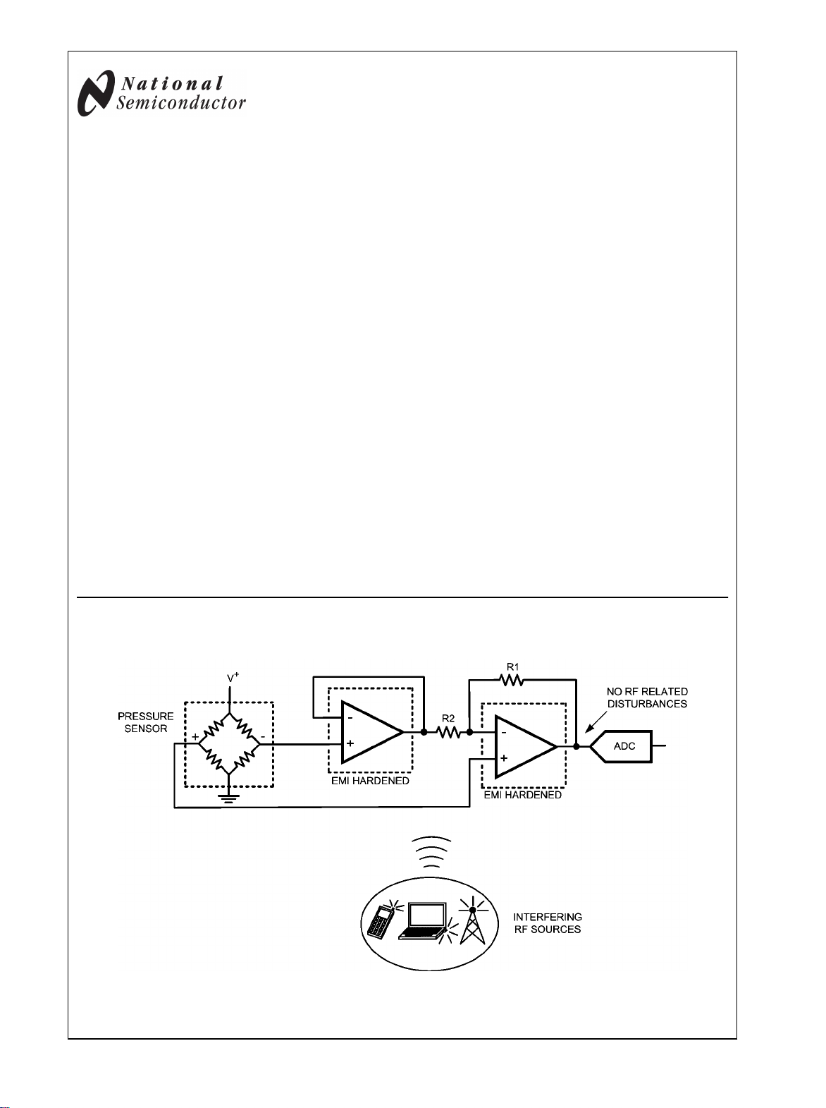
Typical Application
Features
Unless otherwise noted, typical values at TA = 25°C,
V
= 3.3V
SUPPLY
Supply voltage 2.7V to 5.5V
■
Supply current (per channel) 0.4 mA
■
Input offset voltage 1 mV max
■
Input bias current 0.1 pA
■
GBW 8 MHz
■
EMIRR at 1.8 GHz 87 dB
■
Input noise voltage at 1 kHz 11 nV/√Hz
■
Slew rate 4.5 V/µs
■
Output voltage swing Rail-to-Rail
■
Output current drive 30 mA
■
Operating ambient temperature range −40°C to 125°C
■
Applications
Photodiode preamp
■
Piezoelectric sensors
■
Portable/battery-powered electronic equipment
■
Filters/buffers
■
PDAs/phone accessories
■
Medical diagnosis equipment
■
Sensor Amplifiers Close to RF Sources
20202101
© 2007 National Semiconductor Corporation 202021 www.national.com

Absolute Maximum Ratings (Note 1)
LMV851 Single/ LMV852 Dual/ LMV854 Quad
Symbol Parameter Conditions Min
(Note 6)
I
O
Output Short Circuit Current Sourcing, V
OUT
= VCM,
VIN = 100 mV
Sinking, V
OUT
= VCM,
VIN = −100 mV
I
S
Supply Current LMV851 0.42 0.50
25
20
28
20
Typ
(Note 5)
28
31
Max
(Note 6)
Units
mA
0.58
LMV852 0.79 0.90
1.06
mA
LMV854 1.54 1.67
1.99
SR Slew Rate (Note 7) AV = +1, V
OUT
= 1 VPP,
4.5
V/μs
10% to 90%
GBW Gain Bandwidth Product 8 MHz
Φ
m
e
n
Phase Margin 62
Input-Referred Voltage Noise f = 1 kHz 11
f = 10 kHz 10
i
n
R
OUT
C
IN
Input-Referred Current Noise f = 1 kHz 0.005
Closed Loop Output Impedance f = 6 MHz 400
Common-Mode Input Capacitance 11
Differential-Mode Input Capacitance 6
THD+N Total Harmonic Distortion + Noise f = 1 kHz, AV = 1, BW = >500 kHz 0.006
deg
nV/
pA/
Ω
pF
%
5V Electrical Characteristics (Note 4)
Unless otherwise specified, all limits are guaranteed for TA = 25°C, V+ = 5V, V− = 0V, VCM = V+/2, and RL = 10 kΩ to V+/2.
Boldface limits apply at the temperature extremes.
Symbol Parameter Conditions Min
(Note 6)
V
OS
TCV
Input Offset Voltage ±0.26
Input Offset Voltage Drift
OS
±0.4
(Note 10)
I
B
Input Bias Current
0.1 10
(Note 10)
I
OS
CMRR Common Mode Rejection Ratio
PSRR Power Supply Rejection Ratio
EMIRR EMI Rejection Ratio, IN+ and IN−
Input Offset Current 1
−0.2V ≤ V
≤ V+ −1.2V
CM
2.7V ≤ V+ ≤ 5.5V,
V
= 1V
OUT
V
= 100 mVP (−20 dBVP),
(Note 8)
RFpeak
f = 400 MHz
V
= 100 mVP (−20 dBVP),
RFpeak
f = 900 MHz
V
= 100 mVP (−20 dBVP),
RFpeak
f = 1800 MHz
V
= 100 mVP (−20 dBVP),
RFpeak
f = 2400 MHz
CMVR Input Common-Mode Voltage Range
CMRR ≥ 77 dB
77
76
75
74
64
76
84
89
−0.2 3.8
Typ
(Note 5)
(Note 9)
(Note 9)
94
(Note 9)
93
(Note 9)
Max
(Note 6)
±1
±1.2
±2
500
Units
mV
μV/°C
pA
pA
dB
dB
dB
V
3 www.national.com

Symbol Parameter Conditions Min
(Note 6)
A
VOL
Large Signal Voltage Gain
(Note 11)
RL = 2 kΩ,
V
= 0.15V to 2.5V,
OUT
V
= 4.85V to 2.5V
OUT
RL = 10 kΩ,
V
= 0.1V to 2.5V,
OUT
V
= 4.9V to 2.5V
OUT
V
O
Output Swing High,
RL = 2 kΩ to V+/2
(measured from V+)
RL = 10 kΩ to V+/2
Output Swing Low,
RL = 2 kΩ to V+/2
(measured from V−)
RL = 10 kΩ to V+/2
I
O
Output Short Circuit Current Sourcing, V
OUT
= VCM,
VIN = 100 mV
Sinking, V
OUT
= VCM,
VIN = −100 mV
I
S
Supply Current LMV851 0.43 0.52
LMV852 0.82 0.93
LMV854 1.59 1.73
SR Slew Rate (Note 7) AV = +1, V
= 2 VPP,
OUT
10% to 90%
Typ
105
(Note 5)
118
(Note 6)
102
105
120
102
34 39
7 11
31 38
7 12
60
65
48
58
62
44
4.5
Max
47
13
50
15
0.60
1.09
2.05
Units
dB
mV
mV
mA
mA
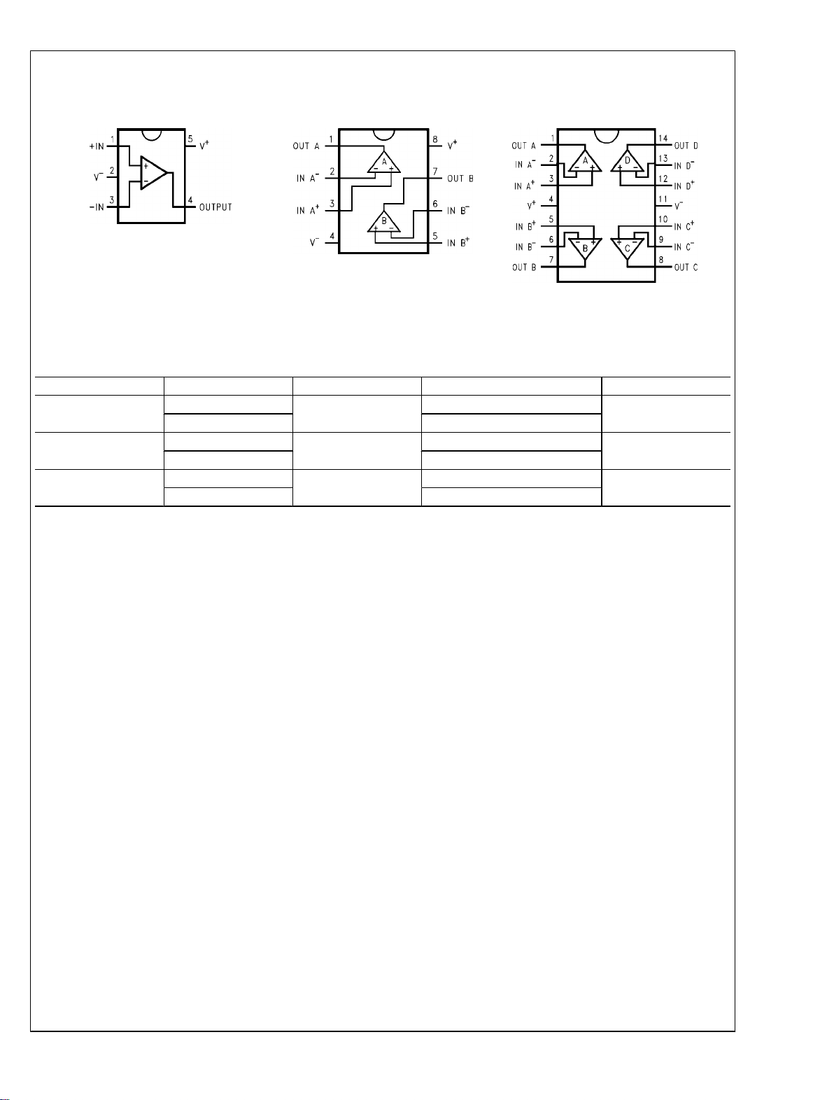
Connection Diagrams
LMV851 Single/ LMV852 Dual/ LMV854 Quad
5-Pin SC70
Top View
20202102
8-Pin MSOP
Top View
14-Pin TSSOP
20202103
Top View
Ordering Information
Package Part Number Package Marking Transport Media NSC Drawing
5-Pin SC70
8-Pin MSOP
14-Pin TSSOP
LMV851MG
LMV851MGX 3k Units Tape and Reel
LMV852MM
LMV852MMX 3.5k Units Tape and Reel
LMV854MT
LMV854MTX 2.5k Units Tape and Reel
A98
AB5A
LMV854MT
1k Units Tape and Reel
1k Units Tape and Reel
94 Units/Rail
20202104
MAA05A
MUA08A
MTC14
5 www.national.com
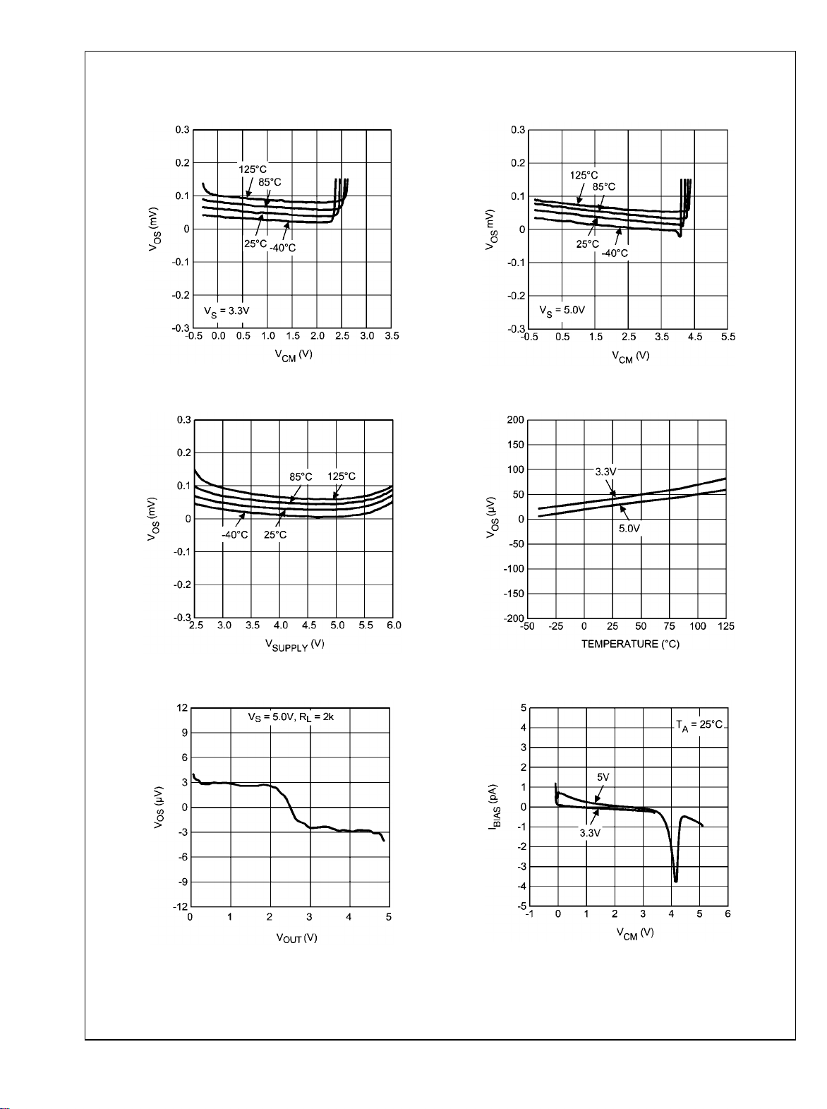
Typical Performance Characteristics At T
= 25°C, RL = 10 kΩ, VS = 3.3V, unless otherwise specified.
A
VOS vs. VCM at 3.3V
LMV851 Single/ LMV852 Dual/ LMV854 Quad
20202110
VOS vs. Supply Voltage
VOS vs. VCM at 5.0V
20202111
VOS vs. Temperature
20202112
VOS vs. V
www.national.com 6
OUT
20202114
20202113
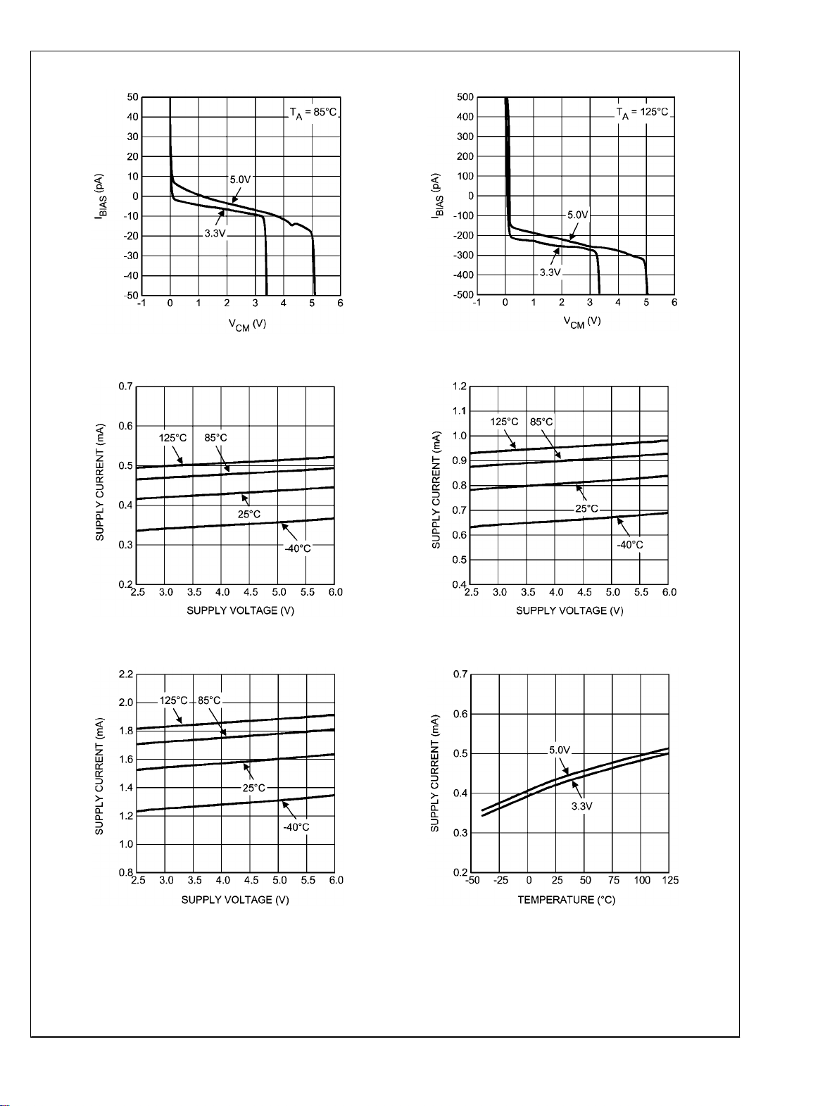
Input Bias Current vs. VCM at 25°C
20202115
LMV851 Single/ LMV852 Dual/ LMV854 Quad
Input Bias Current vs. VCM at 85°C
20202116
Supply Current vs. Supply Voltage Single LMV851
Input Bias Current vs. VCM at 125°C
20202117
Supply Current vs. Supply Voltage Dual LMV852
20202118
Supply Current vs. Supply Voltage Quad LMV854
20202120
20202119
Supply Current vs. Temperature Single LMV851
20202121
7 www.national.com

Supply Current vs. Temperature Dual LMV852
Supply Current vs. Temperature Quad LMV854
20202122
LMV851 Single/ LMV852 Dual/ LMV854 Quad
Sinking Current vs. Supply Voltage
20202124
Output Swing High vs. Supply Voltage RL = 2 kΩ
20202123
Sourcing Current vs. Supply Voltage
20202125
Output Swing High vs. Supply Voltage RL = 10 kΩ
20202126
www.national.com 8
20202127

LMV851 Single/ LMV852 Dual/ LMV854 Quad
Output Swing Low vs. Supply Voltage RL = 2 kΩ
20202128
Output Voltage Swing vs. Load Current at 3.3V
Output Swing Low vs. Supply Voltage RL = 10 kΩ
20202129
Output Voltage Swing vs. Load Current at 5.0V
20202155
Open Loop Frequency Response vs. Temperature
20202131
20202156
Open Loop Frequency Response vs. Load Conditions
20202132
9 www.national.com

Phase Margin vs. Capacitive Load
PSRR vs. Frequency
CMRR vs. Frequency
20202133
20202136
20202135

LMV851 Single/ LMV852 Dual/ LMV854 Quad
Small Signal Step Response with Gain = 1
20202140
Slew Rate vs. Supply Voltage
Small Signal Step Response with Gain = 10
20202141
Overshoot vs. Capacitive Load
Input Voltage Noise vs. Frequency
20202142
20202144
20202143
THD+N vs. Frequency
20202145
11 www.national.com

THD+N vs. Amplitude
R
vs. Frequency
OUT
LMV851 Single/ LMV852 Dual/ LMV854 Quad
EMIRR IN+ vs. Power at 400 MHz
EMIRR IN+ vs. Power at 1800 MHz
20202146
20202149
20202148
EMIRR IN+ vs. Power at 900 MHz
20202150
EMIRR IN+ vs. Power at 2400 MHz
20202151
www.national.com 12
20202152

LMV851 Single/ LMV852 Dual/ LMV854 Quad
EMIRR IN+ vs. Frequency at 3.3V
20202153
EMIRR IN+ vs. Frequency at 5.0V
20202154
13 www.national.com

Application Information
INTRODUCTION
The LMV851/LMV852/LMV854 are operational amplifiers
with very good specifications, such as low offset, low noise
and a rail-to-rail output. These specifications make the
LMV851/LMV852/LMV854 great choices to use in areas such
as medical and instrumentation. The low supply current is
perfect for battery powered equipment. The small packages,
SC-70 package for the LMV851, the MSOP package for the
dual LMV852 and the TSSOP package for the quad LMV854,
make any of these parts a perfect choice for portable electronics. Additionally, the EMI hardening makes the LMV851/
LMV852 or LMV854 a must for almost all op amp applications.
Most applications are exposed to Radio Frequency (RF) signals such as the signals transmitted by mobile phones or
wireless computer peripherals. The LMV851/LMV852/
LMV854 will effectively reduce disturbances caused by RF
signals to a level that will be hardly noticeable. This again
reduces the need for additional filtering and shielding. Using
this EMI resistant series of op amps will thus reduce the num-
LMV851 Single/ LMV852 Dual/ LMV854 Quad
ber of components and space needed for applications that are
affected by EMI, and will help applications, not yet identified
as possible EMI sensitive, to be more robust for EMI.
INPUT CHARACTERISTICS
The input common mode voltage range of the LMV851/
LMV852/LMV854 includes ground, and can even sense well
below ground. The CMRR level does not degrade for input
levels up to 1.2V below the supply voltage. For a supply voltage of 5V, the maximum voltage that should be applied to the
input for best CMRR performance is thus 3.8V.
When not configured as unity gain, this input limitation will
usually not degrade the effective signal range. The output is
rail-to-rail and therefore will introduce no limitations to the
signal range.
The typical offset is only 0.26 mV, and the TCVOS is
0.4 μV/°C, specifications close to precision op amps.
CMRR MEASUREMENT
The CMRR measurement results may need some clarification. This is because different setups are used to measure the
AC CMRR and the DC CMRR.
The DC CMRR is derived from ΔVOS versus ΔVCM. This value
is stated in the tables, and is tested during production testing.
The AC CMRR is measured with the test circuit shown in
Figure 1.
20202164
FIGURE 1. AC CMRR Measurement Setup
The configuration is largely the usually applied balanced configuration. With potentiometer P1, the balance can be tuned
to compensate for the DC offset in the DUT. The main difference is the addition of the buffer. This buffer prevents the
open-loop output impedance of the DUT from affecting the
balance of the feedback network. Now the closed-loop output
impedance of the buffer is a part of the balance. But as the
closed-loop output impedance is much lower, and by careful
selection of the buffer also has a larger bandwidth, the total
effect is that the CMRR of the DUT can be measured much
more accurately. The differences are apparent in the larger
measured bandwidth of the AC CMRR.
One artifact from this test circuit is that the low frequency CMRR results appear higher than expected. This is because in
the AC CMRR test circuit the potentiometer is used to compensate for the DC mismatches. So, mainly AC mismatch is
all that remains. Therefore, the obtained DC CMRR from this
AC CMRR test circuit tends to be higher than the actual DC
CMRR based on DC measurements.
The CMRR curve in Figure 2 shows a combination of the AC
CMRR and the DC CMRR.
www.national.com 14
20202136
FIGURE 2. CMRR Curve

LMV851 Single/ LMV852 Dual/ LMV854 Quad
OUTPUT CHARACTERISTICS
As already mentioned the output is rail to rail. When loading
the output with a 10 kΩ resistor the maximum swing of the
output is typically 7 mV from the positive and negative rail
The LMV851/LMV852/LMV854 can be connected as non-inverting unity gain amplifiers. This configuration is the most
sensitive to capacitive loading. The combination of a capacitive load placed at the output of an amplifier along with the
amplifier’s output impedance creates a phase lag, which reduces the phase margin of the amplifier. If the phase margin
is significantly reduced, the response will be under damped
which causes peaking in the transfer and, when there is too
much peaking, the op amp might start oscillating. The
LMV851/LMV852/LMV854 can directly drive capacitive loads
up to 200 pF without any stability issues. In order to drive
heavier capacitive loads, an isolation resistor, R
used, as shown in Figure 3. By using this isolation resistor,
, should be
ISO
the capacitive load is isolated from the amplifier’s output, and
hence, the pole caused by CL is no longer in the feedback
loop. The larger the value of R
fier will be. If the value of R
back loop will be stable, independent of the value of CL.
However, larger values of R
and reduced output current drive.
, the more stable the ampli-
ISO
is sufficiently large, the feed-
ISO
result in reduced output swing
ISO
Clearly the output voltage varies in the rhythm of the on-off
keying of the RF carrier.
20202165
FIGURE 4. Offset Voltage Variation Due to an Interfering
RF Signal
EMIRR Definition
To identify EMI hardened op amps, a parameter is needed
that quantitatively describes the EMI performance of op
amps. A quantitative measure enables the comparison and
the ranking of op amps on their EMI robustness. Therefore
the EMI Rejection Ratio (EMIRR) is introduced. This parameter describes the resulting input-referred offset voltage shift
of an op amp as a result of an applied RF carrier (interference)
with a certain frequency and level. The definition of EMIRR is
given by:
20202163
FIGURE 3. Isolating Capacitive Load
EMIRR
With the increase of RF transmitting devices in the world, the
electromagnetic interference (EMI) between those devices
and other equipment becomes a bigger challenge. The
LMV851/LMV852/LMV854 are EMI hardened op amps which
are specifically designed to overcome electromagnetic interference. Along with EMI hardened op amps, the EMIRR parameter is introduced to unambiguously specify the EMI
performance of an op amp. This section presents an overview
of EMIRR. A detailed description on this specification for EMI
hardened op amps can be found in Application Note AN-1698.
The dimensions of an op amp IC are relatively small compared to the wavelength of the disturbing RF signals. As a
result the op amp itself will hardly receive any disturbances.
The RF signals interfering with the op amp are dominantly
received by the PCB and wiring connected to the op amp. As
a result the RF signals on the pins of the op amp can be represented by voltages and currents. This representation significantly simplifies the unambiguous measurement and
specification of the EMI performance of an op amp.
RF signals interfere with op amps via the non-linearity of the
op amp circuitry. This non-linearity results in the detection of
the so called out-of-band signals. The obtained effect is that
the amplitude modulation of the out-of-band signal is downconverted into the base band. This base band can easily
overlap with the band of the op amp circuit. As an example
Figure 4 depicts a typical output signal of a unity-gain connected op amp in the presence of an interfering RF signal.
In which V
lated RF signal (V) and ΔVOS is the resulting input-referred
is the amplitude of the applied un-modu-
RF_PEAK
offset voltage shift (V). The offset voltage depends quadratically on the applied RF level, and therefore, the RF level at
which the EMIRR is determined should be specified. The
standard level for the RF signal is 100 mVP. Application Note
AN-1698 addresses the conversion of an EMIRR measured
for an other signal level than 100 mVP. The interpretation of
the EMIRR parameter is straightforward. When two op amps
have an EMIRR which differ by 20 dB, the resulting error signals when used in identical configurations, differs by 20 dB as
well. So, the higher the EMIRR, the more robust the op amp.
Coupling an RF Signal to the IN+ Pin
Each of the op amp pins can be tested separately on EMIRR.
In this section the measurements on the IN+ pin (which, based
on symmetry considerations, also apply to the IN− pin) are
discussed. In Application Note AN-1698 the other pins of the
op amp are treated as well. For testing the IN+ pin the op amp
is connected in the unity gain configuration. Applying the RF
signal is straightforward as it can be connected directly to the
IN+ pin. As a result the RF signal path has a minimum of components that might affect the RF signal level at the pin. The
circuit diagram is shown in Figure 5. The PCB trace from
RFIN to the IN+ pin should be a 50Ω stripline in order to match
the RF impedance of the cabling and the RF generator. On
the PCB a 50Ω termination is used. This 50Ω resistor is also
used to set the bias level of the IN+ pin to ground level. For
determining the EMIRR, two measurements are needed: one
is measuring the DC output level when the RF signal is off;
and the other is measuring the DC output level when the RF
signal is switched on. The difference of the two DC levels is
the output voltage shift as a result of the RF signal. As the op
amp is in the unity gain configuration, the input referred offset
15 www.national.com

voltage shift corresponds one-to-one to the measured output
voltage shift.
LMV851 Single/ LMV852 Dual/ LMV854 Quad
20202167
FIGURE 5. Circuit for Coupling the RF Signal to IN
Cell Phone Call
The effect of electromagnetic interference is demonstrated in
a setup where a cell phone interferes with a pressure sensor
application (Figure 7). This application needs two op amps
and therefore a dual op amp is used. The experiment is performed on two different dual op amps: a typical standard op
amp and the LMV852, EMI hardened dual op amp. The op
amps are placed in a single supply configuration. The cell
phone is placed on a fixed position a couple of centimeters
from the op amps.
When the cell phone is called, the PCB and wiring connected
to the op amps receive the RF signal. Subsequently, the op
amps detect the RF voltages and currents that end up at their
pins. The resulting effect on the output of the second op amp
is shown in Figure 6.
DECOUPLING AND LAYOUT
Care must be given when creating a board layout for the op
amp. For decoupling the supply lines it is suggested that
10 nF capacitors be placed as close as possible to the op
amp. For single supply, place a capacitor between V+ and
V−. For dual supplies, place one capacitor between V+ and
the board ground, and a second capacitor between ground
and V−. Even with the LMV851/LMV852/LMV854 inherent
hardening against EMI, it is still recommended to keep the
input traces short and as far as possible from RF sources.
Then the RF signals entering the chip are as low as possible,
and the remaining EMI can be, almost, completely eliminated
in the chip by the EMI reducing features of the LMV851/
LMV852/LMV854.
PRESSURE SENSOR APPLICATION
The LMV851/LMV852/LMV854 can be used for pressure sensor applications. Because of their low power the LMV851/
LMV852/LMV854 are ideal for portable applications, such as
blood pressure measurement devices, or portable barometers. This example describes a universal pressure sensor that
can be used as a starting point for different types of sensors
+
and applications.
Pressure Sensor Characteristics
The pressure sensor used in this example functions as a
Wheatstone bridge. The value of the resistors in the bridge
change when pressure is applied to the sensor. This change
of the resistor values will result in a differential output voltage,
depending on the sensitivity of the sensor and the applied
pressure. The difference between the output at full scale
pressure and the output at zero pressure is defined as the
span of the pressure sensor. A typical value for the span is
100 mV. A typical value for the resistors in the bridge is
5 kΩ. Loading of the resistor bridge could result in incorrect
output voltages of the sensor. Therefore the selection of the
circuit configuration, which connects to the sensor, should
take into account a minimum loading of the sensor.
Pressure Sensor Example
The configuration shown in Figure 7 is simple, and is very
useful for the read out of pressure sensors. With two op amps
in this application, the dual LMV852 fits very well.
The op amp configured as a buffer and connected at the negative output of the pressure sensor prevents the loading of the
bridge by resistor R2. The buffer also prevents the resistors
of the sensor from affecting the gain of the following gain
stage. Given the differential output voltage VS of the pressure
sensor, the output signal of this op amp configuration, V
equals:
OUT
,
20202168
FIGURE 6. Comparing EMI Robustness
The difference between the two types of dual op amps is
clearly visible. The typical standard dual op amp has an output
shift (disturbed signal) larger than 1V as a result of the RF
signal transmitted by the cell phone. The LMV852, EMI hardened op amp does not show any significant disturbances.
www.national.com 16
To align the pressure range with the full range of an ADC, the
power supply voltage and the span of the pressure sensor are
needed. For this example a power supply of 5V is used and
the span of the sensor is 100 mV.
When a 100Ω resistor is used for R2, and a 2.4 kΩ resistor is
used for R1, the maximum voltage at the output is 4.95V and
the minimum voltage is 0.05V. This signal is covering almost
the full input range of the ADC. Further processing can take
place in the microprocessor following the ADC.

FIGURE 7. Pressure Sensor Application
THERMOCOUPLE AMPLIFIER
The following circuit is a typical example for a thermocouple
amplifier application using an LMV851/LMV852, or LMV854.
A thermocouple converts a temperature into a voltage. This
signal is then amplified by the LMV851/LMV852, or LMV854.
An ADC can convert the amplified signal to a digital signal.
For further processing the digital signal can be processed by
a microprocessor and used to display or log the temperature.
The temperature data can for instance be used in a fabrication
process.
LMV851 Single/ LMV852 Dual/ LMV854 Quad
20202160
Characteristics of a Thermocouple
A thermocouple is a junction of two different metals. These
metals produce a small voltage that increases with temperature.
The thermocouple used in this application is a K-type thermocouple. A K-type thermocouple is a junction between Nickel-Chromium and Nickel-Aluminum. This is one of the most
commonly used thermocouples. There are several reasons
for using the K-type thermocouple, these include: temperature range, the linearity, the sensitivity, and the cost.
A K-type thermocouple has a wide temperature range. The
range of this thermocouple is from approximately −200°C to
approximately 1200°C, as can be seen in Figure 8. This cov-
ers the generally used temperature ranges.
Over the main part of the temperature range the output voltage depends linearly on the temperature. This is important for
easily converting the measured signal levels to a temperature
reading.
The K-type thermocouple has good sensitivity when compared to many other types; the sensitivity is about 41 uV/°C.
Lower sensitivity requires more gain and makes the application more sensitive to noise.
In addition, a K-type thermocouple is not expensive, many
other thermocouples consist of more expensive materials or
are more difficult to produce.
20202162
FIGURE 8. K-Type Thermocouple Response
Thermocouple Example
For this example, suppose the range of interest is 0°C to
500°C, and the resolution needed is 0.5°C. The power supply
for both the LMV851/LMV852, or LMV854 and the ADC is
3.3V.
The temperature range of 0°C to 500°C results in a voltage
range from 0 mV to 20.6 mV produced by the thermocouple.
This is indicated in Figure 8 by the dotted lines.
To obtain the highest resolution, the full ADC range of 0 to
3.3V is used. The gain needed for the full range can be calculated as follows:
AV = 3.3V / 0.0206V = 160
If RG is 2 kΩ, then the value for RF can be calculated for a gain
of 160. Since AV = RF / RG, RF can be calculated as follows:
RF = AV x RG = 160 x 2 kΩ = 320 kΩ
To get a resolution of 0.5°C, the LSB of the ADC should be
smaller then 0.5°C / 500°C = 1/1000. A 10-bit ADC would be
sufficient as this gives 1024 steps. A 10-bit ADC such as the
two channel 10-bit ADC102S021 can be used.
17 www.national.com

Unwanted Thermocouple Effect
At the point where the thermocouple wires are connected to
the circuit, usually copper wires or traces, an unwanted thermocouple effect will occur.
At this connection, this could be the connector on a PCB, the
thermocouple wiring forms a second thermocouple with the
connector. This second thermocouple disturbs the measurements from the intended thermocouple.
Using an isothermal block as a reference enables correction
for this unwanted thermocouple effect. An isothermal block is
a good heat conductor. This means that the two thermocouple
LMV851 Single/ LMV852 Dual/ LMV854 Quad
connections both have the same temperature. The temperature of the isothermal block can be measured, and thereby
the temperature of the thermocouple connections. This is
usually called the cold junction reference temperature.
In the example, an LM35 is used to measure this temperature.
This semiconductor temperature sensor can accurately measure temperatures from −55°C to 150°C.
The two channel ADC in this example also converts the signal
from the LM35 to a digital signal. Now the microprocessor can
compensate the amplified thermocouple signal, for the unwanted thermocouple effect.
20202161
FIGURE 9. Thermocouple Read Out Circuit
www.national.com 18

Physical Dimensions inches (millimeters) unless otherwise noted
LMV851 Single/ LMV852 Dual/ LMV854 Quad
NS Package Number MAA05A
5-Pin SC70
NS Package Number MUA08A
8-Pin MSOP
19 www.national.com

LMV851 Single/ LMV852 Dual/ LMV854 Quad
NS Package Number MTC14
14-Pin TSSOP
www.national.com 20

Notes
LMV851 Single/ LMV852 Dual/ LMV854 Quad
21 www.national.com

Amplifiers
Notes
THE CONTENTS OF THIS DOCUMENT ARE PROVIDED IN CONNECTION WITH NATIONAL SEMICONDUCTOR CORPORATION
(“NATIONAL”) PRODUCTS. NATIONAL MAKES NO REPRESENTATIONS OR WARRANTIES WITH RESPECT TO THE ACCURACY
OR COMPLETENESS OF THE CONTENTS OF THIS PUBLICATION AND RESERVES THE RIGHT TO MAKE CHANGES TO
SPECIFICATIONS AND PRODUCT DESCRIPTIONS AT ANY TIME WITHOUT NOTICE. NO LICENSE, WHETHER EXPRESS,
IMPLIED, ARISING BY ESTOPPEL OR OTHERWISE, TO ANY INTELLECTUAL PROPERTY RIGHTS IS GRANTED BY THIS
DOCUMENT.
TESTING AND OTHER QUALITY CONTROLS ARE USED TO THE EXTENT NATIONAL DEEMS NECESSARY TO SUPPORT
NATIONAL’S PRODUCT WARRANTY. EXCEPT WHERE MANDATED BY GOVERNMENT REQUIREMENTS, TESTING OF ALL
PARAMETERS OF EACH PRODUCT IS NOT NECESSARILY PERFORMED. NATIONAL ASSUMES NO LIABILITY FOR
APPLICATIONS ASSISTANCE OR BUYER PRODUCT DESIGN. BUYERS ARE RESPONSIBLE FOR THEIR PRODUCTS AND
APPLICATIONS USING NATIONAL COMPONENTS. PRIOR TO USING OR DISTRIBUTING ANY PRODUCTS THAT INCLUDE
NATIONAL COMPONENTS, BUYERS SHOULD PROVIDE ADEQUATE DESIGN, TESTING AND OPERATING SAFEGUARDS.
EXCEPT AS PROVIDED IN NATIONAL’S TERMS AND CONDITIONS OF SALE FOR SUCH PRODUCTS, NATIONAL ASSUMES NO
LIABILITY WHATSOEVER, AND NATIONAL DISCLAIMS ANY EXPRESS OR IMPLIED WARRANTY RELATING TO THE SALE
AND/OR USE OF NATIONAL PRODUCTS INCLUDING LIABILITY OR WARRANTIES RELATING TO FITNESS FOR A PARTICULAR
PURPOSE, MERCHANTABILITY, OR INFRINGEMENT OF ANY PATENT, COPYRIGHT OR OTHER INTELLECTUAL PROPERTY
RIGHT.
LIFE SUPPORT POLICY
NATIONAL’S PRODUCTS ARE NOT AUTHORIZED FOR USE AS CRITICAL COMPONENTS IN LIFE SUPPORT DEVICES OR
SYSTEMS WITHOUT THE EXPRESS PRIOR WRITTEN APPROVAL OF THE CHIEF EXECUTIVE OFFICER AND GENERAL
COUNSEL OF NATIONAL SEMICONDUCTOR CORPORATION. As used herein:
Life support devices or systems are devices which (a) are intended for surgical implant into the body, or (b) support or sustain life and
whose failure to perform when properly used in accordance with instructions for use provided in the labeling can be reasonably expected
to result in a significant injury to the user. A critical component is any component in a life support device or system whose failure to perform
can be reasonably expected to cause the failure of the life support device or system or to affect its safety or effectiveness.
National Semiconductor and the National Semiconductor logo are registered trademarks of National Semiconductor Corporation. All other
brand or product names may be trademarks or registered trademarks of their respective holders.
Copyright© 2007 National Semiconductor Corporation
For the most current product information visit us at www.national.com
National Semiconductor
Americas Customer
Support Center
Email:
new.feedback@nsc.com
Tel: 1-800-272-9959
LMV851 Single/ LMV852 Dual/ LMV854 Quad 8 MHz Low Power CMOS, EMI Hardened Operational
www.national.com
National Semiconductor Europe
Customer Support Center
Fax: +49 (0) 180-530-85-86
Email: europe.support@nsc.com
Deutsch Tel: +49 (0) 69 9508 6208
English Tel: +49 (0) 870 24 0 2171
Français Tel: +33 (0) 1 41 91 8790
National Semiconductor Asia
Pacific Customer Support Center
Email: ap.support@nsc.com
National Semiconductor Japan
Customer Support Center
Fax: 81-3-5639-7507
Email: jpn.feedback@nsc.com
Tel: 81-3-5639-7560
 Loading...