

National Semiconductor LMV831 Technical data
October 6, 2008
LMV831 Single/ LMV832 Dual/ LMV834 Quad
3.3 MHz Low Power CMOS, EMI Hardened Operational
Amplifiers
LMV831 Single/ LMV832 Dual/ LMV834 Quad 3.3 MHz Low Power CMOS, EMI Hardened
Operational Amplifiers
General Description
National’s LMV831, LMV832, and LMV834 are CMOS input,
low power op amp IC's, providing a low input bias current, a
wide temperature range of −40°C to 125°C and exceptional
performance making them robust general purpose parts. Additionally, the LMV831/LMV832/LMV834 are EMI hardened
to minimize any interference so they are ideal for EMI sensitive applications.
The unity gain stable LMV831/LMV832/LMV834 feature
3.3 MHz of bandwidth while consuming only 0.24 mA of current per channel. These parts also maintain stability for capacitive loads as large as 200 pF. The LMV831/LMV832/
LMV834 provide superior performance and economy in terms
of power and space usage.
This family of parts has a maximum input offset voltage of
1 mV, a rail-to-rail output stage and an input common-mode
voltage range that includes ground. Over an operating range
from 2.7V to 5.5V the LMV831/LMV832/LMV834 provide a
PSRR of 93 dB, and a CMRR of 91 dB. The LMV831 is offered
in the space saving 5-Pin SC70 package, the LMV832 in the
8-Pin MSOP and the LMV834 is offered in the 14-Pin TSSOP
package.
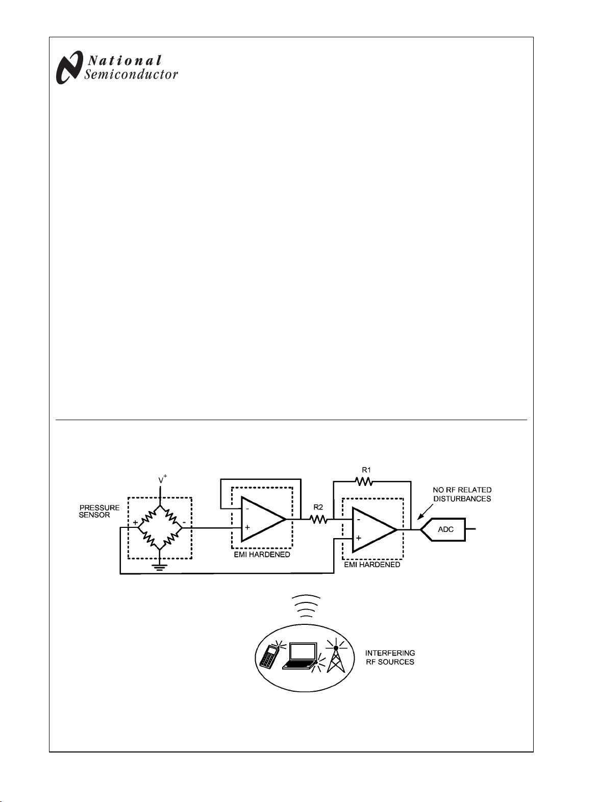
Typical Application
EMI Hardened Sensor Application
Features
Unless otherwise noted, typical values at TA= 25°C,
V+ = 3.3V
Supply voltage 2.7V to 5.5V
■
Supply current (per channel) 240 µA
■
Input offset voltage 1 mV max
■
Input bias current 0.1 pA
■
GBW 3.3 MHz
■
EMIRR at 1.8 GHz 120 dB
■
Input noise voltage at 1 kHz 12 nV/√Hz
■
Slew rate 2 V/µs
■
Output voltage swing Rail-to-Rail
■
Output current drive 30 mA
■
Operating ambient temperature range −40°C to 125°C
■
Applications
Photodiode preamp
■
Piezoelectric sensors
■
Portable/battery-powered electronic equipment
■
Filters/buffers
■
PDAs/phone accessories
■
30024101
© 2008 National Semiconductor Corporation 300241 www.national.com
Absolute Maximum Ratings (Note 1)
If Military/Aerospace specified devices are required,
please contact the National Semiconductor Sales Office/
Distributors for availability and specifications.
ESD Tolerance (Note 2)
Human Body Model 2 kV
Charge-Device Model 1 kV
Machine Model 200V
V
Differential
IN
Supply Voltage (VS = V+ – V−)
Voltage at Input/Output Pins V++0.4V,
± Supply Voltage
6V
V− −0.4V
Storage Temperature Range −65°C to 150°C
Junction Temperature (Note 3) 150°C
Soldering Information
Infrared or Convection (20 sec) 260°C
Operating Ratings (Note 1)
Temperature Range (Note 3) −40°C to 125°C
Supply Voltage (VS = V+ – V−)
Package Thermal Resistance (θJA (Note 3))
5-Pin SC-70 302°C/W
8-Pin MSOP 217°C/W
14-Pin TSSOP 135°C/W
3.3V Electrical Characteristics (Note 4)
Unless otherwise specified, all limits are guaranteed for at TA = 25°C, V+ = 3.3V, V− = 0V, VCM = V+/2, and RL =10 kΩ to V+/2.
Boldface limits apply at the temperature extremes.
Symbol Parameter Conditions Min
LMV831 Single/ LMV832 Dual/ LMV834 Quad
V
OS
TCV
I
B
I
OS
CMRR Common-Mode Rejection Ratio
PSRR Power Supply Rejection Ratio
EMIRR EMI Rejection Ratio, IN+ and IN-
CMVR Input Common-Mode Voltage Range
A
VOL
Input Offset Voltage
±0.25 ±1.00
(Note 9)
Input Offset Voltage Temperature Drift
OS
(Notes 9, 10)
LMV831,
LMV832
LMV834 ±0.5 ±1.7
Input Bias Current
0.1 10
(Note 10)
Input Offset Current 1
0.2V ≤ VCM ≤ V+ - 1.2V
(Note 9)
2.7V ≤ V+ ≤ 5.5V,
(Note 9)
(Note 8)
V
= 1V
OUT
V
=100 mVP (−20 dBP),
RF_PEAK
f = 400 MHz
V
=100 mVP (−20 dBP),
RF_PEAK
f = 900 MHz
V
=100 mVP (−20 dBP),
RF_PEAK
f = 1800 MHz
V
=100 mVP (−20 dBP),
RF_PEAK
f = 2400 MHz
CMRR ≥ 65 dB
Large Signal Voltage Gain
(Note 11)
RL = 2 kΩ,
V
= 0.15V to 1.65V,
OUT
V
= 3.15V to 1.65V
OUT
RL = 10 kΩ,
V
= 0.1V to 1.65V,
OUT
V
= 3.2V to 1.65V
OUT
LMV831,
LMV832
LMV834 102
LMV831,
LMV832
LMV834 104
(Note 6)
±0.5 ±1.5
76
75
76
75
80
90
110
120
−0.1 2.1
102
102
102
104
104
103
Typ
(Note 5)
91
93
121
121
126
123
(Note 6)
±1.23
2.7V to 5.5V
Max
500
Units
mV
μV/°C
pA
pA
dB
dB
dB
V
dB
www.national.com 2
LMV831 Single/ LMV832 Dual/ LMV834 Quad
Symbol Parameter Conditions Min
(Note 6)
V
OUT
Output Voltage Swing High
RL = 2 kΩ to V+/2
LMV831,
LMV832
29 36
Typ
(Note 5)
Max
(Note 6)
43
Units
LMV834 31 38
44
RL = 10 kΩ to V+/2
LMV831,
LMV832
LMV834 7 9
6 8
9
mV from
either rail
10
Output Voltage Swing Low
R = 2 kΩ to V+/2
25 34
43
RL = 10 kΩ to V+/2
5 8
10
I
OUT
I
S
Output Short Circuit Current Sourcing, V
VIN = 100 mV
OUT
= VCM,
LMV831,
LMV832
27
22
LMV834 24
28
28
19
Sinking, V
VIN = −100 mV
OUT
= VCM,
27
21
32
Supply Current LMV831 0.24 0.27
mA
0.30
LMV832 0.46 0.51
0.58
mA
LMV834 0.90 1.00
1.16
SR Slew Rate (Note 7) AV = +1, V
10% to 90%
OUT
= 1 VPP,
2
V/μs
GBW Gain Bandwidth Product 3.3 MHz
Φ
m
e
n
i
n
R
OUT
C
IN
Phase Margin 65
Input Referred Voltage Noise Density f = 1 kHz 12
Input Referred Current Noise Density f = 1 kHz 0.005
Closed Loop Output Impedance f = 2 MHz 500
Common-mode Input Capacitance 15
Differential-mode Input Capacitance 20
THD+N Total Harmonic Distortion + Noise
f = 10 kHz 10
f = 1 kHz, AV = 1, BW ≥ 500 kHz
0.02
deg
nV/
pA/
Ω
pF
%
5V Electrical Characteristics (Note 4)
Unless otherwise specified, all limits are guaranteed for at TA = 25°C, V+ = 5V, V− = 0V, VCM = V+/2, and RL = 10 kΩ to V+/2.
Boldface limits apply at the temperature extremes.
Symbol Parameter Conditions Min
(Note 6)
V
OS
Input Offset Voltage
±0.25 ±1.00
(Note 9)
TCV
Input Offset Voltage Temperature Drift
OS
(Notes 9, 10)
LMV831,
LMV832
LMV834 ±0.5 ±1.7
I
B
Input Bias Current
0.1 10
(Note 10)
I
OS
CMRR Common-Mode Rejection Ratio
Input Offset Current 1
(Note 9)
0V ≤ V
≤ V+ −1.2V
CM
3 www.national.com
±0.5 ±1.5
77
77
Typ
(Note 5)
93
Max
(Note 6)
±1.23
500
Units
mV
μV/°C
pA
pA
dB
Symbol Parameter Conditions Min
(Note 6)
PSRR Power Supply Rejection Ratio
(Note 9)
EMIRR EMI Rejection Ratio, IN+ and IN-
(Note 8)
2.7V ≤ V+ ≤ 5.5V,
V
= 1V
OUT
V
=100 mVP (−20 dBP),
RF_PEAK
f = 400 MHz
V
=100 mVP (−20 dBP),
RF_PEAK
76
75
80
90
Typ
(Note 5)
93
Max
(Note 6)
f = 900 MHz
V
=100 mVP (−20 dBP),
RF_PEAK
110
f = 1800 MHz
V
=100 mVP (−20 dBP),
RF_PEAK
120
f = 2400 MHz
CMVR Input Common-Mode Voltage Range
A
VOL
Large Signal Voltage Gain
(Note 11)
CMRR ≥ 65 dB
RL = 2 kΩ,
V
OUT
V
OUT
LMV831 Single/ LMV832 Dual/ LMV834 Quad
RL = 10 kΩ,
V
OUT
V
OUT
= 0.15V to 2.5V,
= 4.85V to 2.5V
= 0.1V to 2.5V,
= 4.9V to 2.5V
LMV831,
LMV832
LMV834 104
LMV831,
LMV832
LMV834 105
–0.1 3.8
107
127
106
127
104
107
130
107
127
104
V
OUT
Output Voltage Swing High
RL = 2 kΩ to V+/2
LMV831,
LMV832
32 42
49
LMV834 35 45
52
RL = 10 kΩ to V+/2
LMV831,
LMV832
6 9
10
LMV834 7 10
11
Output Voltage Swing Low
RL = 2 kΩ to V+/2
27 43
52
RL = 10 kΩ to V+/2
6 10
12
I
OUT
Output Short Circuit Current Sourcing V
VIN = 100 mV
OUT
= V
LMV831,
CM
LMV832
LMV834 57
59
49
66
63
45
Sinking V
VIN = −100 mV
OUT
= V
LMV831,
CM
LMV832
LMV834 53
50
41
64
63
41
I
S
Supply Current LMV831 0.25 0.27
0.31
LMV832 0.47 0.52
0.60
LMV834 0.92 1.02
1.18
SR Slew Rate (Note 7) AV = +1, V
OUT
= 2VPP,
2
10% to 90%
GBW Gain Bandwidth Product 3.3 MHz
Φ
m
e
n
Phase Margin 65
Input Referred Voltage Noise f = 1 kHz 12
f = 10 kHz 10
Units
dB
dB
V
dB
mV from
either rail
mA
mA
V/μs
deg
nV/
www.national.com 4
LMV831 Single/ LMV832 Dual/ LMV834 Quad
Symbol Parameter Conditions Min
(Note 6)
i
n
R
OUT
C
IN
Input Referred Current Noise f = 1 kHz 0.005
Closed Loop Output Impedance f = 2 MHz 500
Common-mode Input Capacitance 14
Typ
(Note 5)
Max
(Note 6)
pA/
Differential-mode Input Capacitance 20
THD+N Total Harmonic Distortion + Noise
Note 1: Absolute Maximum Ratings indicate limits beyond which damage to the device may occur. Operating Ratings indicate conditions for which the device is
intended to be functional, but specific performance is not guaranteed. For guaranteed specifications and the test conditions, see the Electrical Characteristics
Tables.
Note 2: Human Body Model, applicable std. MIL-STD-883, Method 3015.7. Machine Model, applicable std. JESD22-A115-A (ESD MM std. of JEDEC) FieldInduced Charge-Device Model, applicable std. JESD22-C101-C (ESD FICDM std. of JEDEC).
Note 3: The maximum power dissipation is a function of T
PD = (T
Note 4: Electrical Table values apply only for factory testing conditions at the temperature indicated. Factory testing conditions result in very limited self-heating
of the device such that TJ = TA. No guarantee of parametric performance is indicated in the electrical tables under conditions of internal self-heating where
TJ > TA.
Note 5: Typical values represent the most likely parametric norm as determined at the time of characterization. Actual typical values may vary over time and will
also depend on the application and configuration. The typical values are not tested and are not guaranteed on shipped production material.
Note 6: Limits are 100% production tested at 25°C. Limits over the operating temperature range are guaranteed through correlations using statistical quality
control (SQC) method.
Note 7: Number specified is the slower of positive and negative slew rates.
Note 8: The EMI Rejection Ratio is defined as EMIRR = 20log ( V
Note 9: The typical value is calculated by applying absolute value transform to the distribution, then taking the statistical average of the resulting distribution.
Note 10: This parameter is guaranteed by design and/or characterization and is not tested in production.
Note 11: The specified limits represent the lower of the measured values for each output range condition.
- TA)/ θJA . All numbers apply for packages soldered directly onto a PC board.
J(MAX)
f = 1 kHz, AV = 1, BW ≥ 500 kHz
, θJA, and TA. The maximum allowable power dissipation at any ambient temperature is
J(MAX)
/ΔVOS).
RF_PEAK
0.02
Units
Ω
pF
%
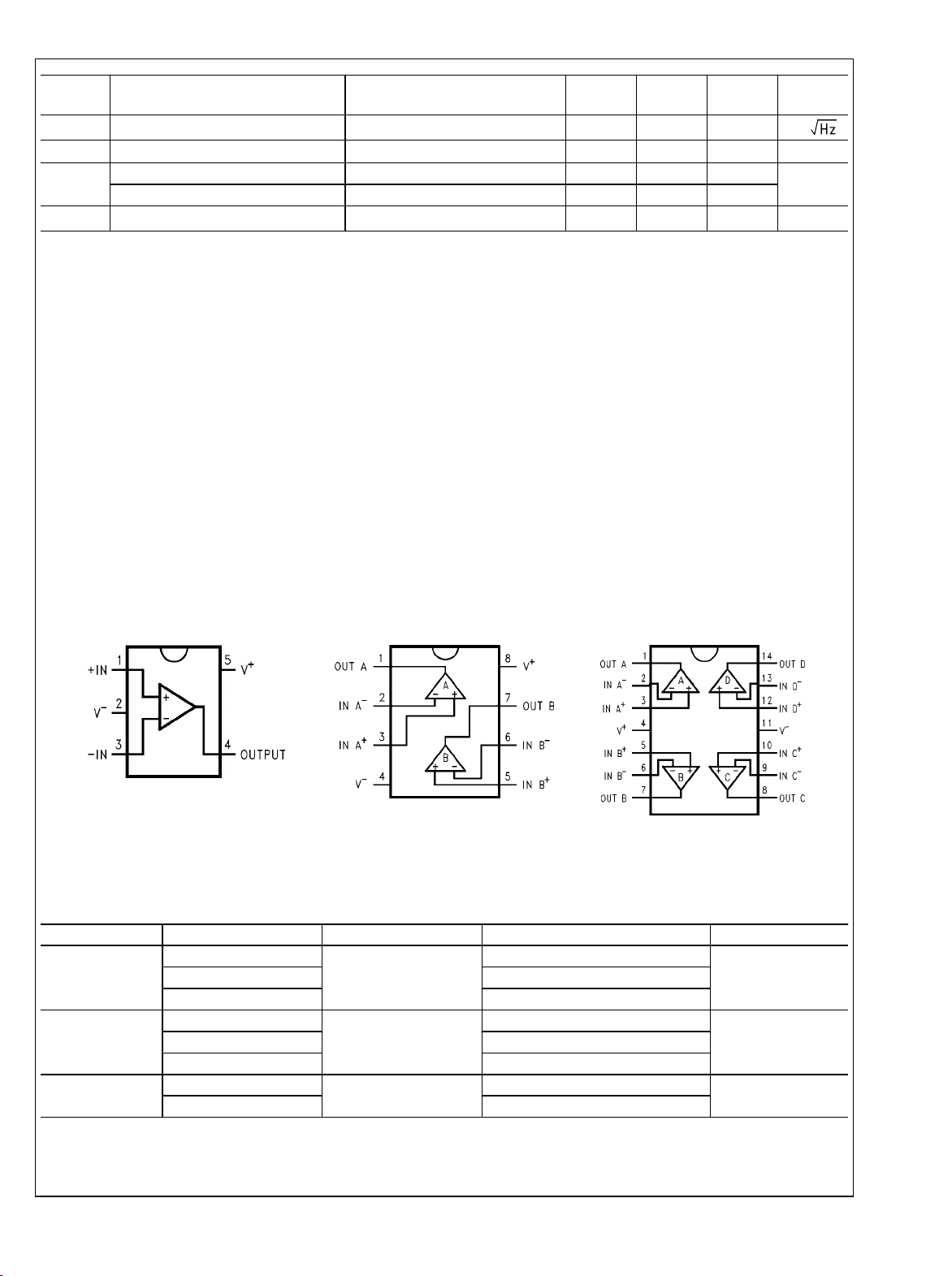
Connection Diagrams
5-Pin SC-70
Top View
30024102
8-Pin MSOP
Top View
30024103
14-Pin TSSOP
Top View
30024104
Ordering Information
Package Part Number Package Marking Transport Media NSC Drawing
5-Pin SC-70
8-Pin MSOP
14-Pin TSSOP
LMV831MG
AFA
LMV831MGX 3k Units Tape and Reel
LMV832MM
AU5A
LMV832MMX 3.5k Units Tape and Reel
LMV834MT
LMV834MTX 2.5k Units Tape and Reel
LMV834MT
1k Units Tape and Reel
1k Units Tape and Reel
94 Units/Rail
MAA05ALMV831MGE 250 Units Tape and Reel
MUA08ALMV832MME 250 Units Tape and Reel
MTC14
5 www.national.com
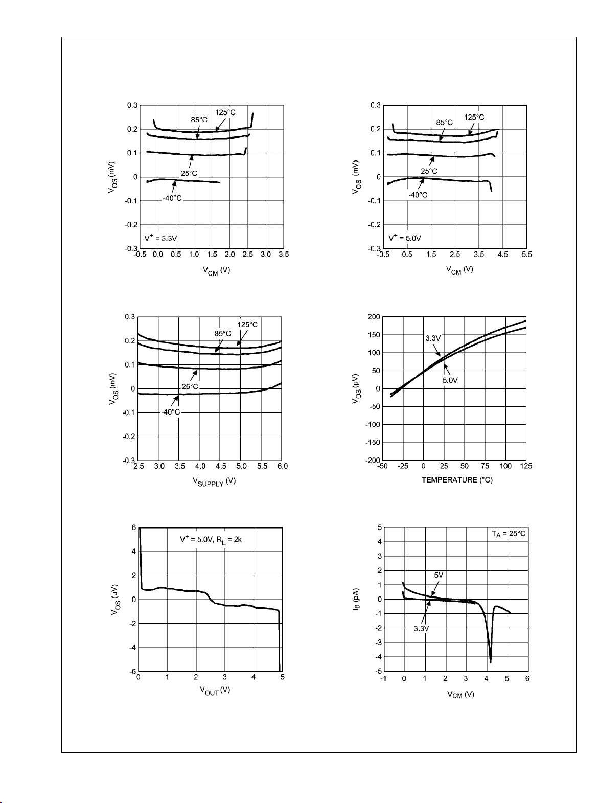
Typical Performance Characteristics At T
specified.
= 25°C, RL = 10 kΩ, V+ = 3.3V, V− = 0V, Unless otherwise
A
VOS vs. VCM at V+ = 3.3V
LMV831 Single/ LMV832 Dual/ LMV834 Quad
30024110
VOS vs. Supply Voltage
VOS vs. VCM at V+ = 5.0V
30024111
VOS vs. Temperature
30024112
VOS vs. V
www.national.com 6
OUT
30024114
30024113
Input Bias Current vs. VCM at 25°C
30024115
 Loading...