

National Semiconductor LMV771, LMV772, LMV774 General Description Manual
LMV771/LMV772/LMV774
Single/Dual/Quad, Low Offset, Low Noise, RRO
Operational Amplifiers
LMV771/LMV772/LMV774 Single/Dual/Quad, Low Offset, Low Noise, RRO Operational Amplifiers
April 2007
General Description
The LMV771/LMV772/LMV774 are Single, Dual, and Quad
low noise precision operational amplifiers intended for use in
a wide range of applications. Other important characteristics
of the family include: an extended operating temperature
range of −40°C to 125°C, the tiny SC70-5 package for the
LMV771, and low input bias current.
The extended temperature range of −40°C to 125°C allows
the LMV771/LMV772/LMV774 to accommodate a broad
range of applications. The LMV771 expands National
Semiconductor’s Silicon Dust™ amplifier portfolio offering enhancements in size, speed, and power savings. The LMV771/
LMV772/LMV774 are guaranteed to operate over the voltage
range of 2.7V to 5.0V and all have rail-to-rail output.
The LMV771/LMV772/LMV774 family is designed for precision, low noise, low voltage, and miniature systems. These
amplifiers provide rail-to-rail output swing into heavy loads.
The maximum input offset voltage for the LMV771 is 850 μV
at room temperature and the input common mode voltage
range includes ground.
The LMV771 is offered in the tiny SC70-5 package, LMV772
in the space saving MSOP-8 and SOIC-8, and the LMV774
in TSSOP-14.
Features
(Unless otherwise noted, typical values at VS = 2.7V)
Guaranteed 2.7V and 5V specifications
■
Maximum VOS (LMV771)
■
Voltage noise
■
f = 100Hz 12.5nV/
—
f = 10kHz 7.5nV/
—
Rail-to-Rail output swing
■
RL = 600Ω 100 mV from rail
—
RL = 2kΩ 50 mV from rail
—
Open loop gain with RL = 2kΩ 100 dB
■
V
■
CM
Supply current (per amplifier) 550 µA
■
Gain bandwidth product 3.5 MHz
■
Temperature range −40°C to 125°C
■
850μV (limit)
0 to V+ -0.9V
Applications
Transducer amplifier
■
Instrumentation amplifier
■
Precision current sensing
■
Data acquisition systems
■
Active filters and buffers
■
Sample and hold
■
Portable/battery powered electronics
■
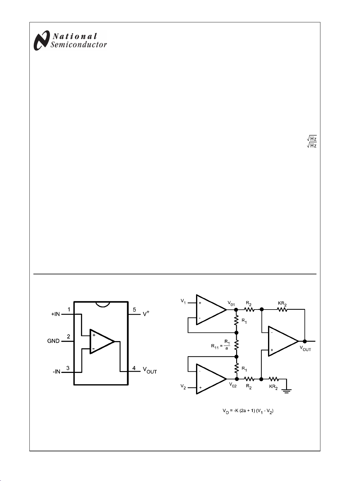
Connection Diagram
SC70-5
Top View
Silicon Dust™ is a trademark of National Semiconductor Corporation.
© 2007 National Semiconductor Corporation 200396 www.national.com
20039667
Instrumentation Amplifier
20039636
Absolute Maximum Ratings (Note 1)
If Military/Aerospace specified devices are required,
please contact the National Semiconductor Sales Office/
Distributors for availability and specifications.
ESD Tolerance (Note 2)
Machine Model 200V
Human Body Model 2000V
Differential Input Voltage ± Supply Voltage
Voltage at Input Pins (V+) + 0.3V, (V–) – 0.3V
LMV771/LMV772/LMV774
Current at Input Pins ±10 mA
Supply Voltage (V+–V −)
Output Short Circuit to V
Output Short Circuit to V
Mounting Temperture
+
−
5.75V
(Note 3)
(Note 4)
Infrared or Convection (20 sec) 235°C
Wave Soldering Lead Temp
(10 sec) 260°C
Storage Temperature Range −65°C to 150°C
Junction Temperature (Note 5) 150°C
Operating Ratings (Note 1)
Supply Voltage 2.7V to 5.5V
Temperature Range −40°C to 125°C
Thermal Resistance (θJA)
SC70-5 Package 440 °C/W
8-Pin MSOP 235°C/W
8-Pin SOIC 190°C/W
14-Pin TSSOP 155°C/W
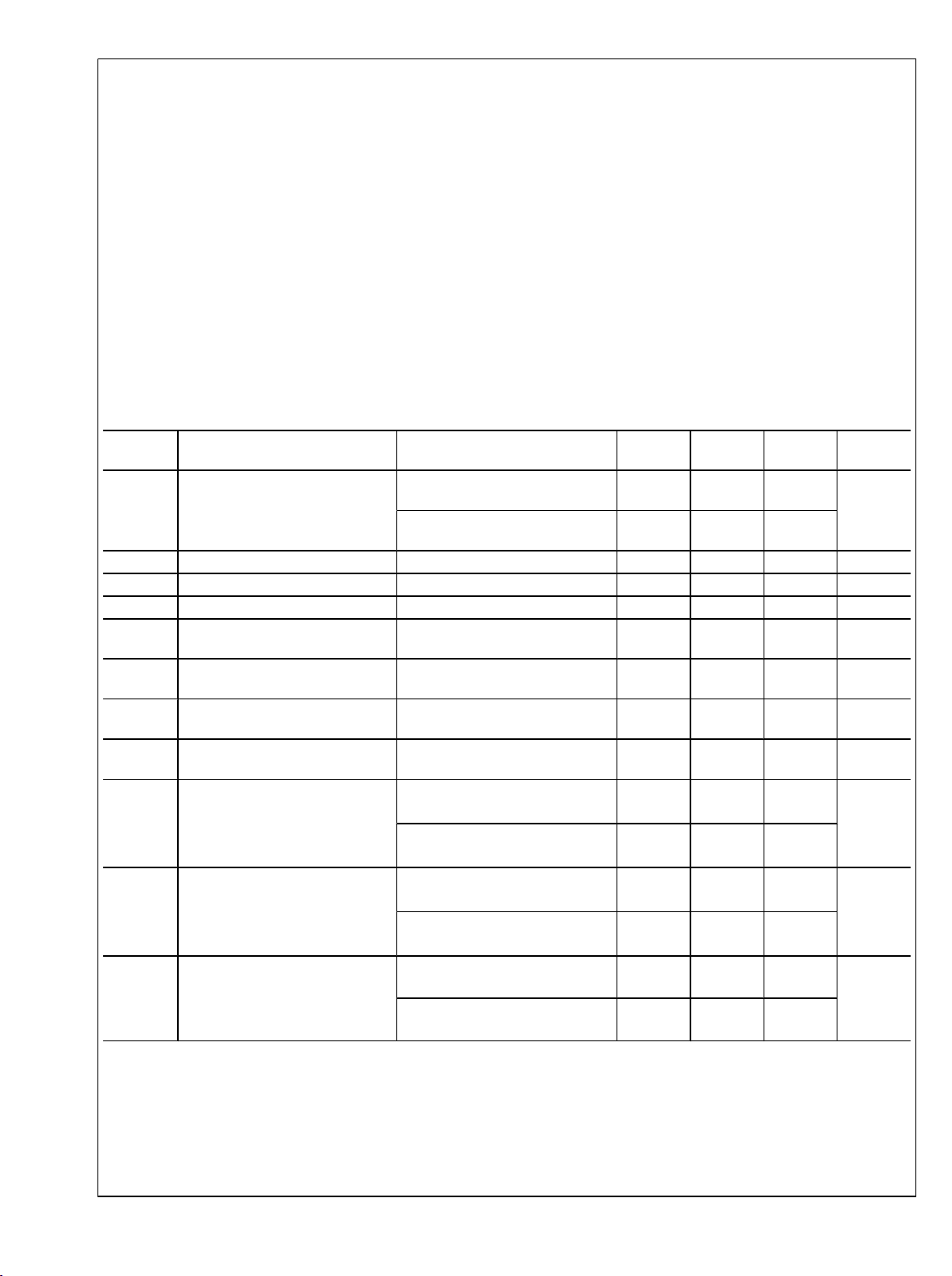
2.7V DC Electrical Characteristics (Note 13)
Unless otherwise specified, all limits are guaranteed for TA = 25°C. V+ = 2.7V, V − = 0V, VCM = V+/2, VO = V+/2 and
RL > 1MΩ. Boldface limits apply at the temperature extremes.
Symbol Parameter Condition Min
(Note 7)
V
OS
Input Offset Voltage LMV771 0.3 0.85
LMV772/LMV774 0.3 1.0
TCV
I
B
I
OS
I
S
CMRR Common Mode Rejection Ratio
Input Offset Voltage Average Drift −0.45 µV/°C
OS
Input Bias Current (Note 8) −0.1 100 pA
Input Offset Current (Note 8) 0.004 100 pA
Supply Current (Per Amplifier) 550 900
0.5 ≤ VCM ≤ 1.2V
74
72
PSSR Power Supply Rejection Ratio
2.7V ≤ V+ ≤ 5V
82
76
V
CM
Input Common-Mode Voltage
For CMRR ≥ 50dB
0 1.8 V
Range
A
V
V
O
I
O
Large Signal Voltage Gain
(Note 9)
RL = 600Ω to 1.35V,
VO = 0.2V to 2.5V, (Note 10)
RL = 2kΩ to 1.35V,
VO = 0.2V to 2.5V, (Note 11)
Output Swing
RL = 600Ω to 1.35V
VIN = ± 100mV, (Note 10)
RL = 2kΩ to 1.35V
VIN = ± 100mV, (Note 11)
Output Short Circuit Current Sourcing, VO = 0V
VIN = 100mV
Sinking, VO = 2.7V
VIN = −100mV
92
80
98
86
0.11
0.14
0.05
0.06
18
11
18
11
Typ
(Note 6)
80
90 dB
100
100
0.084 to
2.62
0.026 to
2.68
24
22
Max
(Note 7)
1.0
1.2
910
2.59
2.56
2.65
2.64
Units
mV
µA
dB
dB
V
mA
www.national.com 2
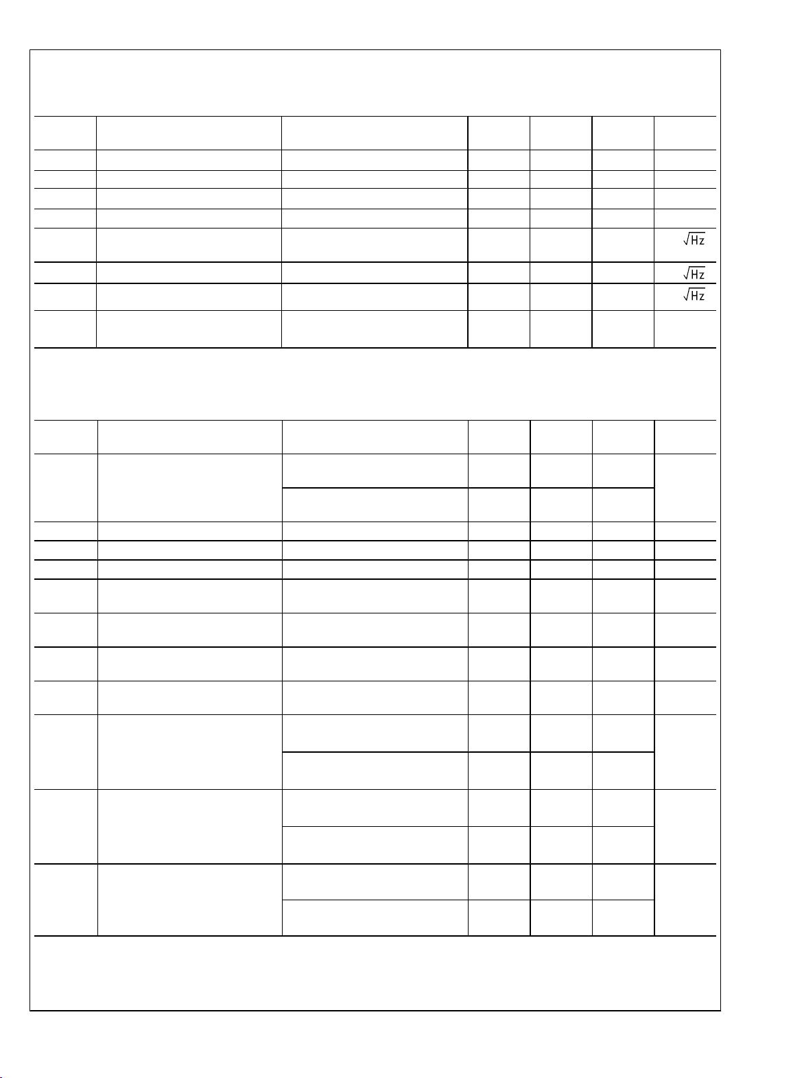
2.7V AC Electrical Characteristics (Note 13)
Unless otherwise specified, all limits are guaranteed for TA = 25°C. V+ = 5.0V, V − = 0V, VCM = V+/2, VO = V+/2 and RL > 1MΩ.
Boldface limits apply at the temperature extremes.
Symbol Parameter Conditions Min
(Note 7)
SR Slew Rate (Note 12)
AV = +1, RL = 10 kΩ
1.4 V/µs
GBW Gain-Bandwidth Product 3.5 MHz
Φ
m
G
m
e
n
Phase Margin 79 Deg
Gain Margin −15 dB
Input-Referred Voltage Noise
f = 10kHz 7.5
(Flatband)
e
n
i
n
Input-Referred Voltage Noise (l/f) f = 100Hz 12.5
Input-Referred Current Noise f = 1kHz 0.001
Typ
(Note 6)
Max
(Note 7)
Units
nV/
nV/
pA/
LMV771/LMV772/LMV774
THD Total Harmonic Distortion f = 1kHz, AV = +1
RL = 600Ω, VIN = 1 V
PP
0.007 %
5.0V DC Electrical Characteristics (Note 13)
Unless otherwise specified, all limits are guaranteed for TA = 25°C. V+ = 5.0V, V − = 0V, VCM = V+/2, VO = V+/2 and
RL > 1MΩ. Boldface limits apply at the temperature extremes.
Symbol Parameter Condition Min
(Note 7)
V
OS
Input Offset Voltage LMV771 0.25 0.85
LMV772/LMV774 0.25 1.0
TCV
I
B
I
OS
I
S
CMRR Common Mode Rejection Ratio
Input Offset Voltage Average Drift −0.35 µV/°C
OS
Input Bias Current (Note 8) −0.23 100 pA
Input Offset Current (Note 8) 0.017 100 pA
Supply Current (Per Amplifier) 600 950
0.5 ≤ VCM ≤ 3.5V
80
79
PSRR Power Supply Rejection Ratio
2.7V ≤ V+ ≤ 5V
82
76
V
CM
Input Common-Mode Voltage
For CMRR ≥ 50dB
0 4.1 V
Range
A
V
V
O
I
O
Large Signal Voltage Gain
(Note 9)
Output Swing
Output Short Circuit Current (Note
8),(Note 14)
RL = 600Ω to 2.5V,
VO = 0.2V to 4.8V, (Note 10)
RL = 2kΩ to 2.5V,
VO = 0.2V to 4.8V, (Note 11)
RL = 600Ω to 2.5V
VIN = ± 100mV, (Note 10)
RL = 2kΩ to 2.5V
VIN = ± 100mV, (Note 11)
Sourcing, VO = 0V
VIN = 100mV
Sinking, VO = 2.7V
VIN = −100mV
92
89
98
95
0.15
0.23
0.06
0.07
35
35
35
35
Typ
(Note 6)
90
90 dB
100
100
0.112 to
4.9
0.035 to
4.97
75
66
Max
(Note 7)
1.0
1.2
960
4.85
4.77
4.94
4.93
Units
mV
µA
dB
dB
V
mA
3 www.national.com
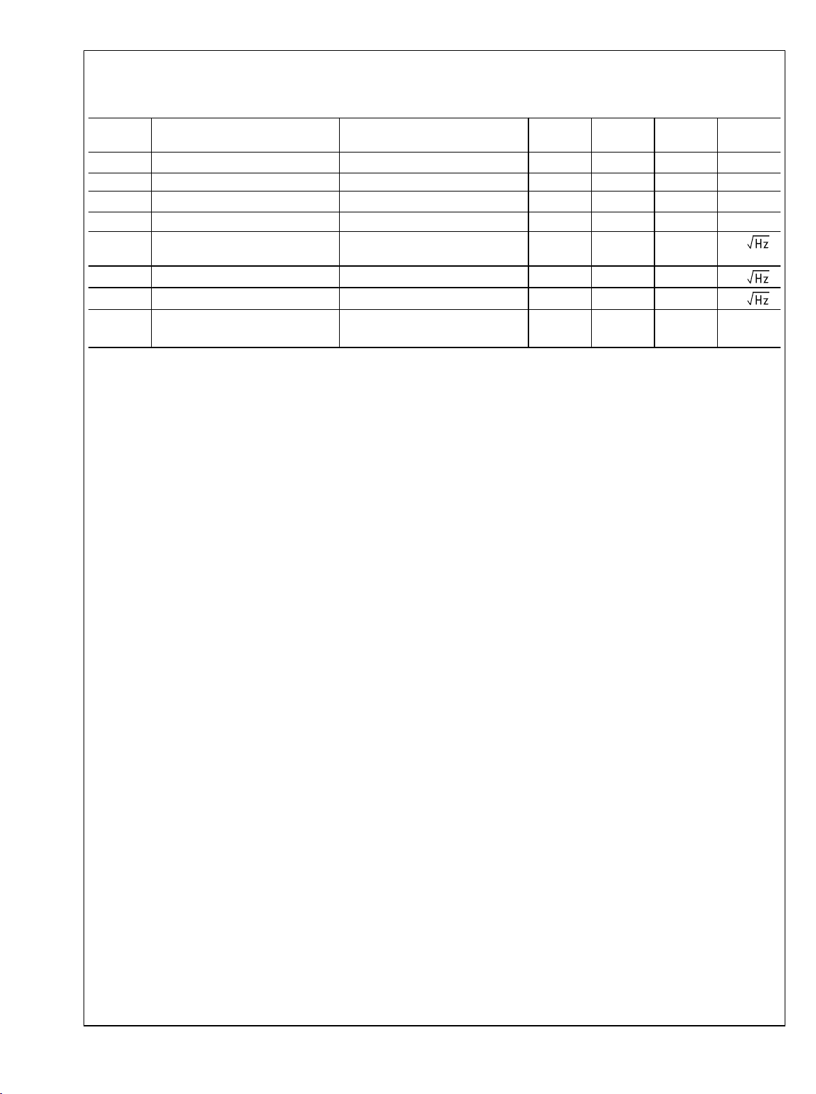
5.0V AC Electrical Characteristics (Note 13)
Unless otherwise specified, all limits are guaranteed for TA = 25°C. V+ = 5.0V, V − = 0V, VCM = V+/2, VO = V+/2 and RL > 1MΩ.
Boldface limits apply at the temperature extremes.
Symbol Parameter Conditions Min
(Note 7)
SR Slew Rate (Note 12)
AV = +1, RL = 10 kΩ
1.4 V/µs
GBW Gain-Bandwidth Product 3.5 MHz
Φ
m
G
m
LMV771/LMV772/LMV774
e
n
Phase Margin 79 Deg
Gain Margin −15 dB
Input-Referred Voltage Noise
f = 10kHz 6.5
(Flatband)
e
n
i
n
THD Total Harmonic Distortion f = 1kHz, AV = +1
Note 1: Absolute Maximum Ratings indicate limits beyond which damage to the device may occur. Operating Ratings indicate conditions for which the device is
intended to be functional, but specific performance is not guaranteed. For guaranteed specifications and the test conditions, see the Electrical Characteristics.
Note 2: Human Body Model is 1.5 kΩ in series with 100 pF. Machine Model is 0Ω in series with 20 pF.
Note 3: Shorting output to V+ will adversely affect reliability.
Note 4: Shorting output to V− will adversely affect reliability.
Note 5: The maximum power dissipation is a function of T
PD = (T
Note 6: Typical values represent the most likely parametric norm.
Note 7: All limits are guaranteed by testing or statistical analysis.
Note 8: Limits guaranteed by design.
Note 9: RL is connected to mid-supply. The output voltage is set at 200mV from the rails. VO = GND + 0.2V and VO = V+ −0.2V
Note 10: For LMV772/LMV774, temperature limits apply to −40°C to 85°C.
Note 11: For LMV772/LMV774, temperature limits apply to −40°C to 85°C. If RL is relaxed to 10 kΩ, then for LMV772/LMV774 temperature limits apply to −40°
C to 125°C.
Note 12: The number specified is the slower of positive and negative slew rates.
Note 13: Electrical Table values apply only for factory testing conditions at the temperature indicated. Factory testing conditions result in very limited self-heating
of the device such that TJ = TA.
Note 14: Continuous operation of the device with an output short circuit current larger than 35mA may cause permanent damage to the device.
Input-Referred Voltage Noise (l/f) f = 100Hz 12
Input-Referred Current Noise f = 1kHz 0.001
0.007 %
RL = 600Ω, VIN = 1 V
, θJA, and TA. The maximum allowable power dissipation at any ambient temperature is
)/θJA. All numbers apply for packages soldered directly into a PC board.
J(MAX)–T A
J(MAX)
PP
Typ
(Note 6)
Max
(Note 7)
Units
nV/
nV/
pA/
www.national.com 4
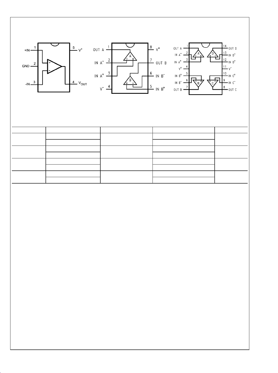
Connection Diagrams
LMV771/LMV772/LMV774
SC70-5
Top View
20039667
8-Pin MSOP/SOIC
Top View
20039671
14-Pin TSSOP
Top View
20039672
Ordering Information
Package Part Number Package Marking Transport Media NSC Drawing
SC70-5
8-Pin SOIC
8-Pin MSOP
14-Pin TSSOP
LMV771MG
LMV771MGX 3k Units Tape and Reel
LMV772MA
LMV772MAX 2.5k Units Tape and Reel
LMV772MM
LMV772MMX 3.5k Units Tape and Reel
LMV774MT
LMV774MTX 2.5k Units Tape and Reel
A75
LMV772MA
A91A
LMV774MT
1k Units Tape and Reel
95 Units/Rail
1k Units Tape and Reel
95 Units/Rail
MAA05A
M08A
MUA08A
MTC14
5 www.national.com

Typical Performance Characteristics
VOS vs. VCM Over Temperature
LMV771/LMV772/LMV774
Output Swing vs. V
VOS vs. VCM Over Temperature
20039627
S
Output Swing vs. V
20039626
S
20039625
Output Swing vs. V
S
20039623
www.national.com 6
20039624
IS vs. VS Over Temperature
20039630
 Loading...