

查询LMV1015供应商
LMV761/LMV762
Low Voltage, Precision Comparator with Push-Pull
Output
LMV761/LMV762 Low Voltage, Precision Comparator with Push-Pull Output
July 2002
General Description
The LMV761/762 are precision comparators intended for
applications requiring low noise and low input offset voltage.
The LV761 single has a shutdown pin that can be used to
disable the device and reduce the supply current. The
LMV761 is available in a space saving SOT23-6 or SOIC−8
package. The LMV762 dual is available in SOIC−8 or
MSOP-8 package.
They feature a CMOS input and Push-Pull output stage. The
Push-Pull output stage eliminates the need for an external
pull-up resistor.
The LMV761/762 are designed to meet the demands of
small size, low power and high performance required by
portable and battery operated electronics.
The input offset voltage has a typical value of 200µV at room
temp and a 1mV limit over temp.
Features
(VS=5V,TA= 25˚C, Typical values unless specified)
n Input offset voltage 0.2mV
n Input offset voltage (max over temp) 1mV
n Input bias current 0.2pA
n Propagation delay (OD = 50mV) 120 nsec
n Low supply current 300µA
n CMRR 100dB
n PSRR 110dB
n Extended Temperature Range −40˚C to 125˚C
n Push-pull output
n Ideal for 2.7V and 5V single supply applications
n Available in space-saving packages:
6-Pin SOT23 (single w/shutdown)
8-Pin SOIC (single w/shutdown)
8-Pin SOIC/MSOP (dual without shutdown)
Applications
n Portable and battery-powered systems
n Scanners
n Set top boxes
n High speed differential line receiver
n Window comparators
n Zero-crossing detectors
n High speed sampling circuits
Typical Circuit
20037032
Threshold Detector
© 2002 National Semiconductor Corporation DS200370 www.national.com
V
vs. V
OS
CC
20037010

Absolute Maximum Ratings (Note 1)
If Military/Aerospace specified devices are required,
please contact the National Semiconductor Sales Office/
Distributors for availability and specifications.
ESD Tolerance (Note 2)
LMV761/LMV762
Human Body Model 2000V
Machine Model 200V
+–V−
Supply Voltage (V
) 5.5V
Differential Input Voltage Supply Voltage
Voltage between any two pins Supply Voltage
Output Short Circuit to V
+-V−
Soldering Information
Wave Soldering (10 sec.) 260˚C (Lead Temp)
Junction Temperature 150˚C
Storage Temperature Range −65˚C to 150˚C
Operating Ratings
Supply Voltage (V+–V−) 2.7V to 5.0V
Temperature Range −40˚C to +125˚C
Package Thermal Resistance (Note 4)
SOT23-6 265˚C/W
SOIC-8 190˚C/W
MSOP-8 235˚C/W
Infrared or Convection (20 sec.) 235˚C
2.7V Electrical Characteristics
Unless otherwise specified, all limited guaranteed for TJ= 25˚C, VCM=V+/2, V+= 2.7V, V−=0V−. Boldface limits apply at the
temperature extremes. (Note 5)
Symbol Parameter Condition
V
OS
I
B
I
OS
CMRR Common Mode Rejection
Input Offset Voltage 0.2 1.0 mV
Input Bias Current (Note 8) 0.2 50 pA
Input Offset Current (Note 8) .001 5 pA
<
0V
<
V
VCC- 1.3V 80 100 dB
CM
Ratio
+
PSRR Power Supply Rejection Ratio V
CMVR Input Common Mode Voltage
= 2.7V to 5V 80 110 dB
>
CMRR
50dB −0.3
Range
V
O
I
SC
I
S
Output Swing High IL= 2mA, VID= 200mV V+– 0.35 V+– 0.1 V
Output Swing Low I
Output Short Circuit Current
(Note 3)
= −2mA, VID= −200mV 90 250 mV
L
Sourcing, VO= 1.35V, VID= 200mV 6.0 20
Sinking, V
= 1.35V, VID= −200mV 6.0 15
O
Supply Current
LMV762 (Both Comparators) 550 1400
I
OUT
LEAKAGE
I
S LEAKAGE
t
PD
t
SKEW
t
r
t
f
t
on
Output Leakage I@Shutdown SD = GND, VO= 2.7V 0.20 µA
Supply Leakage I@Shutdown SD = GND, VCC= 2.7V 0.20 2 µA
Propagation Delay
= 5.1kΩ
R
L
= 50pF
C
L
Overdrive = 5mV 270
Overdrive = 50mV 120
Propagation Delay Skew 5 ns
Output Rise Time 10% to 90% 1.7 ns
Output Fall Time 90% to 10% 1.8 ns
Turn On Time From Shutdown 6 µs
Min
(Note 7)
Typ
(Note 6)
Max
(Note 7) Units
1.5
V
mA
µALMV761 (Single Comparator) 275 700
nsOverdrive = 10mV 205
5.0V Electrical Characteristics
Unless otherwise specified, all limited guaranteed for TJ= 25˚C, VCM=V+/2, V+= 5.0V, V−=0V−. Boldface limits apply at the
temperature extremes.
Symbol Parameter Condition
V
OS
I
B
www.national.com 2
Input Offset Voltage 0.2 1.0 mV
Input Bias Current (Note 8) 0.2 50 pA
Min
(Note 7)
Typ
(Note 6)
Max
(Note 7) Units

5.0V Electrical Characteristics (Continued)
Unless otherwise specified, all limited guaranteed for TJ= 25˚C, VCM=V+/2, V+= 5.0V, V−=0V−. Boldface limits apply at the
temperature extremes.
Min
Symbol Parameter Condition
I
OS
CMRR Common Mode Rejection
Input Offset Current (Note 8) 0.01 5 pA
<
0V
<
V
VCC- 1.3V 80 100 dB
CM
(Note 7)
Ratio
PSRR Power Supply Rejection Ratio V+= 2.7V to 5V 80 110 dB
CMVR Input Common Mode Voltage
CMRR
>
50dB −.3
Range
V
O
I
SC
I
S
Output Swing High IL= 4mA, VID= 200mV V+– 0.35 V+– 0.1 V
Output Swing Low I
Output Short Circuit Current
(Note 3)
= −4mA, VID= −200mV 120 250 mV
L
Sourcing, VO= 2.5V, VID= 200mV 6.0 60
Sinking, V
= 2.5V, VID= −200mV 6.0 40
O
Supply Current
LMV762 (Both Comparators) 450 1400
I
OUT
LEAKAGE
I
S LEAKAGE
t
PD
t
SKEW
t
r
t
f
t
on
Note 1: Absolute Maximum Ratings indicate limits beyond which damage to the device may occur. Operating Ratings indicate conditions for which the device is
intended to be functional, but specific performance is not guaranteed. For guaranteed specifications and the test condition, see the Electrical Characteristics.
Note 2: Unless otherwise specified human body model is 1.5kΩ in series with 100pF. Machine model 200pF.
Note 3: Electrical Table values apply only for factory testing conditions at the temperature indicated. Factory testing conditions result in very limited self-heating of
the device such that T
See Application section for information on temperature de-rating of this device. Absolute Maximum Rating indicate junction temperature limits beyond which the
device may be permanently degraded, either mechanically or electrically.
Note 4: The maximum power dissipation is a function of T
P
=(T
D
Note 5: Maximum temperature guarantee range is −40˚C to 125˚C.
Note 6: Typical values represent the most likely parametric norm.
Note 7: All limits are guaranteed by testing or statistical analysis.
Note 8: Guaranteed by design
Output Leakage I@Shutdown SD = GND, VO= 5.0V 0.20 µA
Supply Leakage I@Shutdown SD = GND, VCC= 5.0V 0.20 2 µA
Propagation Delay
= 5.1kΩ
R
L
= 50pF
C
L
Overdrive = 5mV 225
Overdrive = 50mV 120
Propagation Delay Skew 5 ns
Output Rise Time 10% to 90% 1.7 ns
Output Fall Time 90% to 10% 1.5 ns
Turn On Time from Shutdown 4 µs
. No guarantee of parametric performance is indicated in the electrical tables under conditions of internal self-heating where T
J=TA
), θJA, and TA. The maximum allowable power dissipation at any ambient temperature is
J(MAX)-TA)θJA
. All numbers apply for packages soldered directly into a PC board.
J(MAX
Typ
(Note 6)
Max
(Note 7) Units
3.8
mA
µALMV761 (Single Comparator) 225 700
nsOverdrive = 10mV 190
>
J
LMV761/LMV762
V
TA.
www.national.com3

Connection Diagrams
LMV761
Single 6-Pin SOT23
LMV761/LMV762
Top View
Ordering Information
Package Part Number Package Marking Transport Media NSC Drawing
6-Pin SOT23 LMV761MF C22A 1k units Tape and Reel MF06A
8-Pin SOIC LMV761MA LMV761MA Rail M08A
8-Pin SOIC LMV762MA LMV762MA Rail M08A
8-Pin MSOP LMV762MM C23A 1k Units Tape and Reel MUA08A
LMV761
20037001
Single 8-Pin SOIC
20037002
Top View
Dual 8-Pin SOIC & MSOP
LMV761MFX 3k units Tape and Reel
LMV761MAX 2.5k Units Tape and Reel
LMV762MAX 2.5k Units Tape and Reel
LMV762MMX 3.5k Units Tape and Reel
LMV762
20037003
Top View
www.national.com 4

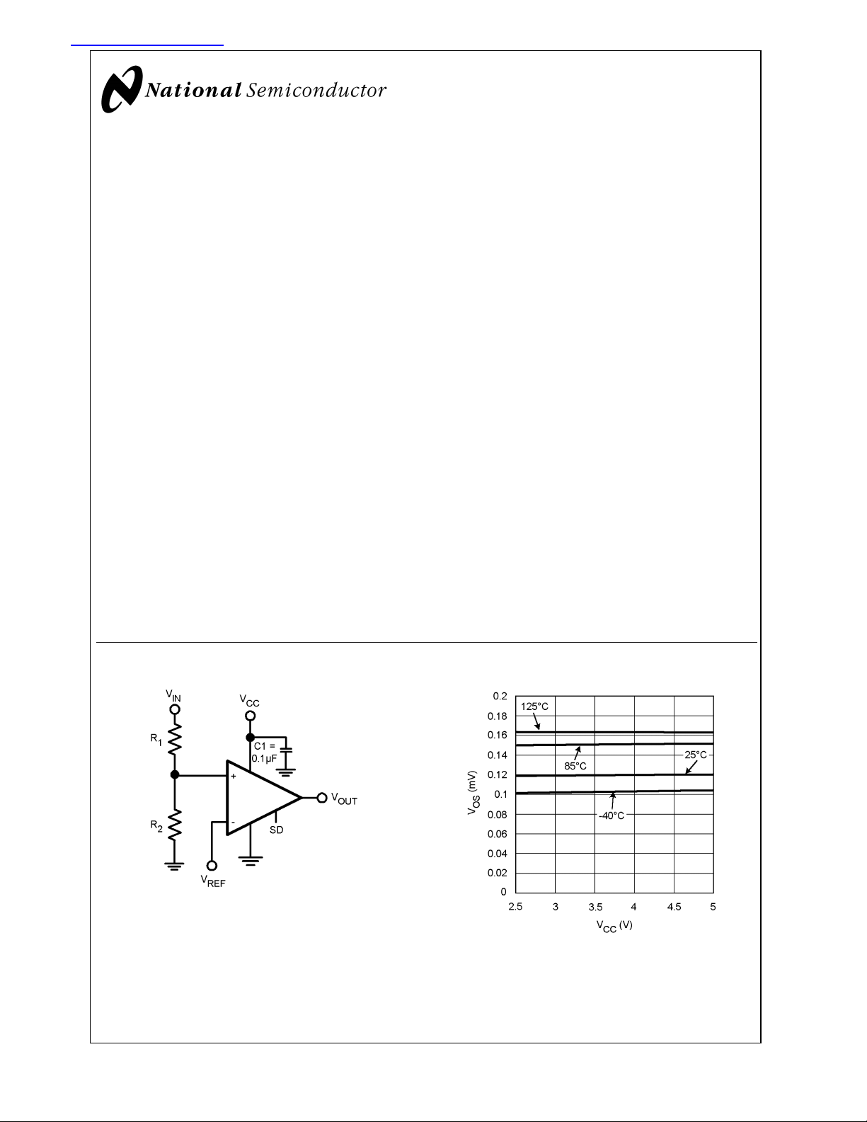
Typical Performance Characteristics
PSI vs. VCC(VO= High) PSI vs. VCC(VO= Low)
20037004 20037005
VOSvs. V
CC
LMV761/LMV762
Input Bias vs. Common Mode@25˚C
20037010
Input Bias vs. Common Mode@25˚C Output Voltage vs. Supply Voltage
20037025 20037011
20037024
www.national.com5

Typical Performance Characteristics (Continued)
Output Voltage vs. Supply Voltage Output Voltage vs. Supply Voltage
LMV761/LMV762
20037012 20037013
Output Voltage vs. Supply Voltage I
SOURCE
vs. V
OUT
20037014 20037006
I
vs. V
SINK
OUT
20037007
www.national.com 6
I
SOURCE
vs. V
OUT
20037008

Typical Performance Characteristics (Continued)
I
vs. V
SINK
OUT
LMV761/LMV762
Prop Delay vs. Overdrive
20037009
20037019
Response Time vs. Input Overdrives Positive Transition Response Time vs. Input Overdrives Positive Transition
20037020 20037021
Response Time vs. Input Overdrives Negative Transition Response Time vs. Input Overdrives Negative Transition
20037022
20037023
www.national.com7

Application Hints
Basic Comparator
A basic comparator circuit is used to convert analog input
signals to digital output signals. The comparator compares
an input voltage (V
ence voltage (V
LMV761/LMV762
the output (VO) is low (VOL). However, if VINis greater
V
REF
than V
, the output voltage (VO) is high (VOH).
REF
) at the non-inverting input to the refer-
IN
) at the inverting pin. If VINis less than
REF
20037028
20037026
20037031
FIGURE 1. Basic Comparator
Hysteresis
The basic comparator configuration may oscillate or produce
a noisy output if the applied differential input is near the
comparator’s input offset voltage. This tends to occur when
the voltage on one input is equal or very close to the other
input voltage. Adding hysteresis can prevent this problem.
Hysteresis creates two switching thresholds (one for the
rising input voltage and the other for the falling input voltage). Hysteresis is the voltage difference between the two
switching thresholds. When both inputs are nearly equal,
hysteresis causes one input to effectively move quickly past
the other. Thus, moving the input out of the region in which
oscillation may occur.
Hysteresis can easily be added to a comparator in a noninverting configuration with two resistors and positive feedback Figure 2. The output will switch from low to high when
rises up to V
V
IN
The output will switch from high to low when VINfalls to V
where V
IN2
The Hysteresis is the difference between V
= ((V
REF(R1+R2
, where V
IN1
=(V
V
IN1
is calculated by
=(V
V
IN2
REF(R1+R2
∆V
IN=VIN1-VIN2
))/R2)-((V
=V
is calculated by
IN1
REF(R1+R2
)–VCCR1)/R
REF(R1+R2
CCR1/R2
))/R
2
2
and V
IN1
))-(VCCR1))/R2)
IN2
IN2
.
20037027
FIGURE 2. Non-Inverting Comparator Configuration
Input
The LMV761/762 have near zero input bias current. This
allows very high resistance circuits to be used without any
concern for matching input resistances. This also allows the
use of very small capacitors in R-C type timing circuits. This
reduces the cost of the capacitors and amount of board
space used.
Shutdown Mode
The LMV761 features a low-power shutdown pin that is
activated by driving SD low. In shutdown mode, the output is
in a high impedance state, supply current is reduced to 20nA
and the comparator is disabled. Driving SD high will turn the
comparator on. The SD pin should not be left unconnected
due to the fact that it is a high impedance input. When left
unconnected, the output will be at an unknown voltage. Also
do not three-state the SD pin.
The maximum input voltage for SD is 5.5V, referred to
ground and is not limited by VCC. This allows the use of 5V
logic to drive SD while V
,
as 3V. The logic threshold limits for SD are proportional to
operates at a lower voltage, such
CC
VCC.
Board Layout and Bypassing
The LMV761/762 is designed to be stable and oscillation
free, but it is still important to include the proper bypass
capacitors and ground pickups. Ceramic 0.1µF capacitors
should be placed at both supplies to provide clean switching.
Minimize the length of signal traces to reduce stray capacitance.
www.national.com 8

Physical Dimensions inches (millimeters)
unless otherwise noted
LMV761/LMV762
6-Pin SOT23
NS Package Number MF06A
8-Pin SOIC
NS Package Number M08A
www.national.com9

Physical Dimensions inches (millimeters) unless otherwise noted (Continued)
8-Pin MSOP
NS Package Number MUA08A
LIFE SUPPORT POLICY
NATIONAL’S PRODUCTS ARE NOT AUTHORIZED FOR USE AS CRITICAL COMPONENTS IN LIFE SUPPORT
DEVICES OR SYSTEMS WITHOUT THE EXPRESS WRITTEN APPROVAL OF THE PRESIDENT AND GENERAL
LMV761/LMV762 Low Voltage, Precision Comparator with Push-Pull Output
COUNSEL OF NATIONAL SEMICONDUCTOR CORPORATION. As used herein:
1. Life support devices or systems are devices or
systems which, (a) are intended for surgical implant
into the body, or (b) support or sustain life, and
whose failure to perform when properly used in
accordance with instructions for use provided in the
2. A critical component is any component of a life
support device or system whose failure to perform
can be reasonably expected to cause the failure of
the life support device or system, or to affect its
safety or effectiveness.
labeling, can be reasonably expected to result in a
significant injury to the user.
National Semiconductor
Corporation
Americas
Email: support@nsc.com
www.national.com
National Semiconductor
Europe
Fax: +49 (0) 180-530 85 86
Email: europe.support@nsc.com
Deutsch Tel: +49 (0) 69 9508 6208
English Tel: +44 (0) 870 24 0 2171
Français Tel: +33 (0) 1 41 91 8790
National Semiconductor
Asia Pacific Customer
Response Group
Tel: 65-2544466
Fax: 65-2504466
Email: ap.support@nsc.com
National Semiconductor
Japan Ltd.
Tel: 81-3-5639-7560
Fax: 81-3-5639-7507
National does not assume any responsibility for use of any circuitry described, no circuit patent licenses are implied and National reserves the right at any time without notice to change said circuitry and specifications.
 Loading...