

查询LMV7271供应商
LMV7271/LMV7275/LMV7272
Single & Dual, 1.8V Low Power Comparators with
Rail-to-Rail Input
LMV7271/LMV7275/LMV7272 Single & Dual, 1.8V Low Power Comparators with Rail-to-Rail Input
September 2003
General Description
The LMV727X are rail-to-rail input low power comparators,
which are characterized at supply voltage 1.8V, 2.7V and
5.0V. They consume only 9uA supply current per channel
while achieving a 800ns propagation delay.
The LMV7271/LMV7275 (single) are available in SC70 and
SOT23 packages. The LMV7272 (dual) is available in micro
SMD package. With these tiny packages, the PC board area
can be significantly reduced. They are ideal for low voltage,
low power and space critical designs.
The LMV7271/LMV7272 both feature a push-pull output
stage which allows operation with minimum power consumption when driving a load. The LMV7275 features an open
drain output stage that allows for wired-OR configurations.
The open drain output also offers the advantage of allowing
the output to be pulled to any voltage up to 5V, regardless of
the supply voltage of the LMV7275.
The LMV727X are built with National Semiconductor’s advance submicron silicon-gate BiCMOS process. They all
have bipolar inputs for improved noise performance and
CMOS outputs for rail-to-rail output swing.
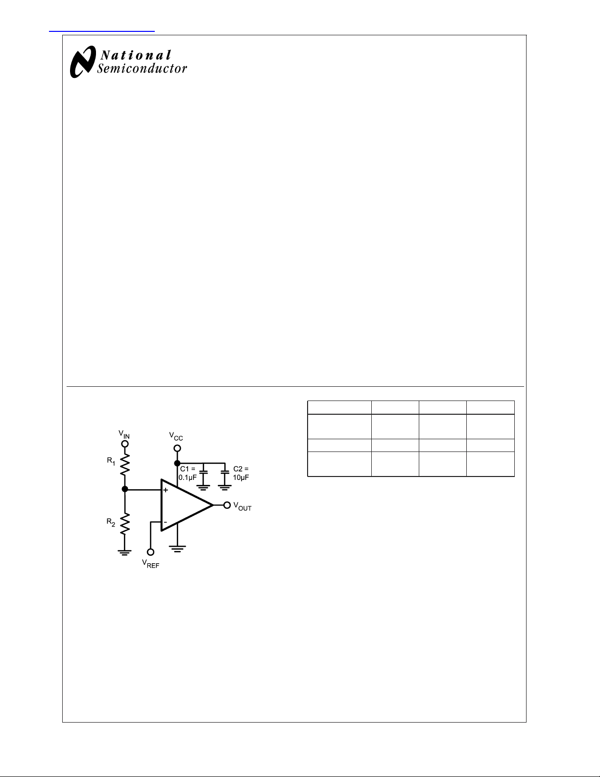
Typical Circuit
Features
(VS= 1.8V, TA= 25˚C, Typical values unless specified).
n Single or Dual Supplies
n Ultra low supply current 9µA per channel
n Low input bias current 10nA
n Low input offset current 200pA
n Low guaranteed V
n Propagation delay 880ns (20mV overdrive)
n Input common mode voltage range 0.1V beyond rails
n LMV7272 is available in micro SMD package
OS
4mV
Applications
n Mobile communications
n Laptops and PDA’s
n Battery powered electronics
n General purpose low voltage applications
Part Number Single/Dual Package Output
LMV7271 Single SC70,
SOT23
LMV7272 Dual micro SMD Push/Pull
LMV7275 Single SC70,
SOT23
Push/Pull
Open Drain
20064024
FIGURE 1. Threshold Detector
© 2003 National Semiconductor Corporation DS200640 www.national.com
Absolute Maximum Ratings (Note 1)
If Military/Aerospace specified devices are required,
Storage Temperature Range −65˚C to +150˚C
Junction Temperature (Note 4) +150˚C
please contact the National Semiconductor Sales Office/
Distributors for availability and specifications.
Operating Ratings (Note 1)
ESD Tolerance 2KV (Note 2)
Differential
V
IN
Supply Voltage (V
+-V−
) 5.5V
Voltage at Input/Output pins V
LMV7271/LMV7275/ LMV7272
Soldering Information
±
+
+0.1V, V−−0.1V
Infrared or Convection (20 sec.) 235˚C
Wave Soldering (10 sec.) 260˚C
200V (Note 6)
Supply Voltage
Operating Temperature Range
(Note 3) −40˚C to +85˚C
Package Thermal Resistance (Note 3)
SOT23-5 325˚C/W
SC-70 265˚C/W
8-Bump Thin micro SMD 220˚C/W
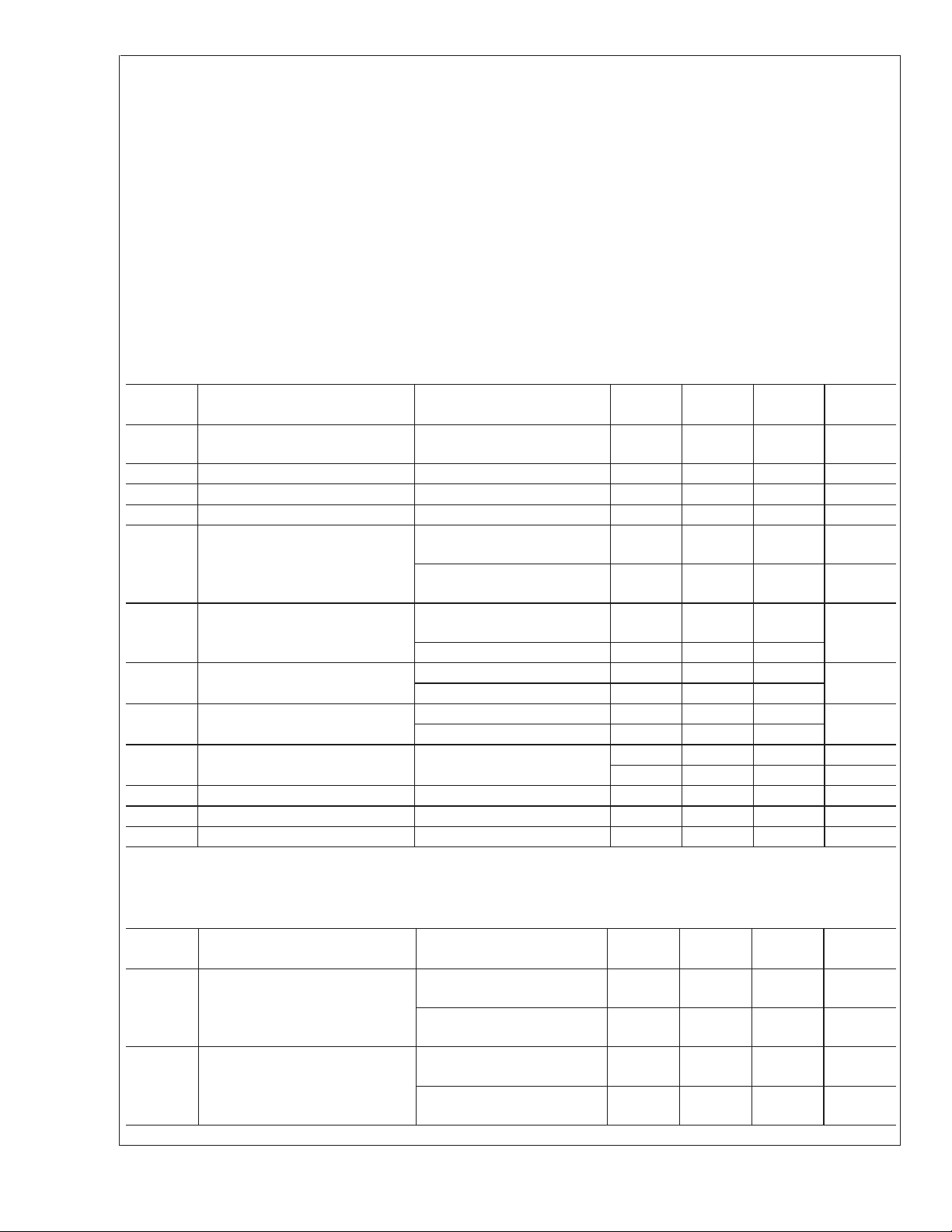
1.8V Electrical Characteristics
Unless otherwise specified, all limits guaranteed for TJ= 25˚C, V+= 1.8V, V−= 0V. Boldface limits apply at the temperature
extremes.
Symbol Parameter Condition Min
(Note 5)
V
OS
TC V
I
B
I
OS
I
S
Input Offset Voltage 0.3 4
Input Offset Temperature Drift VCM= 0.9V (Note 7) 20 uV/˚C
OS
Input Bias Current 10 nA
Input Offset Current 200 pA
Supply Current LMV7271/LMV7275 9 12
LMV7272 18 25
I
SC
Output Short Circuit Current Sourcing, VO= 0.9V
(LMV7271/LMV7272 only)
Sinking, V
V
OH
V
OL
V
CM
Output Voltage High
(LMV7271/LMV7272 only)
IO= 0.5mA 1.7 1.74
I
= 1.5mA 1.47 1.63
O
Output Voltage Low IO= −0.5mA 52 100
I
= −1.5mA 166 220
O
Input Common Mode Voltage
CMRR>45 dB 1.9 V
= 0.9V 4 6
O
Range
<
CMRR Common Mode Rejection Ratio 0
PSRR Power Supply Rejection Ratio V
I
LEAKAGE
Output Leakage Current VO= 1.8V (LMV7275 only) 2 pA
+
<
V
1.8V 46 78 dB
CM
= 1.8V to 5V 55 80 dB
3.5 6
−0.1 V
Typ
(Note 4)
Max
(Note 5)
6
14
28
Units
mV
µA
µA
mA
V
mV
1.8V AC Electrical Characteristics
Unless otherwise specified, all limits guaranteed for TJ= 25˚C, V+= 1.8V, V−= 0V, VCM= 0.5V, VO=V+/2 and R
−
. Boldface limits apply at the temperature extremes.
V
Symbol Parameter Condition Min
t
PHL
Propagation Delay
(High to Low)
Input Overdrive = 20mV
Load = 50pF//5kΩ
Input Overdrive = 50mV
Load = 50pF//5kΩ
t
PLH
Propagation Delay
(Low to High)
Input Overdrive = 20mV
Load = 50pF//5kΩ
Input Overdrive = 50mV
Load = 50pF//5kΩ
www.national.com 2
(Note 6)
Typ
(Note 5)
880 ns
570 ns
1100 ns
800 ns
Max
(Note 6)
L
>
1MΩ to
Units
2.7V Electrical Characteristics
Unless otherwise specified, all limits guaranteed for TJ= 25˚C, V+= 2.7V, V−= 0V. Boldface limits apply at the temperature
extremes.
Symbol Parameter Conditions Min
(Note 6)
V
OS
TC V
I
B
I
OS
I
S
Input Offset Voltage 0.3 4
Input Offset Temperature Drift VCM= 1.35V (Note 7) 20 µV/˚C
OS
Input Bias Current 10 nA
Input offset Current 200 pA
Supply Current LMV7271/LMV7275 9 13
LMV7272 18 25
I
SC
Output Short Circuit Current Sourcing, VO= 1.35V
(LMV7271/LMV7272 only)
= 1.35V 12 15
O
<
V
2.7V 46 78 dB
CM
V
OH
Output Voltage High
(LMV7271/LMV7272 only)
V
OL
V
CM
Output Voltage Low IO= −0.5mA 50 70
Input Common Voltage Range CMRR>45dB 2.8 V
CMRR Common Mode Rejection Ratio 0
PSRR Power Supply Rejection Ratio V
I
LEAKAGE
Output Leakage Current VO= 2.7V (LMV7275 only) 2 pA
Sinking, V
IO= 0.5mA 2.63 2.66
I
= 2.0mA 2.48 2.55
O
I
= −2mA 155 220
O
<
+
= 1.8V to 5V 55 80 dB
12 15
−0.1 V
Typ
(Note 5)
Max
(Note 6)
6
15
28
LMV7271/LMV7275/ LMV7272
Units
mV
µA
µA
mA
V
mV
2.7V AC Electrical Characteristics
Max
L
>
1MΩ to
Units
Unless otherwise specified, all limits guaranteed for TJ= 25˚C, V+= 2.7V, V−= 0V, VCM= 0.5V, VO=V+/2 and R
−
. Boldface limits apply at the temperature extremes.
V
Symbol Parameter Condition Min
(Note 6)
t
PHL
Propagation Delay
(High to Low)
Input Overdrive = 20mV
Load = 50pF//5kΩ
Input Overdrive = 50mV
Typ
(Note 5)
(Note 6)
1200 ns
810 ns
Load = 50pF//5kΩ
t
PLH
Propagation Delay
(Low to High)
Input Overdrive = 20mV
Load = 50pF//5kΩ
Input Overdrive = 50mV
1300 ns
860 ns
Load = 50pF//5kΩ
5.0V Electrical Characteristics
Unless otherwise specified, all limits guaranteed for TJ= 25˚C, V+= 5V, V−= 0V. Boldface limits apply at the temperature extremes.
Symbol Parameter Conditions Min
(Note 6)
V
OS
TC V
I
B
I
OS
Input Offset Voltage 0.3 4
Input Offset Temperature Drift VCM= 2.5V (Note 7) 20 µV/˚C
OS
Input Bias Current 10 nA
Input Offset Current 200 pA
Typ
(Note 5)
Max
(Note 6)
6
Units
mV
www.national.com3
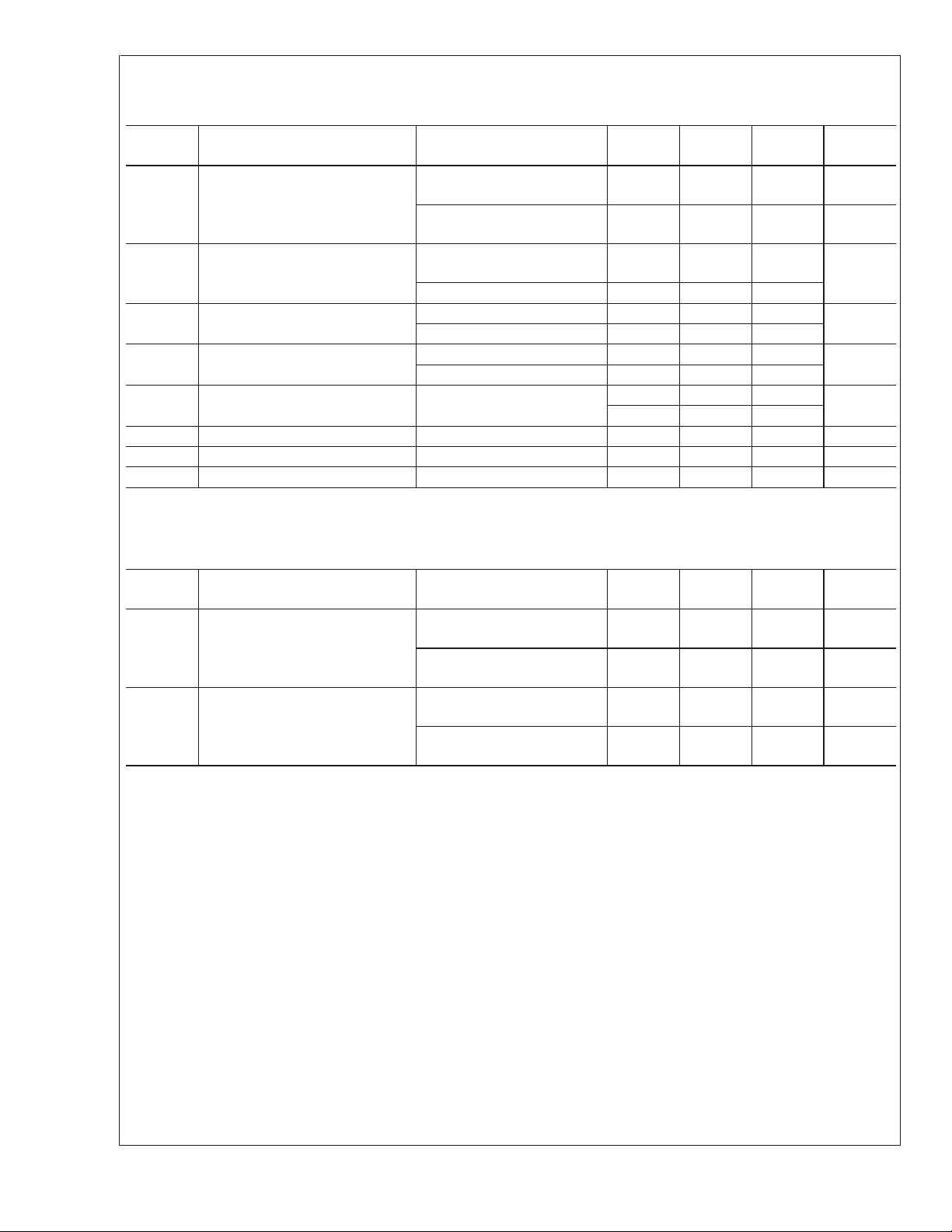
5.0V Electrical Characteristics (Continued)
Unless otherwise specified, all limits guaranteed for TJ= 25˚C, V+= 5V, V−= 0V. Boldface limits apply at the temperature extremes.
Symbol Parameter Conditions Min
(Note 6)
I
S
Supply Current LMV7271/LMV7275 10 14
Typ
(Note 5)
Max
(Note 6)
16
LMV7272 20 27
30
I
SC
LMV7271/LMV7275/ LMV7272
Output Short Circuit Current Sourcing, VO= 2.5V
(LMV7271/LMV7272 only)
28 34
Sinking, VO= 2.5V 28 34
V
OH
V
OL
V
CM
Output Voltage High
(LMV7271/LMV7272 only)
IO= 0.5mA 4.93 4.96
I
= 4.0mA 4.70 4.77
O
Output Voltage Low IO= −0.5mA 27 70
I
= −4.0mA 225 300
O
Input Common Voltage Range CMRR>45dB 5.1
−0.1
<
CMRR Common Mode Rejection Ratio 0
PRSS Power Supply Rejection Ratio V
I
LEAKAGE
Output Leakage Current VO= 5V (LMV7275 only) 2 pA
+
<
V
5.0V 46 78 dB
CM
= 1.8V to 5V 55 80 dB
5.0V AC Electrical Characteristics
Unless otherwise specified, all limits guaranteed for TJ= 25˚C, V+= 5.0V, V−= 0V, VCM= 0.5V, VO=V+/2 and R
−
. Boldface limits apply at the temperature extremes.
V
Symbol Parameter Condition Min
(Note 6)
t
PHL
Propagation Delay
(High to Low)
Input Overdrive = 20mV
Load = 50pF//5kΩ
Input Overdrive = 50mV
Load = 50pF//5kΩ
t
PLH
Propagation Delay
(Low to High)
Input Overdrive = 20mV
Load = 50pF//5kΩ
Input Overdrive = 50mV
Load = 50pF//5kΩ
Note 1: Absolute Maximum Ratings indicate limits beyond which damage to the device may occur. Operating Ratings indicate conditions for which the device is
intended to be functional, but specific performance is not guaranteed. For guaranteed specifications and the test conditions, see the Electrical Characteristics.
Note 2: Human body model, 1.5kΩ in series with 100pF.
Note 3: The maximum power dissipation is a function of T
P
=(T
D
J(MAX)-TA
Note 4: Typical values represent the most likely parametric norm.
Note 5: All limits are guaranteed by testing or statistical analysis.
Note 6: Machine Model, 0Ω in series with 200pF.
Note 7: Offset Voltage average drift determined by dividing the change in V
Note 8: Electrical Table values apply only for factory testing conditions at the temperature indicated. Factory testing conditions result in very limited self-heating of
the device such that T
Absolute Maximum Ratings indicate junction temperature limits beyond which the device may be permanently degraded, either mechanically or electrically.
)/θJA. All numbers apply for packages soldered directly into a PC board.
. No guarantee of parametric performance is indicated in the electrical tables under conditions of internal self heating where T
J=TA
, θJA, and TA. The maximum allowable power dissipation at any ambient temperature is
J(MAX)
at temperature extremes into the total temperature change.
OS
Typ
(Note 5)
Max
(Note 6)
2100 ns
1380 ns
1800 ns
1100 ns
L
>
1MΩ to
Units
µA
µA
mA
V
mV
V
Units
>
J
TA.
www.national.com 4
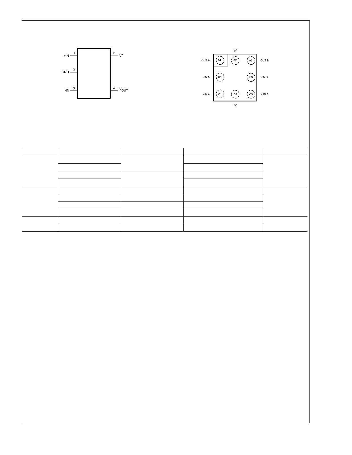
Connection Diagrams
5-Pin SOT23/SC70 (LMV7271/LMV7275) 8-Bump micro SMD (LMV7272)
LMV7271/LMV7275/ LMV7272
Top View
20064023
20064041
Top View
(bump side down)
Ordering Information
Package Part Number Package Marking Transport Media NSC Drawing
5-Pin SOT23 LMV7271MF C25A 1k Units Tape and Reel MF05A
LMV7271MFX 3k Units Tape and Reel
LMV7275MF C26A 1k Units Tape and Reel
LMV7275MFX 3k Units Tape and Reel
5-Pin SC70 LMV7271MG C34 1k Units Tape and Reel MAA05A
LMV7271MGX 3k Units Tape and Reel
LMV7275MG C35 1k Units Tape and Reel
LMV7275MGX 3k Units Tape and Reel
8-Bump
micro SMD
LMV7272TL I 01 250 Units Tape and Reel TLA08AAA
LMV7272TLX 3k Units Tape and Reel
www.national.com5

Typical Performance Characteristics
(TA= 25˚C, Unless otherwise specified).
LMV7271/LMV7275/ LMV7272
vs. V
V
OS
VOSvs. V
CM
CM
VOSvs. V
20064028 20064029
CM
Short Circuit vs. Supply Voltage
20064030
Supply Current vs. Supply Voltage (LMV7271) Supply Current vs. Supply Voltage (LMV7272)
20064002
www.national.com 6
20064001
20064031

LMV7271/LMV7275/ LMV7272
Typical Performance Characteristics (T
= 25˚C, Unless otherwise specified). (Continued)
A
Supply Current vs. Supply Voltage (LMV7272) Output Positive Swing vs. V
20064032
Output Negative Swing vs. V
SUPPLY
Output Positive Swing vs. I
SUPPLY
20064033
SOURCE
Output Negative Swing vs. I
20064034
SINK
20064036 20064037
Output Positive Swing vs. I
SOURCE
20064035
www.national.com7

Typical Performance Characteristics (T
= 25˚C, Unless otherwise specified). (Continued)
A
LMV7271/LMV7275/ LMV7272
Output Negative Swing vs. I
Output Positive Swing vs. I
SINK
SOURCE
20064038
Output Negative Swing vs. I
Propagation Delay (t
PLH
SINK
20064039
)
20064040
Propagation Delay (t
) Propagation Delay (t
PHL
20064018
www.national.com 8
PLH
20064014
)
20064015

LMV7271/LMV7275/ LMV7272
Typical Performance Characteristics (T
Propagation Delay (t
Propagation Delay (t
) Propagation Delay (t
PHL
20064020 20064016
)t
PHL
= 25˚C, Unless otherwise specified). (Continued)
A
)
PLH
vs. Overdrive
PHL
t
vs. Overdrive
PLH
20064022
20064049
20064050
www.national.com9

Application Notes
BASIC COMPARATOR
A comparator is often used to convert an analog signal to a
digital signal. As shown in Figure 2, the comparator compares an input voltage (V
LMV7271/LMV7275/ LMV7272
) to a reference voltage (V
IN
LMV7271
20064025
FIGURE 2. LMV7271 Basic Comparator
REF
). If
V
is less than V
IN
is greater than V
, the output (VO) is low. However, if V
REF
, the output voltage (VO) is high.
REF
IN
20064017
RAIL-TO-RAIL INPUT STAGE
The LMV727X has an input common mode voltage range
) of −0.1V below the V−to 0.1V above V+. This is
(V
CM
achieved by using paralleled PNP and NPN differential input
pairs. When the V
PNP pair is off. When the V
and the PNP pair is on. The crossover point between the
NPN and PNP input stages is around 950mV from V
each input stage has its own offset voltage (V
the comparator becomes a function of the V
for V
vs. VCMin Typical Performance Characteristics sec-
OS
is near V+, the NPN pair is on and the
CM
is near V−, the NPN pair is off
CM
), the VOSof
OS
. See curves
CM
+
. Since
tion. In application design, it is recommended to keep the
away from the crossover point to avoid problems. The
V
CM
wide input voltage range makes LMV727X ideal in power
supply monitoring circuits, where the comparators are used
to sense signals close to ground and power supplies.
OUTPUT STAGE
The LMV7271 and LMV7272 have a push-pull output stage.
This output stage keeps the total system power consumption
to the absolute minimum. The only current consumed is the
low supply current and the current going directly into the
load. When the output switches, both PMOS and NMOS at
the output stage are on at the same time for a very short
time. This allows current to flow directly between V
+
and V
through output transistors. The result is a short spike of
current (shoot-through current) drawn from the supply and
glitches in the supply voltages. The glitches can spread to
other parts of the board as noise. To prevent the glitches in
supply lines, power supply bypass capacitors must be installed. See section for supply bypassing in the Application
Notes for details.
HYSTERESIS
It is a standard procedure to use hysteresis (positive feedback) around a comparator, to prevent oscillation, and to
avoid excessive noise on the output because the comparator
is a good amplifier of its own noise.
Inverting Comparator with Hysteresis
The inverting comparator with hysteresis requires a three
resistor network that is referenced to the supply voltage V
CC
of the comparator (Figure 3). When VINat the inverting input
is less than V
comparator (V
plicity assume V
network resistors can be represented as R
. The lower input trip voltage VA1is defined as
R
2
When VINis greater than VA(V
, the voltage at the non-inverting node of the
A
<
VA), the output voltage is high (for sim-
IN
switches as high as VCC). The three
O
>
IN
||R3in series with
1
VA), the output voltage is
low and very close to ground. In this case the three network
resistors can be presented as R
−
upper trip voltage V
is defined as
A2
//R3in series with R1. The
2
The total hysteresis provided by the network is defined as
∆V
A=VA1-VA2
A good typical value of ∆VAwould be in the range of 5 to
50mV. This is easily obtained by choosing R
times (R
(R
||R2) for 5V operation, or as 300 to 30 times
1
||R2) for 1.8V operation.
1
as 1000 to 100
3
www.national.com 10

Application Notes (Continued)
LMV7271/LMV7275/ LMV7272
FIGURE 3. Inverting Comparator with Hysteresis
Non-Inverting Comparator with Hysteresis
A non-inverting comparator with hysteresis requires a two
resistor network, and a voltage reference (V
verting input (Figure 4). When V
is low, the output is also
IN
low. For the output to switch from low to high, V
up to V
, where V
IN1
is calculated by
IN1
) at the in-
REF
IN
must rise
20064042
When VINis high, the output is also high. To make the
comparator switch back to its low state, V
before VAwill again equal V
REF.VIN
The hysteresis of this circuit is the difference between V
and V
IN2
.
∆V
IN=VCCR1/R2
must equal V
IN
REF
can be calculated by:
IN1
www.national.com11

Application Notes (Continued)
LMV7271/LMV7275/ LMV7272
FIGURE 4. Non-Inverting Comparator with Hysteresis
CIRCUIT TECHNIQUES FOR AVOIDING OSCILLATIONS
IN COMPARATOR APPLICATIONS
Feedback to almost any pin of a comparator can result in
oscillation. In addition, when the input signal is a slow voltage ramp or sine wave, the comparator may also burst into
oscillation near the crossing point. To avoid oscillation or
instability, PCB layout should be engineered thoughtfully.
Several precautions are recommended:
1. Power supply bypassing is critical, and will improve stability and transient response. Resistance and inductance
from power supply wires and board traces increase
power supply line impedance. When supply current
changes, the power supply line will move due to its impedance. Large enough supply line shift will cause the
comparator to mis-operate. To avoid problems, a small
bypass capacitor, such as 0.1uF ceramic, should be
placed immediately adjacent to the supply pins. An additional 6.8µF or greater tantalum capacitor should be
placed at the point where the power supply for the comparator is introduced onto the board. These capacitors
act as an energy reservoir and keep the supply impedance low. In dual supply application, a 0.1µF capacitor is
recommended to be placed across V
2. Keep all leads short to reduce stray capacitance and lead
inductance. It will also minimize any unwanted coupling
from any high-level signals (such as the output). The
comparators can easily oscillate if the output lead is
inadvertently allowed to capacitively couple to the inputs
via stray capacitance. This shows up only during the
output voltage transition intervals as the comparator
changes states. Try to avoid a long loop which could act
as an inductor (coil).
3. It is a good practice to use an unbroken ground plane on
a printed circuit board to provide all components with a
+
and V−pins.
20064044
20064043
low inductive ground connection. Make sure ground
paths are low-impedance where heavier currents are
flowing to avoid ground level shift. Preferably there
should be a ground plane under the component.
4. The output trace should be routed away from inputs. The
ground plane should extend between the output and
inputs to act as a guard. This can be achieved by running
a topside ground plane between the output and inputs. A
typical PCB layout is shown in Figure 5.
20064051
FIGURE 5. Typical PCB Layout
5. When the signal source is applied through a resistive
network to one input of the comparator, it is usually
advantageous to connect the other input with a resistor
with the same value, for both DC and AC consideration.
Input traces should be laid out symmetrically if possible.
6. All pins of any unused comparators should be tied to the
negative supply.
micro SMD LIGHT SENSITIVITY
Exposing the micro SMD device to direct sunlight will cause
mis-operation of the device. Light sources such as Halogen
lamps can also affect electrical performance if brought near
to the device. The wavelengths, which have the most detrimental effect, are reds and infrareds.
micro SMD MOUNTING
The micro SMD package requires specific mounting techniques, which are detailed in National Semiconductor Application Note AN-1112.
LMV7272 micro SMD to DIP Conversion Board
To facilitate characterization and testing, a micro SMD to DIP
conversion board, LMV7272TLCONV, is available. It is a
2-layer board, with the LMV7272 mounted on the bottom
layer, and a capacitor (C1, between the positive and negative supplies) added to the top layer.
20064060
LMV7272TLCONV Diagram
www.national.com 12

LMV7271/LMV7275/ LMV7272
Typical Applications
UNIVERSAL LOGIC LEVEL SHIFTER
The output of LMV7275 is an unconnected drain of an
NMOS device, which can be pulled up, through a resistor, to
any desired output level within the permitted power supply
range. Hence, the following simple circuit works as a universal logic level shifter, pulling up the signal to the desired
level.
20064052
FIGURE 6. Logic Level Shifter
POSITIVE PEAK DETECTOR
A positive peak detect circuit is basically a comparator operated in a unity gain follower configuration, with a capacitor as
a load to maintain the highest voltage. A diode is added at
the output to prevent the capacitor from discharging through
the pull-up resistor, and a 1MΩ resistor added in parallel to
the capacitor to provide a high impedance discharge path.
When the input V
comparator follows it, thus charging the capacitor. When it
decreases, the cap discharges through the 1MΩ resistor.
The decay time can be modified by changing the resistor.
The output should be accessed through a follower circuit to
prevent loading.
increases, the inverting input of the
IN
OR’ING THE OUTPUT
Since the output is an unconnected NMOS drain, many
drains can be tied together, pulled up to V
by a single
DD
resistor to provide an output OR’ing function. If any of the
comparator outputs is pulled low the output V
goes down.
O
FIGURE 7. Positive Peak Detector
20064053
FIGURE 8. OR’ing the Outputs
20064054
www.national.com13

Typical Applications (Continued)
NEGATIVE PEAK DETECTOR
For the negative detector, the output transistor of the comparator acts as a low impedance current sink. Since there is
no pull-up resistor, the only discharge path will be the 1MΩ
resistor and any load impedance used. Decay time is
changed by varying the 1MΩ resistor.
LMV7271/LMV7275/ LMV7272
FIGURE 9. Negative Peak Detector
SQUARE WAVE GENERATOR
A typical application for a comparator is as a square wave
oscillator. The circuit below generates a square wave whose
period is set by the RC time constant of the capacitor C
resistor R
signal propagation delay of the comparator, and by the capacitive loading at the output, which limits the output slew
rate.
. The maximum frequency is limited by the large
4
20064055
1
20064056
and
20064057
FIGURE 10. Squarewave Oscillator
To analyze the circuit, consider it when the output is high.
That implies that the inverted input (V
non-inverting input (V
through R
and the voltage VCincreases till it is equal to the
4,
). This causes the C1to get charged
A
non-inverting input. The value of V
) is lower than the
C
at this point is
A
If R1=R2=R3then VA1=2VCC/3
At this point the comparator switches pulling down the output
to the negative rail. The value of V
at this point is
A
If R1=R2=R3then VA2=VCC/3
The capacitor C
age V
decreases till it is equal to VA2, at which point the
C
now discharges through R4, and the volt-
1
comparator switches again, bringing it back to the initial
stage. The time period is equal to twice the time it takes to
discharge C
.ln2. Hence the formula for the frequency is:
R
4C1
F = 1/(2·R
from 2VCC/3 to VCC/3, which is given by
1
·ln2)
4·C1
www.national.com 14

Physical Dimensions inches (millimeters) unless otherwise noted
5-Pin SOT23-5
NS Package Number MF05A
LMV7271/LMV7275/ LMV7272
5-Pin SC70-5
NS Package Number MAA05A
www.national.com15

Physical Dimensions inches (millimeters) unless otherwise noted (Continued)
NOTE: UNLESS OTHERWISE SPECIFIED
1. EPOXY COATING
2. 63Sn/37Pb EUTECTIC BUMP
3. RECOMMEND NON-SOLDER MASK DEFINED LANDING PAD.
4. PIN A1 IS ESTABLISHED BY LOWER LEFT CORNER WITH RESPECT TO TEXT ORIENTATION REMAINING PINS ARE NUMBERED
COUNTERCLOCKWISE.
5. XXX IN DRAWING NUMBER REPRESENTS PACKAGE SIZE VARIATION WHERE X1 IS PACKAGE WIDTH, X2 IS PACKAGE LENGTH AND X3 IS
PACKAGE HEIGHT.
6. REFERENCE JEDEC REGISTRATION MO-211, VARIATION BC.
8-Bump micro SMD
NS Package Number TLA08AAA
X1 = 1.514mm X2 = 1.514mm X3 = 0.600mm
LIFE SUPPORT POLICY
NATIONAL’S PRODUCTS ARE NOT AUTHORIZED FOR USE AS CRITICAL COMPONENTS IN LIFE SUPPORT
DEVICES OR SYSTEMS WITHOUT THE EXPRESS WRITTEN APPROVAL OF THE PRESIDENT AND GENERAL
COUNSEL OF NATIONAL SEMICONDUCTOR CORPORATION. As used herein:
1. Life support devices or systems are devices or
systems which, (a) are intended for surgical implant
into the body, or (b) support or sustain life, and
whose failure to perform when properly used in
accordance with instructions for use provided in the
2. A critical component is any component of a life
support device or system whose failure to perform
can be reasonably expected to cause the failure of
the life support device or system, or to affect its
safety or effectiveness.
labeling, can be reasonably expected to result in a
significant injury to the user.
National Semiconductor
Americas Customer
Support Center
Email: new.feedback@nsc.com
Tel: 1-800-272-9959
www.national.com
LMV7271/LMV7275/LMV7272 Single & Dual, 1.8V Low Power Comparators with Rail-to-Rail Input
National does not assume any responsibility for use of any circuitry described, no circuit patent licenses are implied and National reserves the right at any time without notice to change said circuitry and specifications.
National Semiconductor
Europe Customer Support Center
Fax: +49 (0) 180-530 85 86
Email: europe.support@nsc.com
Deutsch Tel: +49 (0) 69 9508 6208
English Tel: +44 (0) 870 24 0 2171
Français Tel: +33 (0) 1 41 91 8790
National Semiconductor
Asia Pacific Customer
Support Center
Email: ap.support@nsc.com
National Semiconductor
Japan Customer Support Center
Fax: 81-3-5639-7507
Email: jpn.feedback@nsc.com
Tel: 81-3-5639-7560
 Loading...