

Page 1
查询LMV321供应商
LMV321/LMV358/LMV324 Single/Dual/Quad
General Purpose, Low Voltage, Rail-to-Rail Output
Operational Amplifiers
June 2003
LMV321/LMV358/LMV324 Single/Dual/Quad General Purpose, Low Voltage, Rail-to-Rail Output
Operational Amplifiers
General Description
The LMV358/324 are low voltage (2.7–5.5V) versions of the
dual and quad commodity op amps, LM358/324, which currently operate at 5–30V. The LMV321 is the single version.
The LMV321/358/324 are the most cost effective solutions
for the applications where low voltage operation, space saving and low price are needed. They offer specifications that
meet or exceed the familiar LM358/324. The LMV321/358/
324 have rail-to-rail output swing capability and the input
common-mode voltage range includes ground. They all exhibit excellent speed-power ratio, achieving 1MHz of bandwidth and 1V/µs of slew rate with low supply current.
The LMV321 is available in space saving SC70-5, which is
approximately half the size of SOT23-5. The small package
saves space on pc boards, and enables the design of small
portable electronic devices. It also allows the designer to
place the device closer to the signal source to reduce noise
pickup and increase signal integrity.
The chips are built with National’s advanced submicron
silicon-gate BiCMOS process. The LMV321/358/324 have
bipolar input and output stages for improved noise performance and higher output current drive.
Gain and Phase vs. Capacitive Load
Features
(For V+= 5V and V−= 0V, Typical Unless Otherwise Noted)
n Guaranteed 2.7V and 5V Performance
n No Crossover Distortion
n Space Saving Package SC70-5 2.0x2.1x1.0mm
n Industrial Temp. Range −40˚C to +85˚C
n Gain-Bandwidth Product 1MHz
n Low Supply Current
— LMV321 130µA
— LMV358 210µA
— LMV324 410µA
n Rail-to-Rail Output Swing
n V
CM
@
10kΩ V+−10mV
−0.2V to V+−0.8V
−
V
+65mV
Applications
n Active Filters
n General Purpose Low Voltage Applications
n General Purpose Portable Devices
Output Voltage Swing vs. Supply Voltage
10006045
© 2003 National Semiconductor Corporation DS100060 www.national.com
10006067
Page 2
Absolute Maximum Ratings (Note 1)
If Military/Aerospace specified devices are required,
Storage Temp. Range −65˚C to 150˚C
Junction Temperature(Note 5) 150˚C
please contact the National Semiconductor Sales Office/
Distributors for availability and specifications.
Operating Ratings (Note 1)
ESD Tolerance (Note 2)
Machine Model 100V
Human Body Model
LMV358/324 2000V
LMV321 900V
Differential Input Voltage
Supply Voltage (V
Output Short Circuit to V
Output Short Circuit to V
+–V−
) 5.5V
+
−
Soldering Information
Infrared or Convection (20 sec) 235˚C
LMV321/LMV358/LMV324 Single/Dual/Quad
±
Supply Voltage
(Note 3)
(Note 4)
Supply Voltage 2.7V to 5.5V
Temperature Range
LMV321, LMV358, LMV324 −40˚C to +85˚C
Thermal Resistance (θ
)(Note 10)
JA
5-pin SC70-5 478˚C/W
5-pin SOT23-5 265˚C/W
8-Pin SOIC 190˚C/W
8-Pin MSOP 235˚C/W
14-Pin SOIC 145˚C/W
14-Pin TSSOP 155˚C/W
2.7V DC Electrical Characteristics
Unless otherwise specified, all limits guaranteed for TJ= 25˚C, V+= 2.7V, V−= 0V, VCM= 1.0V, VO=V+/2 and R
Symbol Parameter Conditions
V
OS
TCV
Input Offset Voltage 1.7 7 mV
Input Offset Voltage Average
OS
Typ
(Note 6)
5 µV/˚C
Limit
(Note 7) Units
Drift
I
B
I
OS
Input Bias Current 11 250 nA
Input Offset Current 5 50 nA
CMRR Common Mode Rejection Ratio 0V ≤ VCM≤ 1.7V 63 50 dB
PSRR Power Supply Rejection Ratio 2.7V ≤ V
=1V
V
O
V
CM
Input Common-Mode Voltage
For CMRR≥50dB −0.2 0 V
+
≤ 5V
60 50 dB
Range
1.9 1.7 V
V
O
Output Swing RL= 10kΩ to 1.35V V+-10 V+-100 mV
60 180 mV
I
S
Supply Current LMV321 80 170 µA
LMV358
140 340 µA
Both amplifiers
LMV324
260 680 µA
All four amplifiers
L
>
1MΩ.
max
max
max
min
min
min
max
min
max
max
max
max
www.national.com 2
Page 3
2.7V AC Electrical Characteristics
Unless otherwise specified, all limits guaranteed for TJ= 25˚C, V+= 2.7V, V−= 0V, VCM= 1.0V, VO=V+/2 and R
Symbol Parameter Conditions
GBWP Gain-Bandwidth Product C
Φ
m
G
m
e
n
Phase Margin 60 Deg
Gain Margin 10 dB
Input-Referred Voltage Noise f = 1kHz 46
= 200pF 1 MHz
L
Typ
(Note 6)
Limit
(Note 7)
LMV321/LMV358/LMV324 Single/Dual/Quad
>
1MΩ.
L
Units
i
n
Input-Referred Current Noise f = 1kHz 0.17
5V DC Electrical Characteristics
Unless otherwise specified, all limits guaranteed for TJ= 25˚C, V+= 5V, V−= 0V, VCM= 2.0V, VO=V+/2 and R
Boldface limits apply at the temperature extremes.
Symbol Parameter Conditions
V
OS
Input Offset Voltage 1.7 7
Typ
(Note 6)
Limit
(Note 7) Units
9
TCV
Input Offset Voltage Average
OS
5 µV/˚C
Drift
I
B
Input Bias Current 15 250
500
I
OS
Input Offset Current 5 50
150
CMRR Common Mode Rejection Ratio 0V ≤ VCM≤ 4V 65 50 dB
PSRR Power Supply Rejection Ratio 2.7V ≤ V
=1VVCM=1V
V
O
V
CM
Input Common-Mode Voltage
For CMRR≥50dB −0.2 0 V
+
≤ 5V
60 50 dB
Range
4.2 4 V
A
V
Large Signal Voltage Gain (Note8)RL=2kΩ 100 15
10
V
O
Output Swing RL=2kΩ to 2.5V V+-40 V+-300
+
-400
V
120 300
400
R
= 10kΩ to 2.5V V+-10 V+-100
L
+
-200
V
65 180
280
I
O
Output Short Circuit Current Sourcing, VO=0V 60 5 m
Sinking, VO= 5V 160 10 mA
I
S
Supply Current LMV321 130 250
350
LMV358
Both amplifiers
LMV324
All four amplifiers
210 440
615
410 830
1160
>
1MΩ.
L
mV
max
nA
max
nA
max
min
min
min
max
V/mV
min
mV
min
mV
max
mV
min
mV
max
min
min
µA
max
µA
max
µA
max
www.national.com3
Page 4
5V AC Electrical Characteristics
Unless otherwise specified, all limits guaranteed for TJ= 25˚C, V+= 5V, V−= 0V, VCM= 2.0V, VO=V+/2 and R
Boldface limits apply at the temperature extremes.
Symbol Parameter Conditions
Typ
(Note 6)
Limit
(Note 7)
SR Slew Rate (Note 9) 1 V/µs
GBWP Gain-Bandwidth Product C
Φ
m
G
m
e
n
Phase Margin 60 Deg
Gain Margin 10 dB
Input-Referred Voltage Noise f = 1kHz 39
= 200pF 1 MHz
L
>
1MΩ.
L
Units
i
n
Note 1: Absolute Maximum Ratings indicate limits beyond which damage to the device may occur. Operating Ratings indicate conditions for which the device is
intended to be functional, but specific performance is not guaranteed. For guaranteed specifications and the test conditions, see the Electrical Characteristics.
LMV321/LMV358/LMV324 Single/Dual/Quad
Note 2: Human body model, 1.5kΩ in series with 100pF. Machine model, 0Ω in series with 200pF.
Note 3: Shorting output to V
Note 4: Shorting output to V
Note 5: The maximum power dissipation is a function of T
(T
Note 6: Typical values represent the most likely parametric norm.
Note 7: All limits are guaranteed by testing or statistical analysis.
Note 8: R
Note 9: Connected as voltage follower with 3V step input. Number specified is the slower of the positive and negative slew rates.
Note 10: All numbers are typical, and apply for packages soldered directly onto a PC board in still air.
Input-Referred Current Noise f = 1kHz 0.21
+
will adversely affect reliability.
-
will adversely affect reliability.
, θJA, and TA. The maximum allowable power dissipation at any ambient temperature is PD=
)/θJA. All numbers apply for packages soldered directly into a PC board.
J(MAX)–TA
is connected to V-. The output voltage is 0.5V ≤ VO≤ 4.5V.
L
J(MAX)
www.national.com 4
Page 5
LMV321/LMV358/LMV324 Single/Dual/Quad
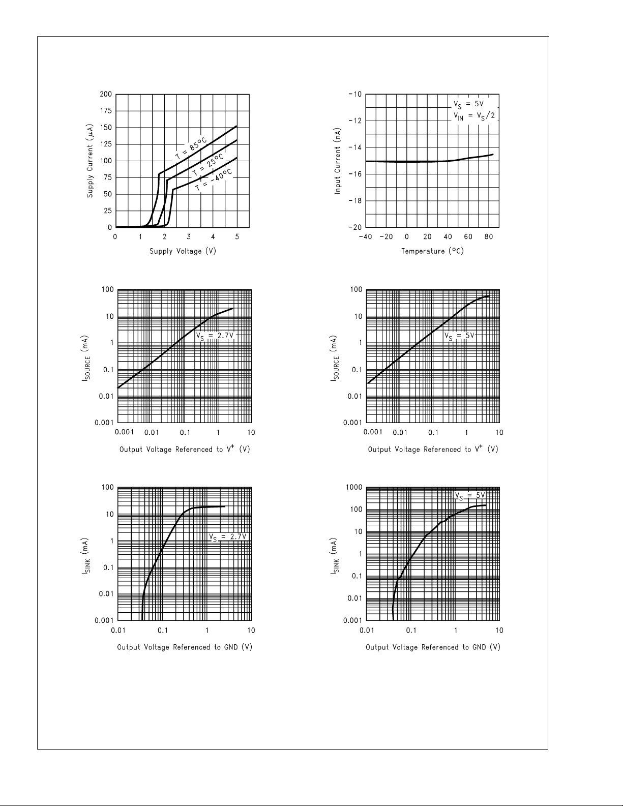
Typical Performance Characteristics Unless otherwise specified, V
= 25˚C.
T
A
= +5V, single supply,
S
Supply Current vs. Supply Voltage (LMV321) Input Current vs. Temperature
10006073
Sourcing Current vs. Output Voltage Sourcing Current vs. Output Voltage
100060A9
10006069 10006068
Sinking Current vs. Output Voltage Sinking Current vs. Output Voltage
10006070 10006071
www.national.com5
Page 6
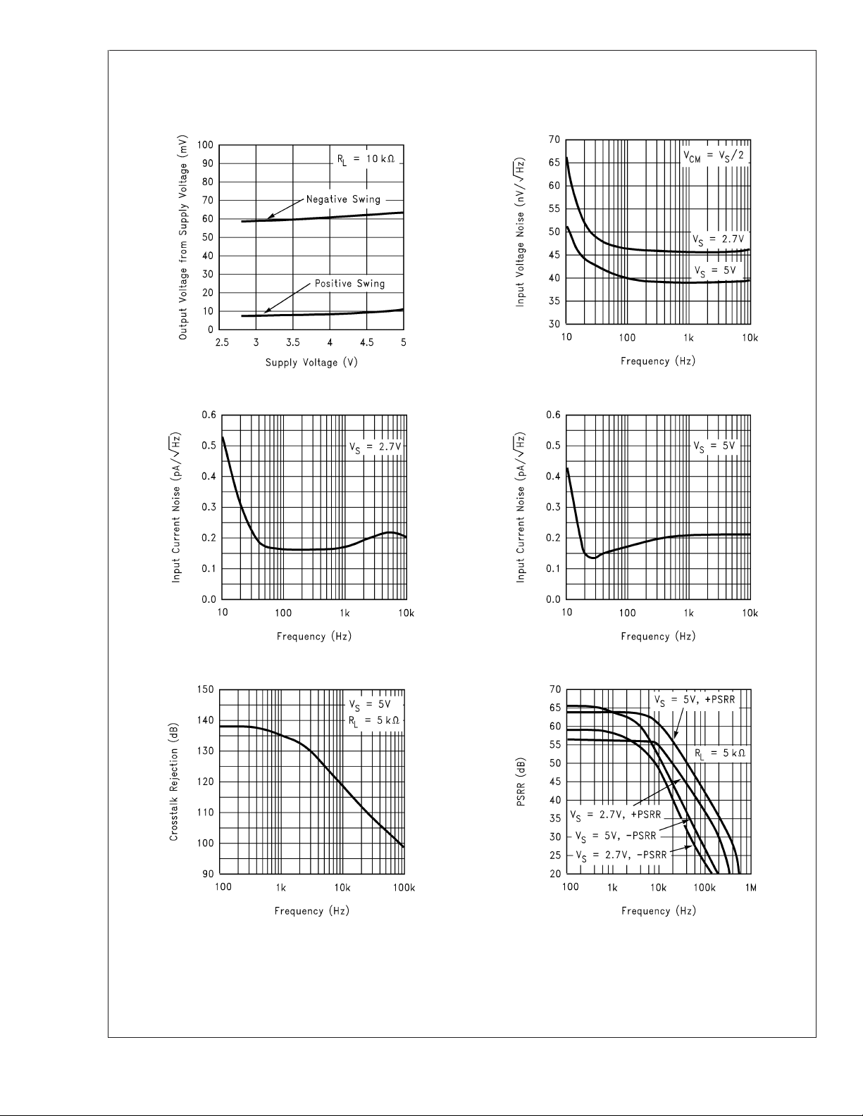
Typical Performance Characteristics Unless otherwise specified, V
= 25˚C. (Continued)
T
A
Output Voltage Swing vs. Supply Voltage Input Voltage Noise vs. Frequency
LMV321/LMV358/LMV324 Single/Dual/Quad
= +5V, single supply,
S
10006067
Input Current Noise vs. Frequency Input Current Noise vs. Frequency
10006060 10006058
Crosstalk Rejection vs. Frequency PSRR vs. Frequency
10006056
10006061
www.national.com 6
10006051
Page 7
LMV321/LMV358/LMV324 Single/Dual/Quad
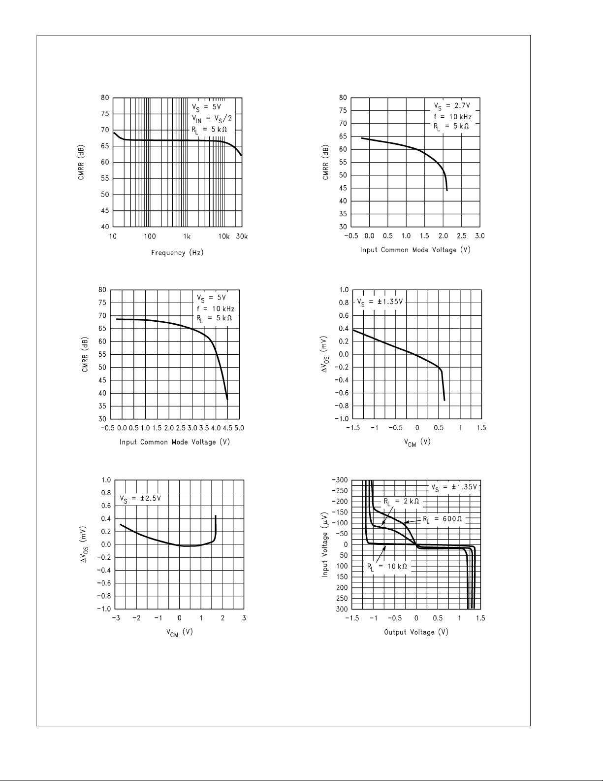
Typical Performance Characteristics Unless otherwise specified, V
= 25˚C. (Continued)
T
A
CMRR vs. Frequency CMRR vs. Input Common Mode Voltage
10006062
CMRR vs. Input Common Mode Voltage ∆VOSvs. CMR
= +5V, single supply,
S
10006064
10006063
∆VOSvs. CMR Input Voltage vs. Output Voltage
10006050
10006053
10006054
www.national.com7
Page 8
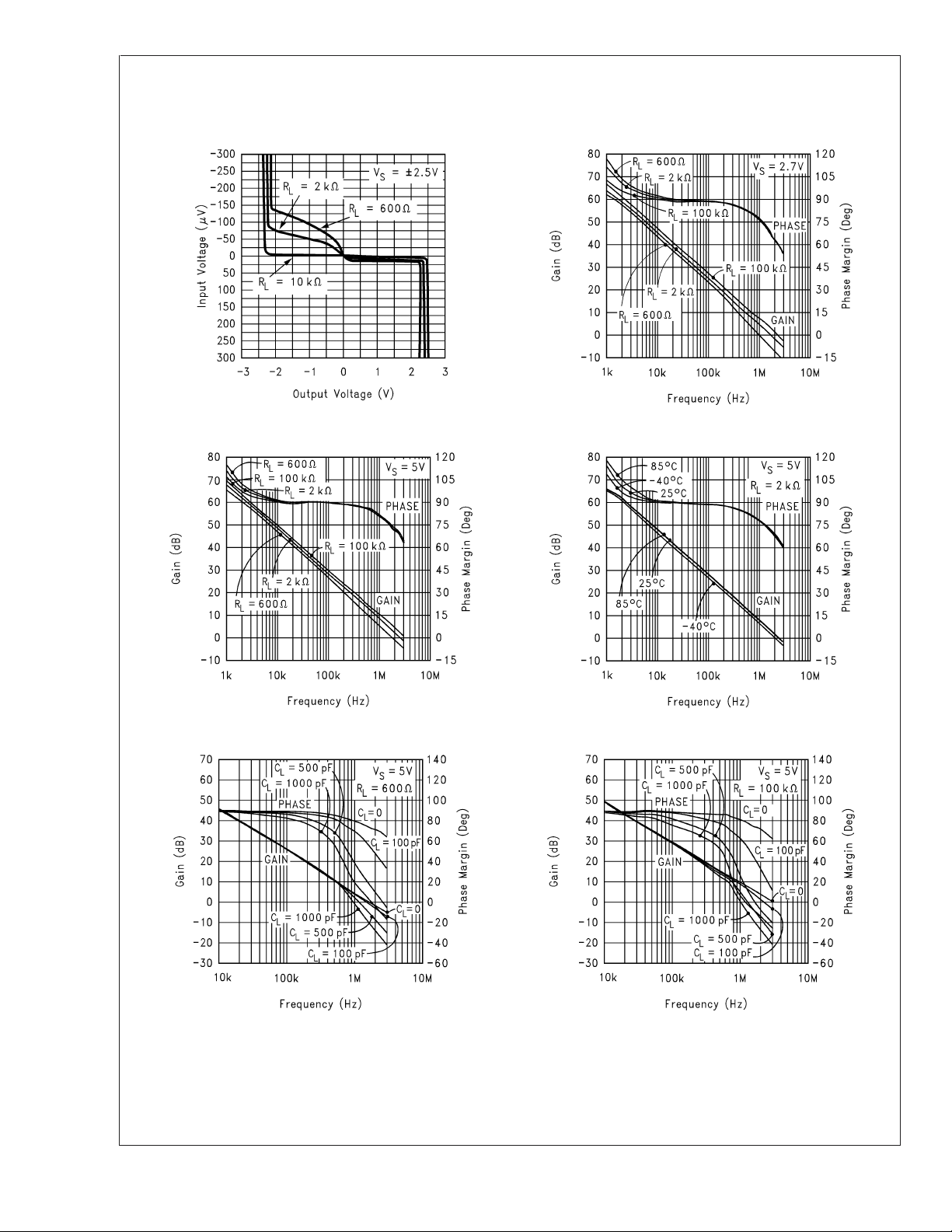
Typical Performance Characteristics Unless otherwise specified, V
= 25˚C. (Continued)
T
A
Input Voltage vs. Output Voltage Open Loop Frequency Response
LMV321/LMV358/LMV324 Single/Dual/Quad
= +5V, single supply,
S
10006052
10006042
Open Loop Frequency Response Open Loop Frequency Response vs. Temperature
10006041
10006043
Gain and Phase vs. Capacitive Load Gain and Phase vs. Capacitive Load
10006045 10006044
www.national.com 8
Page 9
LMV321/LMV358/LMV324 Single/Dual/Quad
Typical Performance Characteristics Unless otherwise specified, V
= 25˚C. (Continued)
T
A
= +5V, single supply,
S
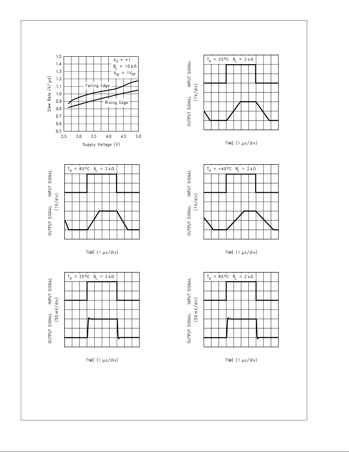
Slew Rate vs. Supply Voltage Non-Inverting Large Signal Pulse Response
10006057
Non-Inverting Large Signal Pulse Response Non-Inverting Large Signal Pulse Response
10006088
100060A1 100060A0
Non-Inverting Small Signal Pulse Response Non-Inverting Small Signal Pulse Response
10006089 100060A2
www.national.com9
Page 10

Typical Performance Characteristics Unless otherwise specified, V
= 25˚C. (Continued)
T
A
Non-Inverting Small Signal Pulse Response Inverting Large Signal Pulse Response
LMV321/LMV358/LMV324 Single/Dual/Quad
100060A3 10006090
Inverting Large Signal Pulse Response Inverting Large Signal Pulse Response
= +5V, single supply,
S
100060A4 100060A5
Inverting Small Signal Pulse Response Inverting Small Signal Pulse Response
10006091 100060A6
www.national.com 10
Page 11

LMV321/LMV358/LMV324 Single/Dual/Quad
Typical Performance Characteristics Unless otherwise specified, V
= 25˚C. (Continued)
T
A
Inverting Small Signal Pulse Response Stability vs. Capacitive Load
100060A7
Stability vs. Capacitive Load Stability vs. Capacitive Load
= +5V, single supply,
S
10006046
10006047
Stability vs. Capacitive Load THD vs. Frequency
10006048
10006049
10006059
www.national.com11
Page 12

Typical Performance Characteristics Unless otherwise specified, V
= 25˚C. (Continued)
T
A
Open Loop Output Impedance vs. Frequency Short Circuit Current vs. Temperature (Sinking)
LMV321/LMV358/LMV324 Single/Dual/Quad
= +5V, single supply,
S
10006055
Short Circuit Current vs. Temperature (Sourcing)
10006066
10006065
www.national.com 12
Page 13

Application Notes
1.0 BENEFITS OF THE LMV321/358/324
Size: The small footprints of the LMV321/358/324 packages
save space on printed circuit boards, and enable the design
of smaller electronic products, such as cellular phones, pagers, or other portable systems. The low profile of the
LMV321/358/324 make them possible to use in PCMCIA
type III cards.
Signal Integrity
Signals can pick up noise between the signal source and the
amplifier. By using a physically smaller amplifier package,
the LMV321/358/324 can be placed closer to the signal
source, reducing noise pickup and increasing signal integrity.
Simplified Board Layout
These products help you to avoid using long pc traces in
your pc board layout. This means that no additional components, such as capacitors and resistors, are needed to filter
out the unwanted signals due to the interference between
the long pc traces.
Low Supply Current
These devices will help you to maximize battery life. They
are ideal for battery powered systems.
LMV321/LMV358/LMV324 Single/Dual/Quad
Output Voltage (500mV/div)
Time (50µs/div)
10006097
FIGURE 1. Output Swing of LMV324
Low Supply Voltage
National provides guaranteed performance at 2.7V and 5V.
These guarantees ensure operation throughout the battery
lifetime.
Rail-to-Rail Output
Rail-to-rail output swing provides maximum possible dynamic range at the output. This is particularly important
when operating on low supply voltages.
Input Includes Ground
Allows direct sensing near GND in single supply operation.
+
The differential input voltage may be larger than V
without
damaging the device. Protection should be provided to prevent the input voltages from going negative more than −0.3V
(at 25˚C). An input clamp diode with a resistor to the IC input
terminal can be used.
Ease Of Use & Crossover Distortion
The LMV321/358/324 offer specifications similar to the familiar LM324. In addition, the new LMV321/358/324 effectively eliminate the output crossover distortion. The scope
photos in Figure 1 and Figure 2 compare the output swing of
the LMV324 and the LM324 in a voltage follower configuration, with V
=±2.5V and RL(= 2kΩ) connected to GND. It
S
is apparent that the crossover distortion has been eliminated
in the new LMV324.
Output Voltage (500mV/div)
Time (50µs/div)
10006098
FIGURE 2. Output Swing of LM324
2.0 CAPACITIVE LOAD TOLERANCE
The LMV321/358/324 can directly drive 200pF in unity-gain
without oscillation. The unity-gain follower is the most sensitive configuration to capacitive loading. Direct capacitive
loading reduces the phase margin of amplifiers. The combination of the amplifier’s output impedance and the capacitive
load induces phase lag. This results in either an underdamped pulse response or oscillation. To drive a heavier
capacitive load, circuit in Figure 3 can be used.
10006004
FIGURE 3. Indirectly Driving A Capacitive Load Using
Resistive Isolation
www.national.com13
Page 14

Application Notes (Continued)
In Figure 3 , the isolation resistor R
form a pole to increase stability by adding more phase
C
L
margin to the overall system. The desired performance depends on the value of R
value, the more stable V
. The bigger the R
ISO
OUT
waveform of Figure 3 using 620Ω for R
(1v/div)
LMV321/LMV358/LMV324 Single/Dual/Quad
and the load capacitor
ISO
will be. Figure 4 is an output
and 510pF for CL..
ISO
ISO
input bias current will be reduced. The circuit in Figure 6
shows how to cancel the error caused by input bias current.
resistor
10006006
FIGURE 6. Cancelling the Error Caused by Input Bias
Current
4.0 TYPICAL SINGLE-SUPPLY APPLICATION CIRCUITS
Output Signal Input Signal
Time (2µs/div)
10006099
FIGURE 4. Pulse Response of the LMV324 Circuit in
Figure 3
The circuit in Figure 5 is an improvement to the one in Figure
3 because it provides DC accuracy as well as AC stability. If
there were a load resistor in Figure 3, the output would be
voltage divided by R
Figure 5,R
provides the DC accuracy by using feed-
F
forward techniques to connect V
in choosing the value of R
the LMV321/358/324. C
and the load resistor. Instead, in
ISO
to RL. Caution is needed
IN
due to the input bias current of
F
and R
F
serve to counteract the
ISO
loss of phase margin by feeding the high frequency component of the output signal back to the amplifier’s inverting
input, thereby preserving phase margin in the overall feedback loop. Increased capacitive drive is possible by increasing the value of C
. This in turn will slow down the pulse
F
response.
4.1 Difference Amplifier
The difference amplifier allows the subtraction of two voltages or, as a special case, the cancellation of a signal
common to two inputs. It is useful as a computational amplifier, in making a differential to single-ended conversion or in
rejecting a common mode signal.
10006007
10006019
FIGURE 7. Difference Amplifier
10006005
FIGURE 5. Indirectly Driving A Capacitive Load with
DC Accuracy
3.0 INPUT BIAS CURRENT CANCELLATION
The LMV321/358/324 family has a bipolar input stage. The
typical input bias current of LMV321/358/324 is 15nA with 5V
supply. Thus a 100kΩ input resistor will cause 1.5mV of error
voltage. By balancing the resistor values at both inverting
and non-inverting inputs, the error caused by the amplifier’s
www.national.com 14
4.2 Instrumentation Circuits
The input impedance of the previous difference amplifier is
set by the resistors R
1,R2,R3
, and R4. To eliminate the
problems of low input impedance, one way is to use a
voltage follower ahead of each input as shown in the following two instrumentation amplifiers.
Page 15

Application Notes (Continued)
4.2.1 Three-Op-Amp Instrumentation Amplifier
The quad LMV324 can be used to build a three-op-amp
instrumentation amplifier as shown in Figure 8.
10006085
FIGURE 8. Three-op-amp Instrumentation Amplifier
The first stage of this instrumentation amplifier is a
differential-input, differential-output amplifier, with two voltage followers. These two voltage followers assure that the
input impedance is over 100 MΩ. The gain of this instrumentation amplifier is set by the ratio of R2/R1. R
, and R4equal R2. Matching of R3to R1and R4to R
R
1
affects the CMRR. For good CMRR over temperature, low
drift resistors should be used. Making R
than R
between R
and adding a trim pot equal to twice the difference
2
and R4will allow the CMRR to be adjusted for
2
optimum.
4.2.2 Two-op-amp Instrumentation Amplifier
A two-op-amp instrumentation amplifier can also be used to
make a high-input-impedance dc differential amplifier (Fig-
ure 9) . As in the three-op-amp circuit, this instrumentation
amplifier requires precise resistor matching for good CMRR.
should equal to R1and R3 should equal R2.
R
4
should equal
3
slightly smaller
4
LMV321/LMV358/LMV324 Single/Dual/Quad
4.3 Single-Supply Inverting Amplifier
There may be cases where the input signal going into the
amplifier is negative. Because the amplifier is operating in
single supply voltage, a voltage divider using R
implemented to bias the amplifier so the input signal is within
the input common-mode voltage range of the amplifier. The
capacitor C
tor R
1
. The values of R1and C1affect the cutoff frequency, fc =
V
IN
1/2πR
As a result, the output signal is centered around mid-supply
(if the voltage divider provides V
is placed between the inverting input and resis-
1
to block the DC signal going into the AC signal source,
.
1C1
+
/2 at the non-inverting
input). The output can swing to both rails, maximizing the
signal-to-noise ratio in a low voltage system.
2
10006020
FIGURE 10. Single-Supply Inverting Amplifier
4.4 ACTIVE FILTER
4.4.1 Simple Low-Pass Active Filter
The simple low-pass filter is shown in Figure 11. Its lowfrequency gain (ω→0) is defined by -R
low-frequency gains other than unity to be obtained. The
filter has a -20dB/decade roll-off after its corner frequency fc.
should be chosen equal to the parallel combination of R
R
2
and R3to minimize errors due to bias current. The frequency
response of the filter is shown in Figure 12.
3
10006013
. This allows
3/R1
and R4is
1
10006011
10006035
FIGURE 9. Two-Op-amp Instrumentation Amplifier
www.national.com15
Page 16

Application Notes (Continued)
LMV321/LMV358/LMV324 Single/Dual/Quad
FIGURE 11. Simple Low-Pass Active Filter
10006037
10006014
Its transfer function is
(2)
10006016
FIGURE 13. Sallen-Key 2nd-Order Active Low-Pass
Filter
The following paragraphs explain how to select values for
R
1,R2,R3,R4,C1
, Q, and fc.
as A
LP
, and C2for given filter requirements, such
The standard form for a 2nd-order low pass filter is
10006015
FIGURE 12. Frequency Response of Simple Low-Pass
Active Filter in Figure 11
Note that the single-op-amp active filters are used in to the
applications that require low quality factor, Q( ≤ 10), low
frequency (≤ 5 kHz), and low gain (≤ 10), or a small value for
the product of gain times Q (≤ 100). The op amp should have
an open loop voltage gain at the highest frequency of interest at least 50 times larger than the gain of the filter at this
frequency. In addition, the selected op amp should have a
slew rate that meets the following requirement:
)x10−6V/µsec
HVOPP
opp
is the
where ω
Slew Rate ≥ 0.5x(ω
is the highest frequency of interest, and V
H
output peak-to-peak voltage.
4.4.2 Sallen-Key 2nd-Order Active Low-Pass Filter
The Sallen-Key 2nd-order active low-pass filter is illustrated
in Figure 13. The dc gain of the filter is expressed as
(3)
where
Q: Pole Quality Factor
: Corner Frequency
ω
C
Comparison between the Equation (2) and Equation (3)
yields
(4)
(5)
To reduce the required calculations in filter design, it is
convenient to introduce normalization into the components
and design parameters. To normalize, let ω
and C
1=C2=Cn
= 1F, and substitute these values into
= ωn= 1rad/s,
C
Equation (4) and Equation (5). From Equation (4), we obtain
(6)
From Equation (5), we obtain
(1)
www.national.com 16
(7)
Page 17

Application Notes (Continued)
For minimum dc offset, V
inverting and non-inverting inputs should be equal, which
means
From Equation (1) and Equation (8), we obtain
The values of C
1
As a design example:
Require: A
=2,Q=1,fc=1KHz
LP
Start by selecting C
is close to
+=V−
, the resistor values at both
(10)
and C2are normally close to or equal to
and C2. Choose a standard value that
1
(8)
(9)
An adjustment to the scaling may be made in order to have
realistic values for resistors and capacitors. The actual value
used for each component is shown in the circuit.
4.4.3 2nd-order High Pass Filter
A 2nd-order high pass filter can be built by simply interchanging those frequency selective components (R
) in the Sallen-Key 2nd-order active low pass filter. As
C
1,C2
1,R2
shown in Figure 14, resistors become capacitors, and capacitors become resistors. The resulted high pass filter has
the same corner frequency and the same maximum gain as
the previous 2nd-order low pass filter if the same components are chosen.
LMV321/LMV358/LMV324 Single/Dual/Quad
,
From Equations (6), (7), (9), (10),
R
=1Ω
1
=1Ω
R
2
=4Ω
R
3
=4Ω
R
4
The above resistor values are normalized values with ω
1rad/s and C
1=C2=Cn
= 1F. To scale the normalized cut-off
n
frequency and resistances to the real values, two scaling
factors are introduced, frequency scaling factor (k
pedance scaling factor (k
).
m
) and im-
f
Scaled values:
2=R1
3=R4
1=C2
= 15.9 kΩ
= 63.6 kΩ
= 0.01 µF
R
R
C
10006083
FIGURE 14. Sallen-Key 2nd-Order Active High-Pass
Filter
4.4.4 State Variable Filter
A state variable filter requires three op amps. One convenient way to build state variable filters is with a quad op amp,
such as the LMV324 (Figure 15).
=
This circuit can simultaneously represent a low-pass filter,
high-pass filter, and bandpass filter at three different outputs.
The equations for these functions are listed below. It is also
called "Bi-Quad" active filter as it can produce a transfer
function which is quadratic in both numerator and
denominator.
www.national.com17
Page 18

Application Notes (Continued)
LMV321/LMV358/LMV324 Single/Dual/Quad
where for all three filters,
FIGURE 15. State Variable Active Filter
A design example for a bandpass filter is shown below:
Assume the system design requires a bandpass filter with f
= 1kHz and Q = 50. What needs to be calculated are
capacitor and resistor values.
First choose convenient values for C
Then from Equation (11),
From Equation (12),
2R
= 1200pF
C
1
2=R1
= 30kΩ
1,R1
10006039
O
and R2:
(11)
(12)
www.national.com 18
From the above calculated values, the midband gain is H0=
= 100 (40dB). The nearest 5% standard values have
R
3/R2
been added to Figure 15.
4.5 PULSE GENERATORS AND OSCILLATORS
A pulse generator is shown in Figure 16. Two diodes have
been used to separate the charge and discharge paths to
capacitor C.
Page 19
Application Notes (Continued)
10006081
FIGURE 16. Pulse Generator
When the output voltage V
capacitor C is charged toward V
across C rises exponentially with a time constant τ =R
and this voltage is applied to the inverting input of the op
amp. Meanwhile, the voltage at the non-inverting input is set
at the positive threshold voltage (V
capacitor voltage continually increases until it reaches V
at which point the output of the generator will switch to its
low, V
(= 0V in this case). The voltage at the non-inverting
OL
input is switched to the negative threshold voltage (V
the generator. The capacitor then starts to discharge toward
exponentially through R1, with a time constant τ =R1C.
V
OL
When the capacitor voltage reaches V
pulse generator switches to V
charge, and the cycle repeats itself.
is first at its high, VOH, the
O
through R2. The voltage
OH
) of the generator. The
TH+
, the output of the
TH-
. The capacitor starts to
OH
TH-
2
TH+
)of
C,
LMV321/LMV358/LMV324 Single/Dual/Quad
10006086
FIGURE 17. Waveforms of the Circuit in Figure 16
As shown in the waveforms in Figure 17, the pulse width (T
is set by R
,
set by R
have different frequencies and pulse width by selecting dif-
, C and VOH, and the time between pulses (T2)is
2
, C and VOL. This pulse generator can be made to
1
ferent capacitor value and resistor values.
Figure 18 shows another pulse generator, with separate
charge and discharge paths. The capacitor is charged
through R
and is discharged through R2.
1
)
1
10006077
FIGURE 18. Pulse Generator
Figure 19 is a squarewave generator with the same path for
charging and discharging the capacitor.
www.national.com19
Page 20

Application Notes (Continued)
4.6.2 High Compliance Current Sink
A current sink circuit is shown in Figure 21. The circuit
requires only one resistor (R
) and supplies an output cur-
E
rent which is directly proportional to this resistor value.
LMV321/LMV358/LMV324 Single/Dual/Quad
FIGURE 19. Squarewave Generator
4.6 CURRENT SOURCE AND SINK
The LMV321/358/324 can be used in feedback loops which
regulate the current in external PNP transistors to provide
current sources or in external NPN transistors to provide
current sinks.
4.6.1 Fixed Current Source
A multiple fixed current source is show in Figure 20.A
voltage (V
voltage divider (R
cause the voltage drop across R
controls the emitter current of transistor Q
the base current of Q
is available out of the collector of Q
Large input resistors can be used to reduce current loss and
a Darlington connection can be used to reduce errors due to
the β of Q
The resistor, R
either above or below the 1mA reference value.
Q
2
= 2V) is established across resistor R3by the
REF
1
.
and R4). Negative feedback is used to
3
and Q2, essentially this same current
1
, can be used to scale the collector current of
2
to be equal to V
1
1
.
1
and if we neglect
10006076
REF
10006082
FIGURE 21. High Compliance Current Sink
4.7 POWER AMPLIFIER
A power amplifier is illustrated in Figure 22. This circuit can
provide a higher output current because a transistor follower
is added to the output of the op amp.
. This
10006079
FIGURE 22. Power Amplifier
10006080
FIGURE 20. Fixed Current Source
www.national.com 20
4.8 LED DRIVER
The LMV321/358/324 can be used to drive an LED as shown
in Figure 23.
10006084
FIGURE 23. LED Driver
Page 21

Application Notes (Continued)
4.9 COMPARATOR WITH HYSTERESIS
The LMV321/358/324 can be used as a low power comparator. Figure 24 shows a comparator with hysteresis. The
hysteresis is determined by the ratio of the two resistors.
V
TH+=VREF
V
TH−=VREF
/(1+R1/R2)+VOH/(1+R2/R1)
/(1+R1/R2)+VOL/(1+R2/R1)
=(V
V
H
OH−VOL
)/(1+R2/R1)
where
V
: Positive Threshold Voltage
TH+
: Negative Threshold Voltage
V
TH−
: Output Voltage at High
V
OH
V
: Output Voltage at Low
OL
: Hysteresis Voltage
V
H
Since LMV321/358/324 have rail-to-rail output, the
(V
) equals to VS, which is the supply voltage.
OH−VOL
H=VS
/(1+R2/R1)
V
Connection Diagrams
5-Pin SC70-5/SOT23-5 8-Pin SO/MSOP 14-Pin SO/TSSOP
LMV321/LMV358/LMV324 Single/Dual/Quad
The differential voltage at the input of the op amp should not
exceed the specified absolute maximum ratings. For real
comparators that are much faster, we recommend you to use
National’s LMV331/393/339, which are single, dual and quad
general purpose comparators for low voltage operation.
10006078
FIGURE 24. Comparator with Hysteresis
Top View
10006001
Top View
10006002
10006003
Top View
Ordering Information
Temperature Range
Package
−40˚C to +85˚C
5-Pin SC70-5 LMV321M7 A12 1k Units Tape and Reel MAA05
LMV321M7X A12 3k Units Tape and Reel
5-Pin SOT23-5 LMV321M5 A13 1k Units Tape and Reel MA05B
LMV321M5X A13 3k Units Tape and Reel
8-Pin Small Outline LMV358M LMV358M Rails
LMV358MX LMV358M 2.5k Units Tape and Reel
8-Pin MSOP LMV358MM LMV358 1k Units Tape and Reel
LMV358MMX LMV358 3.5k Units Tape and Reel
14-Pin Small Outline LMV324M LMV324M Rails
LMV324MX LMV324M 2.5k Units Tape and Reel
14-Pin TSSOP LMV324MT LMV324MT Rails
LMV324MTX LMV324MT 2.5k Units Tape and Reel
Packaging Marking Transport Media NSC DrawingIndustrial
M08A
MUA08A
M14A
MTC14
www.national.com21
Page 22

SC70-5 Tape and Reel
Specification
LMV321/LMV358/LMV324 Single/Dual/Quad
SOT-23-5 Tape and Reel
Specification
100060B3
TAPE FORMAT
Tape Section
TAPE DIMENSIONS
#
Cavities Cavity Status Cover Tape Status
Leader 0 (min) Empty Sealed
(Start End) 75 (min) Empty Sealed
Carrier 3000 Filled Sealed
250 Filled Sealed
Trailer 125 (min) Empty Sealed
(Hub End) 0 (min) Empty Sealed
www.national.com 22
100060B1
Page 23
SOT-23-5 Tape and Reel Specification (Continued)
8 mm 0.130 0.124 0.130 0.126 0.138±0.002 0.055±0.004 0.157 0.315±0.012
(3.3) (3.15) (3.3) (3.2) (3.5
Tape Size DIM A DIM Ao DIM B DIM Bo DIM F DIM Ko DIM P1 DIM W
REEL DIMENSIONS
±
0.05) (1.4±0.11) (4) (8±0.3)
LMV321/LMV358/LMV324 Single/Dual/Quad
100060B2
8 mm 7.00 0.059 0.512 0.795 2.165 0.331 + 0.059/−0.000 0.567 W1+ 0.078/−0.039
330.00 1.50 13.00 20.20 55.00 8.40 + 1.50/−0.00 14.40 W1 + 2.00/−1.00
Tape Size A B C D N W1 W2 W3
www.national.com23
Page 24

Physical Dimensions inches (millimeters)
unless otherwise noted
LMV321/LMV358/LMV324 Single/Dual/Quad
5-Pin SC70-5
NS Package Number MAA05A
5-Pin SOT23-5
NS Package Number MA05B
www.national.com 24
Page 25

Physical Dimensions inches (millimeters) unless otherwise noted (Continued)
8-Pin SOIC
NS Package Number M08A
LMV321/LMV358/LMV324 Single/Dual/Quad
8-Pin MSOPNS Package Number MUA08A
www.national.com25
Page 26

Physical Dimensions inches (millimeters) unless otherwise noted (Continued)
LMV321/LMV358/LMV324 Single/Dual/Quad
14-Pin SOIC
NS Package Number M14A
14-Pin TSSOPNS Package Number MTC14
www.national.com 26
Page 27

Notes
LMV321/LMV358/LMV324 Single/Dual/Quad General Purpose, Low Voltage, Rail-to-Rail Output
Operational Amplifiers
LIFE SUPPORT POLICY
NATIONAL’S PRODUCTS ARE NOT AUTHORIZED FOR USE AS CRITICAL COMPONENTS IN LIFE SUPPORT
DEVICES OR SYSTEMS WITHOUT THE EXPRESS WRITTEN APPROVAL OF THE PRESIDENT AND GENERAL
COUNSEL OF NATIONAL SEMICONDUCTOR CORPORATION. As used herein:
1. Life support devices or systems are devices or
systems which, (a) are intended for surgical implant
into the body, or (b) support or sustain life, and
whose failure to perform when properly used in
accordance with instructions for use provided in the
2. A critical component is any component of a life
support device or system whose failure to perform
can be reasonably expected to cause the failure of
the life support device or system, or to affect its
safety or effectiveness.
labeling, can be reasonably expected to result in a
significant injury to the user.
National Semiconductor
Americas Customer
Support Center
Email: new.feedback@nsc.com
Tel: 1-800-272-9959
www.national.com
National does not assume any responsibility for use of any circuitry described, no circuit patent licenses are implied and National reserves the right at any time without notice to change said circuitry and specifications.
National Semiconductor
Europe Customer Support Center
Fax: +49 (0) 180-530 85 86
Email: europe.support@nsc.com
Deutsch Tel: +49 (0) 69 9508 6208
English Tel: +44 (0) 870 24 0 2171
Français Tel: +33 (0) 1 41 91 8790
National Semiconductor
Asia Pacific Customer
Support Center
Email: ap.support@nsc.com
National Semiconductor
Japan Customer Support Center
Fax: 81-3-5639-7507
Email: jpn.feedback@nsc.com
Tel: 81-3-5639-7560
 Loading...