

查询LMV248供应商
LMV248
Dual Band GSM Power Controller
LMV248 Dual Band GSM Power Controller
September 2001
General Description
The LMV248 RF power amplifier controller allows simple
implementation of transmit power control loops in GSM and
DCS/PCS and mobile phones. The LMV248 supports, GaAs
HBT and bipolar RF power amplifiers. The device operates
from a single supply of 2.5V to 5V. The LMV248 includes an
error amplifier with an input summing network, input and
output band switches, input filters, and output drivers. Analog input signals processed are:
– Coupler/detector voltages from GSM and PCN band
power amplifier outputs.
– Base band DAC ramp signal.
– Temperature compensation diode voltages.
– Pre-bias voltage for faster PA control.
Selection of the GSM or PCN output driver is made using the
GSM/PCN band select pin.
The On/OFF pin allows rapid power up or shutdown of the
device during Tx or Rx slots. In the off mode, both output
drivers are set low for PA shutdown. In the on mode, the
non-active driver will remain low for continued PAshutdown.
A single external capacitor/resistor combination is used to
adjust the closed loop frequency response.
The LMV248 replaces multiple discrete parts, reducing
board area and cost. The LLP leadless package minimizes
board footprint and permits flexible optimized PCB placement.
Features
n Multi-band cellular operation (example: GSM, PCN)
n Support of GaAs HBT and bipolar technology
n Shutdown mode for power save in Rx slot (0.15µA)
n Integrated ramp filter
n Built-in current source for biasing Schottky diodes
n Pre-biasing of PA control gate voltage (V
n GPRS compliant
n External loop compensation
n Detector diode temperature compensation
n Miniature packaging: LLP-16: 4mm x 4mm x 0.8mm
HOME
)
Applications
n GSM mobile phone
n TDMA RF control
n Wireless LAN
n PC and PDA modules
n GPS navigation modules
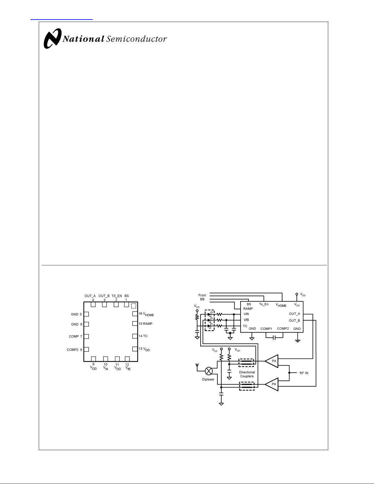
Connection Diagram
16-Pin LLP
Top View
Typical Application Circuit
10137201
10137202
FIGURE 1.
© 2001 National Semiconductor Corporation DS101372 www.national.com
Absolute Maximum Ratings (Note 1)
If Military/Aerospace specified devices are required,
LMV248
please contact the National Semiconductor Sales Office/
Distributors for availability and specifications.
Operating Temperature −40˚C
Storage Temperature Range −65˚C to 150˚C
Lead Temperature (solder, 4
sec) 260˚C
ESD Tolerance
Human Body Model (Note 1) 1500V
Machine Model 100V
Supply Voltage
V
to GND 5.5V
DD
Input Voltage Range
VfA, VfB, or TC to GND 10V
Ramp 0 to V
V
HOME
0toV
DD
DD
Junction Temperature 150˚C max
Operating Ratings (Note 1)
Supply Voltage
V
to GND 2.5V to 5V
DD
Input Voltage
VfA, VfB, or TC to V
Ramp 0.2V to 1.8V
V
HOME
Temperature Range −20˚C ≤ T
DD
DC and AC Electrical Characteristics
Unless otherwise specified, all limits guaranteed for VDD= 2.8V, GND = 0V, TJ= 25˚C. Boldface limits apply at temperature
range extremes of operating conditions.
Symbol Parameter Condition Min
(Note 7)
V
OUT
A, B
V
OUT
A, B
Positive Output Voltage Swing
A, B
Negative Output Voltage
Swing A, B
Sourcing 6mA, Tx_En = High
(Note 3)
Sinking 2mA,
= 0V 0.075 0.15 V
V
HOME
Tx_En = High
(Note 3,4,5)
V
OUT
A, B
V
OS
Negative Output Voltage
Swing A,B
Input Offset Voltage (Note 6) 60 80 100 mV
Sinking 2mA, TX_EN = Low
(Note 3,4,5)
BW Bandwidth (−3dB) Rf = 50k, No External Frequency
Compensation
SR Output Slew Rate No External Frequency
HOME
=0V
I
VHOME
I
BS
I
Tx_En
I
VfA
I
VfB
I
TC
Compensation, V
Current into V
Pin (Note 7)
HOME
Current into BS Pin (Note 7)
Current into En Pin (Note 7)
Forward Bias Current Sources (Note 7) 7 10 13 µA
Temperature Compensation
(Note 7) 7 10 13 µA
Current Source
I
Vf-TC
Match
Current Source Matching ITC/I
ITC/I
VfA
VfB
(Note 7)
V
LOW
BS or Tx_En Logic Low Input
(Note 7) 0.8 V
Level
V
HIGH
BS or Tx_En Logic High Input
(Note 7) 1.8 V
Level
I
SD
V
RD
t
d: Tx_En
Supply Current in Shutdown Tx_En = 0V 0.15
Vramp Deadband (Note 7) 160 200 mV
Output Delay: Tx_En to
Output
I
DD
V
A,B
OUT
Positive Supply Current V
OUT=VDD/2
(Note 6) 1.1 1.8 mA
Threshold Select Voltages Tx_En = High, V
(Note 3, 4, and 5)
HOME
=2V
2.6 2.7 V
3 5.5 V/µs
1.60 2 2.40 V
Typ
(Note 8)
Max
(Note 7)
0.06 0.15 V
>
1 MHz
<
<
<
±
2%
±
12%
<
3.5 6 µs
<
<
T
85˚C
J
0V to 5V
0V to 2V
≤ 85˚C
J
Units
5 µA
5 µA
5 µA
5 µA
www.national.com 2
DC and AC Electrical Characteristics (Continued)
Note 1: Absolute Maximum Ratings indicate limits beyond which damage to the device may occur. Operating Ratings indicate conditions for which the device is
intended to be functional, but specific performance is not guaranteed. For guaranteed specifications and the test conditions, see the Electrical Characteristics.
Note 2: Human Body Model (HBM) is 1.5kΩ in series with 100pF.
Note 3: The output is not short circuit protected internally. External protection is necessary to prevent overheating and destruction or adverse reliability.
Note 4: Transients and spikes during V
Note 5: No overshoot above100mVoccurs when Tx_En is switched high to low or low to high. The overshoot is influenced by the external compensation capacitor.
Note 6: Tested in closed loop configuration.
Note 7: All limits are guaranteed by design or statistical analysis.
Note 8: Typical values represent the most likely parametric norm.
on transition are allowed only as described in the diagram.
DD
Ordering Information
Package Part Number Packaging Marking Transport Media NSC
Drawing
16-Pin LLP
LMV248LQ LMV248 1k Units Tape and Reel
LMV248LQX LMV248 4.5k Units Tape and Reel
LQA16A
LMV248
www.national.com3
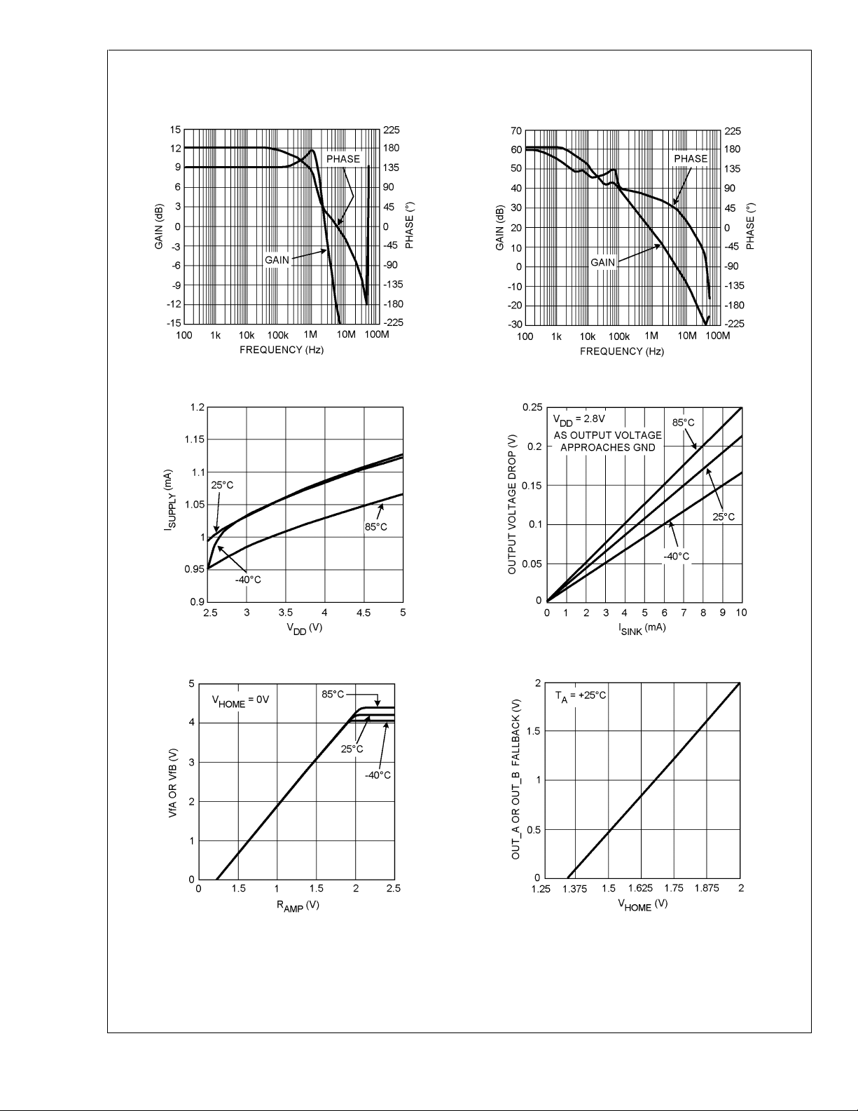
Typical Performance Characteristics
LMV248
Error Amp Closed Loop Gain and Phase
(Rf=R
= 137k, AV−2.8)
COMP
Error Amp Open Loop Gain and Phase
(Rf=R
= 137k, AV−2.8)
COMP
10137203
I
SUPPLY
vs. V
DD
10137205 10137206
Voltage Drop (Sinking)
VfA or VfB vs. Ramp Output Fallback Voltage Out A or Out B vs. V
10137204
HOME
10137207 10137208
www.national.com 4

Typical Performance
Characteristics
Voltage Drop (Sourcing)
(Continued)
Block Diagram
LMV248
10137209
FIGURE 2.
10137210
www.national.com5

Application Section
Pin Description
LMV248
See
Figure 1
for the basics of a typical LMV248 dual band
Figure 2
internal architecture
for a simplified block diagram of the LMV248’s
See
application.
TABLE 1.
Pin Name Description
Power Supply 5, 6 GND Power Ground; both pins must be tied together.
9,11, 13 V
DD
Digital Inputs 1 BS Selects the RF detector input (VfA or VfB) and the corresponding output
2 Tx_En A HIGH input enables the input and output amplifiers (VfA and Out_A or
Analog Inputs 10 VfA Detector diodes for the RF power detector are connected here. An
12 VfB
14 TC The reference diode used for temperature compensation of the VfA and
15 Ramp Sets the RF output power level. The useful input voltage range is from
16 V
HOME
Compensation 7 Comp1 Connect an external RC network here for overall loop compensation and
8 Comp2
Outputs 4 Out A A rail-to-rail output capable of sourcing is 6mA, sinking 2mA, with less
3 Out B
Note 9: All inputs and outputs are referenced to GND, except VfA, VfB, and TC, which are referenced to VDD.
Note 10: For the digital inputs, a LOW is ≤ 0.8V and HIGH is ≥ 1.8V.
Note 11: RF power detection is usually via a RF detector diode and a RF power coupler.
Positive Supply Voltage
amplifier (Out_A or Out_B) enabled when the Tx_En is HIGH. The
compensation is also connected to the correct amplifier automatically.
A HIGH input enables Out_A.
A LOW input enables Out_B.
The other unselected output is held close to GND.
VfB and Out_B) selected by the band select pin, BS.
internal switch connects a 10µA current sink to the input pin selected by
BS to bias the detector diode. This signal is referenced to V
DD
Notes 9 and 11).
VfB RF power signals is connected here. Internally, a 10µA current sink
connects to this pin to bias the reference diode. This signal is referenced
. (See notes 9 and 11).
to V
DD
0.2V to 1.8V, although voltages from 0V to V
are allowed. An internal
DD
filter with a corner frequency of approximately 1.6MHz smooths the
Ramp signal, to eliminate step discontinuities from the baseband DAC’s
output.
Sets the desired minimum output voltage of the controller (selected by
BS) to the threshold voltage of the RF power amplifier. This reduces
ramp up time, since a smaller voltage range is slewed across. The
recommended input voltage range is from 0V to 2V.
to control the closed loop frequency response. In most cases this
network will be simply a capacitor. Conventional loop stability techniques
can be used in selecting this network, such as Bode plots.
than 200mV drop including over temperature. The output is free from
glitches when enabled by Tx_En. When an output is not selected by BS,
it is close to GND. When Tx_En is low, output voltages are near GND.
. (See
www.national.com 6

Application Section (Continued)
The LMV248 as a RF Power Amplifier (PA) Controller
The LMV248, a member of National Semiconductor’s family
of RF power amplifier (PA) power controllers, is used to
regulate the RF transmit power in TDMA (GSM, EGSM,
PCN, PCS AND DCS) mobile phones. Capable of controlling
up to two RF output amplifiers and of triple band operation
(GSM, DCS, and PCS) the device supports both bipolar and
FET RF power amplifiers including Silicon BJT,CMOS, SiGe
HBT, and GaAs HBT.
Figure 1
application. The key components are:
•
•
•
•
•
The block diagram in
architecture. The LMV248 contains input filters and conditioning amplifiers, an input summing network, detector biasing current source, error amplifier, output band select function, and output drivers.
Power Supplies
The LMV248 supports a single supply with the battery voltage at V
Digital Input Signals:
The LMV248 has two digital control signals:
•
•
The band select pin, BS, selects which band (i.e which
output and input channel) is active. A high enables Out_A, a
low enables Out_B. The transmit enable pin, Tx_En, is used
to enable the BS selected output during transmit (Tx) slots
and disable the outputs during receive (Rx) slots. Disabling
the output during the receive (Rx) slot shuts down the
LMV248’s output stages and the RF power amplifiers, conserving battery power. A high input on the transmit enable
signal, Tx_En, brings the amplifier out of shutdown within
about 4µs. The output is glitch-free when enabled by this pin.
When an output is either not selected by BS or Tx_En is low,
its level is near GND. Internally, the band select pin, BS,
selects the correct input line and output amplifier,and places
the external compensation network across the active amplifier using analog switches.
Error Amplifier/Loop Compensation
The error amplifier (A1) controls the overall loop regulation
and response. Frequency compensation and stabilization of
the RF output power regulating loop is accomplished by a
capacitor (or resistor/capacitor network) across Comp1 and
Comp2 of the LMV248. This external network sets the
closed loop frequency response. In most cases this network
will simply be a capacitor. Conventional loop stability techniques can be used in selecting this network, such as Bode
plots.
Analog Inputs
At VfA and VfB are voltages proportional to the RF power
output of channel A and channel B respectively. Each of
these signals is derived from the RF output power via a RF
shows the basics of a typical LMV248 dual band
Two power amplifiers, usually for the GSM or DCS/PCS
bands.
RF directional couplers where two single or one dual
channel RF coupler could be used.
Up to three Schottky RF detector diodes, one for each
directional coupler output and one for temperature compensation.
A RF diplexer.
A dual or tri-band antenna.
Figure 2
.
DD
shows the LMV248’s internal
Transmit enable signal, Tx_En.
Band select signal, BS.
directional coupler a capacitor and a Schottky RF detector
diode. A single two-channel RF coupler could be used instead of the two single-channel RF couplers shown in
1
.
Figure
If only one input and output is needed, just connect BS high
or low and use the selected channel. At the TC input, a
reference diode identical to the detector diodes, and thermally coupled to them, is used for temperature compensation of the VfA and VfB signals.
VfA, VfB and TC are referenced to V
. A 10µA current sink
DD
internal to the LMV248 connects to the VfA, VfB and TC pins
to bias the diodes. The quiescent voltage on all three pins is
one diode drop below V
. The actual Ramp input value sets
DD
the RF output power. The recommended Ramp voltage
range for RF power control is 0.2V to 1.8V. The Ramp input
will tolerate voltages from 0V to V
without malfunction or
DD
damage. This signal usually comes from the baseband controller’s DAC (digital to analog converter), its shape being
defined by the relevant GSM, PCN, or DCS standard.
The Ramp input does not change the output level from the
idle level set by V
until the level reaches about 200mV,
HOME
so offset voltages in the DAC or amplifier supplying the
Ramp signal will not cause excess RF signal output and
increased power consumption. An internal RC filter with a
corner frequency of approximately 1.6MHz smooths the
Ramp signal, to eliminate step discontinuities at the baseband DAC’s output. Ramp is ground referenced, so supply
variations are rejected.
V
is used to set the output selected by BS to the
HOME
threshold voltage of the RF power amplifier. The variable
V
voltage level supports different PAShut off thresholds
HOME
as well as boost output voltage to minimize phase delay at
low power levels. The V
voltage can be derived from a
HOME
reference, resistive voltage divider, or DAC output. The recommended V
to 2V. The V
voltage range for threshold control is 0V
HOME
input will tolerate voltages from 0V to V
HOME
DD
without malfunction or damage. The minimum output voltage
at Out_A or Out_B set by V
V
HOME.VHOME
is ground referenced. V
is approximately 3.0 x
HOME
HOME
does not affect
the minimum voltage of the output not selected by BS.
For maximum performance a fine adjust is needed for
V
, since each individual RF power amplifier’s threshold
HOME
voltage is slightly different from the nominal datasheet value.
Analog Outputs
Outputs Out_A and Out_B are driven by rail-to-rail amplifiers
capable of both sourcing and sinking. Either output can
source 6mA and sink 2mA with less than 200mV voltage
drop over recommended operating conditions. The output is
free from glitches when enabled by Tx_En. When an output
is not selected by BS, its level is near GND.
Understanding the LMV248
Input Structure
The LMV248 simplified block diagram of
Figure 2
shows the
IC’s internal structure. Input VfA goes through a resistor
(approximately 48.5kΩ) and analog switch to the inverting
input of the error amplifier A1. Input VfB goes through a
different resistor (also approximately 48.5kΩ) and analog
switch to the inverting input of the error amplifier A1. These
two analog switches are controlled by BS. VfA is selected
when BS is high and VfB is selected when BS is low. The
temperature compensation signal, TC, goes through a series
resistance of about 48.5kΩ, to the non-inverting input of the
error amplifier A1. This way the relatively large static DC
offset of the input signal is mostly removed from the differential signal to be amplified by A1, and the temperature
LMV248
www.national.com7

Application Section (Continued)
dependency of the external detector diodes is cancelled.
LMV248
(Adding the temperature correction to the non-inverting terminal is identical to subtracting the temperature correction
from the inverting terminal). The 10µA current sinks connected to the signal paths for VfA, VfB, and TC provide a
bias current for the detector and temperature compensation
diodes. An approximate 200mV deadband for the Ramp
signal is preset.
Ramp Signal
The Ramp signal, which is positive going and ground referenced, is the reference for the closed loop RF output control.
The Ramp signal is smoothed by internal filter with a corner
frequency of approximately 1.6MHz, formed from a 20kΩ
resistor and 5pF capacitor. This filter eliminates step discontinuities at the baseband DAC’s output. Transconductance
amplifier A2 provides current sinking proportional to the
Ramp signal.
Since the output of A2 connects to the inverting terminal of
A1, A1 draws current from VfA or VfB through the 48.5kΩ
series resistance previously mentioned. This reduces the
voltage seen at the inverting terminal by the voltage drop
across the 48.5kΩ series resistance. The transconductance
of A2 is 1/(20kΩ). The net differential signal between the
non-inverting and inverting terminals of the error amplifier is
2.42 x Ramp-(Vf-TC). This means that the average (Vf-TC)
will be regulated to 2.42 x Ramp and that we want to choose
the RF directional coupler so that the peak RF detector
output at the maximum Ramp satisfies: (Peak Vf)-TC ≤ 2.42
x (maximum Ramp). See “Selecting Coupler/Detector” in the
next section. Note that the recommended maximum Ramp
≤ 2V.
V
HOME
Amplifier A3 and the diode D1 at its output clamp the low
value of the active output to the value set by V
ever the outputs are enabled by Tx_En. V
the inverting input of amplifier A3. The non-inverting input of
amplifier A3 connects to the active output selected by BS,
selection being done by analog switches. Also connecting to
the non-inverting input of amplifier A3 is a voltage divider.
This makes the equation for the minimum output voltage 3.0
xV
HOME
.
Outputs
The output amplifiers A4 and A5 are rail-to-rail complementary MOS output stages using Class AB control, and capable
of both sourcing and sinking current. The output amplifier not
selected by BS is disabled; both output amplifiers are disabled when Tx_En is low. This conserves power.
The single compensation/stabilization network across
Comp1 and Comp2 is switched across the correct output
amplifier by analog switches controlled by BS.
HOME
, when-
HOME
connects to
Typical LMV248 Configurations:
10137211
FIGURE 3. One Input, One Output (A)
10137212
FIGURE 4. One Input, One Output (B)
www.national.com 8
10137213
FIGURE 5. One Input, Two Outputs

Application Section (Continued)
The LMV248 has separate inputs for the coupler/detector
feedback signal(s). These may be combined as a single
input when using a single coupler/detector that accommodates both RF bands. When the two are combined as shown
in
Figure 5
maintain correct temperature compensation characteristics
for the applications circuit, an external biasing resistor, R'
should be added externally. For this arrangement, VfA, VfB,
and TC all are returned to a common supply, V
Selecting Coupler/Detector
Coupler Calculations:
The applied Ramp voltage controls the RF power output.
Because of this the maximum Ramp voltage sets the minimum attenuation that is allowed in the direction coupler used
to sense output power.
The basic equation is;
For peak detection it is;
The coupling factor, at maximum power, is defined as C
or,
Cf=(V
peak power
The limit conditions for the maximum ramp and max power
out is,
internal current sources are placed in parallel. To
.
CC
2
/R
O
xRO) for couplers that sense
rampmax
)2/2x(P
P
O=Vrms
outmax
f
= 2.0V
= 2Watts
=50Ω
= 10 x log10[(1/2)(V
= −16.98dB
rampmax
)2/P
outmaxxRO
)]
C
C
V
P
R
fdB
fdB
rampmax
outmax
O
Attenuation in the directional coupler should be at least
−17dB, to assure maximum power out.
General Device Equations
Calculation:
Let Vf be VfA or VfB as selected by BS. Let RVf be the
external series resistance from Vf to the Detector diode.
Voltage at the non-inverting terminal of A1 V
= TC, since
NI
current into A2’s input is small.
Voltage at the inverting terminal of A1 V
INV
=Vf-
[Ramp/(20kΩ)] x (RVf + 48.5kΩ)
Assuming the external series resistance for VfA and VfB is
<<
48.5kΩ:
Voltage at the inverting terminal of A1 V
= Vf – 2.42 x
INV
Ramp
Differential voltage at A1 inputs = V
NI-VINV
= TC - (Vf - 2.42
x Ramp) = 2.42 x Ramp - (Vf - TC).
Closed loop regulation of RF output power will force the
average differential voltage at A1 inputs to approach zero:
Average
Including the V
the equation for the VfA, B vs. V
VfA, B = 2.42 x (V
deadband and the device offset voltage,
ramp
-200mV) + TC - 80mV, all variables
ramp
relationship becomes:
ramp
being ground referenced DC voltages.
LMV248
www.national.com9

Application Section (Continued)
LMV248
Timing Diagram
Time Slot Enabled
#
1
Timing Diagram#2
Tx/Rx Enabled
10137216
www.national.com 10
10137217

Physical Dimensions inches (millimeters)
unless otherwise noted
LMV248 Dual Band GSM Power Controller
NS Product Number LQA16A
LIFE SUPPORT POLICY
NATIONAL’S PRODUCTS ARE NOT AUTHORIZED FOR USE AS CRITICAL COMPONENTS IN LIFE SUPPORT
DEVICES OR SYSTEMS WITHOUT THE EXPRESS WRITTEN APPROVAL OF THE PRESIDENT AND GENERAL
COUNSEL OF NATIONAL SEMICONDUCTOR CORPORATION. As used herein:
1. Life support devices or systems are devices or
systems which, (a) are intended for surgical implant
into the body, or (b) support or sustain life, and
whose failure to perform when properly used in
accordance with instructions for use provided in the
2. A critical component is any component of a life
support device or system whose failure to perform
can be reasonably expected to cause the failure of
the life support device or system, or to affect its
safety or effectiveness.
labeling, can be reasonably expected to result in a
significant injury to the user.
National Semiconductor
Corporation
Americas
Email: support@nsc.com
www.national.com
National Semiconductor
Europe
Fax: +49 (0) 180-530 85 86
Email: europe.support@nsc.com
Deutsch Tel: +49 (0) 69 9508 6208
English Tel: +44 (0) 870 24 0 2171
Français Tel: +33 (0) 1 41 91 8790
National Semiconductor
Asia Pacific Customer
Response Group
Tel: 65-2544466
Fax: 65-2504466
Email: ap.support@nsc.com
National Semiconductor
Japan Ltd.
Tel: 81-3-5639-7560
Fax: 81-3-5639-7507
National does not assume any responsibility for use of any circuitry described, no circuit patent licenses are implied and National reserves the right at any time without notice to change said circuitry and specifications.
 Loading...