

查询LMV242供应商
LMV242
Dual Output, Quad-Band GSM/GPRS Power Amplifier
Controller
LMV242 Dual Output, Quad-Band GSM/GPRS Power Controller
July 2004
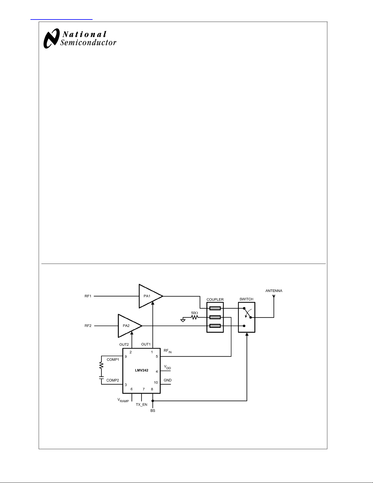
General Description
The LMV242 is a power amplifier (PA) controller intended for
use within an RF transmit power control loop in GSM/GPRS
mobile phones. The LMV242 supports all single-supply PA’s
including InGaP, HBT and bipolar power amplifiers. The
device operates with a single supply from 2.6V to 5.5V.
Included in the PA controller are an RF detector, a ramp filter
and two selectable output drivers that function as error amplifiers for two different bands. The LMV242 input interface
consists two analog and two digital inputs. The analog inputs
are the RF input, Ramp voltage input. The digital inputs
perform the function of “Band Select” and “Shutdown/
Transmit Enable” respectively. The “Band Select” function
enables either of two outputs, namely OUT1 when BS =
High, or output OUT2 when BS = Low. The output that is not
enabled is pulled low to the minimum output voltage. The
LMV242 is active in the case TX_EN = High. When TX_EN
= Low the device is in a low power consumption shutdown
mode. During shutdown both outputs will be pulled low to the
minimum output voltage. Individual PA characteristics are
accommodated by a user selectable external RC combination.
The LMV242 is offered in fully tested die form as well as in a
10-lead LLP package and is therefore especially suitable for
small footprint PA module solutions.
Typical Application
Features
n Support of InGaP HBT, bipolar technology
n Quad-band operation
n Shutdown mode for power save in R
n Integrated ramp filter
n 50 dB RF detector
n GPRS compliant
n External loop compensation option
n Accurate temperature compensation
n LLP package 3x3 mm and fully tested die sales
slot
X
Applications
n GSM/GPRS/TDMA/TD_SCDMA mobile phone
n Pulse RF control
n Wireless LAN
n GSM/GPRS power amplifier module
n Transmit module
20079501
VIP®is a registered trademark of National Semiconductor Corporation.
© 2004 National Semiconductor Corporation DS200795 www.national.com
Absolute Maximum Ratings (Note 1)
If Military/Aerospace specified devices are required,
LMV242
please contact the National Semiconductor Sales Office/
Distributors for availability and specifications.
Supply Voltage
- GND 6.5V Max
V
DD
ESD Tolerance (Note 2)
Human Body Model 2 kV
Machine Model 200V
Storage Temperature Range −65˚C to 150˚C
Junction Temperature (Note 6) 150˚C Max
Mounting Temperature
Infrared or convection (20 sec) 235˚C
Operating Ratings (Note 1)
Supply Voltage 2.6V to 5.5V
Operating Temperature
Range −40˚C to +85˚C
V
Voltage Range 0V to 2V
RAMP
RF Frequency Range 450 MHz to 2 GHz
2.6V Electrical Characteristics Unless otherwise specified, all limits are guaranteed to T
= 2.6V. Boldface limits apply at temperature extremes (Note 4).
V
DD
= 25˚C.
J
Symbol Parameter Condition Min Typ Max Units
I
DD
Supply Current V
=(VDD- GND)/2 6.9 9
OUT
mA
12
0.2 30 µA
V
HIGH
V
LOW
T
ON
I
EN,IBS
In Shutdown (TX_EN = 0V)
=(VDD- GND)/2
V
OUT
Logic Level to Enable Power (Note 7) 1.8 V
Logic Level to Disable Power (Note 7) 0.8 V
Turn-on-Time from Shutdown 3.6 6 µs
Current into TX_EN and BS Pin 0.03 5 µA
RAMP Amplifier
V
RD
1/R
RAMP
I
OUT RAMP
V
Deadband 155 206 265 mV
RAMP
Transconductance (Note 8) 70 96 120 µA/V
Ramp Amplifier Output Current V
=2V 100 162 µA
RAMP
RF Input
P
IN
RF Input Power Range (Note 5) 20 kΩ // 68 pF between
COMP1
and V
COMP2
V
−50
0
−63
dBm
dBV
−13
@
Logarithmic Slope (Note 9)
Logarithmic Intercept (Note 9)
R
IN
DC Resistance (Note 8) 55.7 Ω
900 MHz, 20 kΩ // 68 pF
between V
@
1800 MHz, 20 kΩ // 68 pF
between V
@
1900 MHz, 20 kΩ // 68 pF
between V
@
2000 MHz, 20 kΩ // 68 pF
between V
@
900 MHz, 20 kΩ // 68 pF
between V
@
1800 MHz, 20 kΩ // 68 if
between V
@
1900 MHz, 20 kΩ // 68 pF
between V
@
2000 MHz, 20 kΩ // 68 pF
between V
COMP1
COMP1
COMP1
COMP1
COMP1
COMP1
COMP1
COMP1
and V
and V
and V
and V
and V
and V
and V
and V
COMP2
COMP2
COMP2
COMP2
COMP2
COMP2
COMP2
COMP2
−1.74
−1.62
−1.60
−1.59
–50.4
–52.3
–51.9
–52.3
µA/dB
dBm
Error Amplifier
GBW Gain-Bandwidth Product (Note 8) 5.1 MHz
www.national.com 2
LMV242
2.6V Electrical Characteristics Unless otherwise specified, all limits are guaranteed to T
= 2.6V. Boldface limits apply at temperature extremes (Note 4). (Continued)
V
DD
= 25˚C.
J
Symbol Parameter Condition Min Typ Max Units
V
O
Output Swing from Rail From Positive Rail, Sourcing,
=7mA
I
O
From Negative Rail Sinking,
=−7mA
I
O
I
O
e
n
Output Short Circuit Current
(Note 3)
Output Referred Noise f
Sourcing, VO= 2.4V 10 29.5
Sinking, V
MEASURE
= 0.2V 10 27.1
O.
= 10 KHz,
47 90
115
52 90
115
700 nV/
mV
mA
RF Input = 1800 MHz, -10
dBm, 20 kΩ // 68 pF between
COMP1
and V
COMP2,VOUT
, (Note 8)
RAMP
V
=1.4V, set by V
SR Slew Rate 2.1 4.4 V/µs
5.0V Electrical Characteristics Unless otherwise specified, all limits are guaranteed to T
= 5.0V. Boldface limits apply at temperature extremes (Note 4).
V
DD
= 25˚C.
J
Symbol Parameter Condition Min Typ Max Units
I
DD
Supply Current V
=(VDD- GND)/2 7.8 12
OUT
mA
15
0.4 30 µA
V
HIGH
V
LOW
T
ON
I
EN,IBS
In Shutdown (TX_EN = 0V)
=(VDD- GND)/2
V
OUT
Logic Level to Enable Power (Note 7) 1.8 V
Logic Level to Disable Power (Note 7) 0.8 V
Turn-on-Time from Shutdown 1.5 6 µs
Current into TX_EN and BS Pin 0.03 5 µA
RAMP Amplifier
V
RD
1/R
RAMP
I
OUT RAMP
V
Deadband 155 206 265 mV
RAMP
Transconductance (Note 8) 70 96 120 µA/V
Ramp Amplifier Output Current V
=2V 100 168 µA
RAMP
RF Input
P
IN
R
IN
RF Input Power Range
(Note 5)
Logarithmic Slope
(Note 9)
Logarithmic Intercept
(Note 9)
20 kΩ // 68 pF between
V
@
between V
@
between V
@
between V
@
between V
@
between V
@
between V
@
between V
@
between V
and V
COMP1
COMP2
900 MHz, 20 kΩ // 68 pF
and V
COMP1
1800 MHz, 20 kΩ // 68 pF
and V
COMP1
1900 MHz, 20 kΩ // 68 pF
and V
COMP1
2000 MHz, 20 kΩ // 68 pF
and V
COMP1
900 MHz, 20 kΩ // 68 pF
and V
COMP1
1800 MHz, 20 kΩ // 68 pF
and V
COMP1
1900 MHz, 20 kΩ // 68 pF
and V
COMP1
2000 MHz, 20 kΩ // 68 pF
and V
COMP1
COMP2
COMP2
COMP2
COMP2
COMP2
COMP2
COMP2
COMP2
−50
0
−63
−13
−1.79
–1.69
−1.67
–1.65
–50.2
–52.5
–52.5
–52.9
dBm
dBV
µA/dB
dBm
DC Resistance (Note 8) 55.7 Ω
www.national.com3
5.0V Electrical Characteristics Unless otherwise specified, all limits are guaranteed to T
= 5.0V. Boldface limits apply at temperature extremes (Note 4). (Continued)
V
DD
LMV242
= 25˚C.
J
Symbol Parameter Condition Min Typ Max Units
Error Amplifier
GBW Gain-Bandwidth Product (Note 8) 5.7 MHz
V
O
Output Swing from Rail From Positive Rail, Sourcing,
=7mA
I
O
From Negative Rail Sinking,
IO=−7mA
I
O
e
n
Output Short Circuit Current
(Note 3)
Output Referred Noise f
Sourcing, VO= 4.8V 15 31.5
Sinking, V
MEASURE
= 0.2V 15 31.5
O
= 10 kHz,
31 80
105
35 80
105
770 nV/
RF Input = 1800 MHz,
-10dBm, 20 kΩ // 68 pF
between V
= 1.4V, set by V
V
OUT
COMP1
and V
COMP2
RAMP
,
,
(Note 8)
SR Slew Rate 2.5 4.9 V/µs
Note 1: Absolute Maximum Ratings indicate limits beyond which damage to the device may occur. Operating Ratings indicate conditions for which the device is
intended to be functional, but specific performance is not guaranteed. For guaranteed specifications and the test conditions, see the Electrical Characteristics.
Note 2: Human body model: 1.5 kΩ in series with 100 pF.
Note 3: The output is not short circuit protected internally. External protection is necessary to prevent overheating and destruction or adverse reliability.
Note 4: Electrical Table values apply only for factory testing conditions at the temperature indicated. Factory testing conditions result in very limited self-heating of
the device such that T
Note 5: Power in dBV = dBm + 13 when the impedance is 50Ω.
Note 6: The maximum power dissipation is a function of T
(T
J(MAX)-TA
Note 7: All limits are guaranteed by design or statistical analysis.
Note 8: Typical values represent the most likely parametric norm.
Note 9: Slope and intercept are calculated from graphs "V
)/θJA. All numbers apply for packages soldered directly into a PC board.
. No guarantee of parametric performance is indicated in the electrical tables under conditions of internal self-heating where T
J=TA
, θJAand TA. The maximum allowable power dissipation at any ambient temperature is PD=
J(MAX)
vs. RF input power" where the current is obtained by division of the voltage by 20 kΩ.
OUT
mV
mA
J
>
TA.
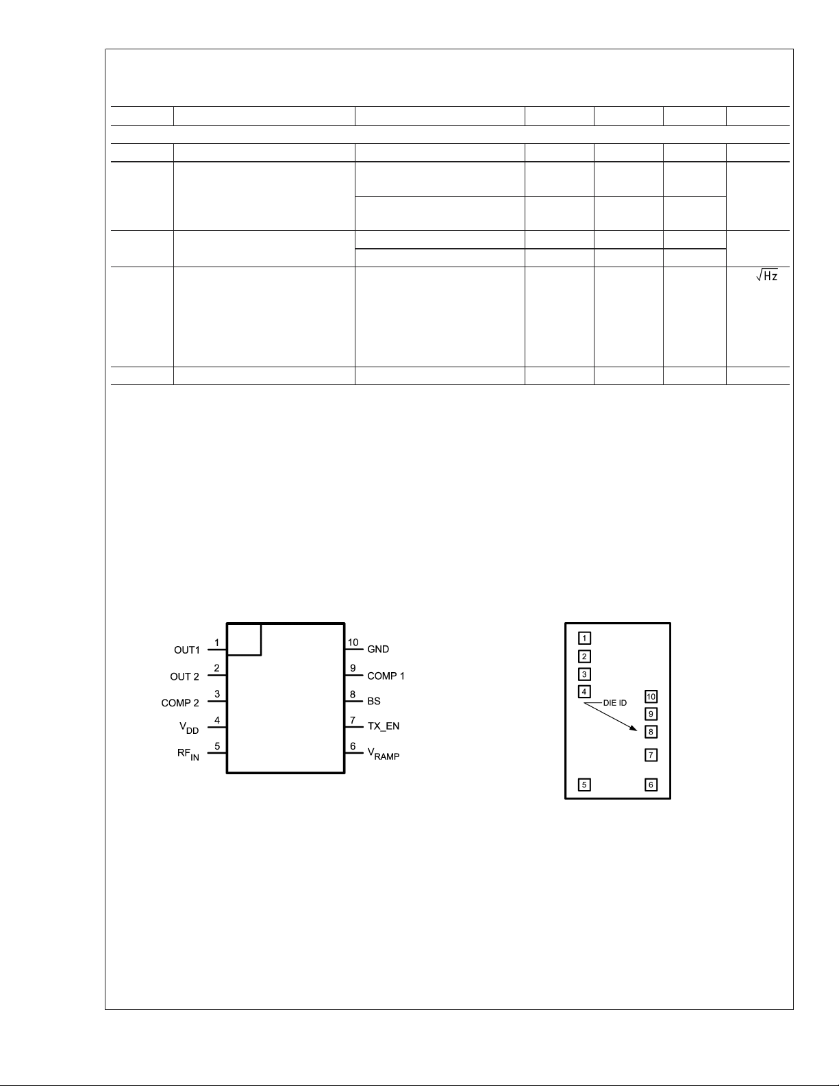
Connection Diagrams
LLP-10 Bond Pad Layout
Top View
20079502
20079503
Top View
www.national.com 4
Bond Pad mechanical Dimensions
X/Y Coordinates Pad Size
Signal Name Pad Number X Y X Y
Out 1 1 −281 617 92 92
Out 2 2 −281 490 92 92
Comp2 3 −281 363 92 92
V
RF
V
DD
IN
RAMP
4 −281 236 92 92
5 −281 −617 92 92
6 281 −617 92 92
TX_EN 7 281 −360 92 92
BS 8 281 −118 92 92
Comp1 9 281 20 92 92
GND 10 281 187 92 92
Note: Dimensions of the bond pad coordinates are in µm Origin of the coordinates: center of the die Coordinates refer to the center of the bond pad
Pin Descriptions
Pin Name Description
Power Supply 4 V
DD
10 GND Power Ground
Digital Inputs 7 TX_EN Schmitt-triggered logic input. A LOW shuts down the whole
8 BS Schmitt-triggered Band Select pin. When BS = H, channel 1
Analog Inputs 5 RF
6V
IN
RAMP
Compensation 9 Comp1 Connects an external RC network between the Comp1 pin
3 Comp2 Frequency compensation pin. The BS signal switches this pin
Output 1 Out1 This pin is connected to the PA of either channel 1 or
2 Out2
Positive Supply Voltage
chip for battery saving purposes. A HIGH enables the chip.
(OUT1) is selected, when BS = L, channel 2 (OUT2) is
selected.
RF Input connected to the Coupler output with optional
attenuation to measure the Power Amplifier (PA) / Antenna
RF power levels.
Sets the RF output power level. The useful input voltage
range is from 0.2V to 1.8V, although voltages from 0V to V
are allowed.
and the Comp2 pin for an overall loop compensation and to
control the closed loop frequency response. Conventional
loop stability techniques can be used in selecting this
network, such as Bode plots. A good starting value for the
RC combination will beC=68pFandR=0Ω.
either to OUT1 or to OUT2.
channel 2.
LMV242
DD
Note: 1. All inputs and outputs are referenced to GND (pin 10).
<
2. For the digital inputs, a LOW is
3. RF power detection is performed internally in the LMV242 and only an RF power coupler with optional extra attenuation has to be used.
0.8V and a HIGH is>1.8V.
www.national.com5

Ordering Information
LMV242
Package Part Number Package Marking Transport Media NSC Drawing
10-Pin LLP
Tested and Wafer
Form
Block Diagram
LMV242LD
LMV242LDX 4.5k Units tape and Reel
LMV242MDA
LMV242MWA 25 Wafer/Vial W008
242LD
No Mark
1k Units Tape and Reel
300 Units Waffle Pack DA0620035
LDA10A
20079504
www.national.com 6

LMV242
Typical Performance Characteristics Unless otherwise specified, V
Supply Current vs. Supply Voltage V
20079505
V
and Log Conformance vs. RF Input Power
OUT
@
900 MHz
and Log Conformance vs. RF Input Power
OUT
V
and Log Conformance vs. RF Input Power
OUT
@
= +2.6V, TJ= 25˚C.
DD
1800 MHz
20079506
V
and Log Conformance vs. RF Input Power
OUT
@
1900 MHz
20079507 20079508
V
and Log Conformance vs. RF Input Power
OUT
20079514 20079515
@
2000 MHz
www.national.com7

Typical Performance Characteristics Unless otherwise specified, V
25˚C. (Continued)
LMV242
Logarithmic Slope vs. Frequency Logarithmic Intercept vs. Frequency
= +2.6V, TJ=
DD
20079516
RF Input Impedance vs. Frequency
@
Resistance and Reactance Gain and Phase vs. Frequency
20079518
I
COMP
vs. V
RAMP
PINvs. V
RAMP
20079517
20079519
20079520 20079521
www.national.com 8

LMV242
Typical Performance Characteristics Unless otherwise specified, V
25˚C. (Continued)
Sourcing Current vs. Output Voltage Sinking Current vs. Output Voltage
20079510 20079511
Output Voltage vs. Sourcing Current Output Voltage vs. Sinking Current
= +2.6V, TJ=
DD
Closed Loop P
OUT
(PA) vs. V
RAMP
20079512
@
GSM 900 MHz Band
20079522 20079523
Closed Loop P
OUT
(PA) vs. V
Band
RAMP
20079513
@
DCS 1800 MHz
www.national.com9

Typical Performance Characteristics Unless otherwise specified, V
25˚C. (Continued)
LMV242
Closed Loop P
Closed Loop DCS-1800 MHz Band Closed Loop PCS-1900 MHz Band
OUT
(PA) vs. V
Band Closed Loop GSM- 900 MHz Band
RAMP
@
PCS 1900 MHz
20079524
= +2.6V, TJ=
DD
20079525
20079526 20079527
www.national.com 10

Application Section
POWER CONTROL PRINCIPLES
The LMV242 is a member of the power loop controller family
of National Semiconductor, for quad-band TDMA/GSM solutions. The typical application diagram demonstrates a basic
approach for implementing the quad-band solution around
an RF Power Amplifier (PA). The LMV242 contains a 50 dB
Logamp detector and interfaces directly with the directional
coupler.
The LMV242 Base Band (control-) interface consists of 3
signals: TX_EN to enable the device, BS to select either
output 1 or output 2 and V
the specified level. The LMV242 gives maximum flexibility to
meet GSM frequency- and time mask criteria for many different single supply Power Amplifier types like HBT or MesFET in GaAs, SiGe or Si technology. This is accomplished by
the programmable Ramp characteristic from the Base Band
and the TX_EN signal along with the external compensation
capacitor.
POWER AMPLIFIER CONTROLLED LOOP
This section gives a general overview and understanding of
how a typical Power Amplifier control loop works and how to
solve the most common problems confronted in the design.
to set the RF output power to
RAMP
voltage (V
transfer function. It is a function of the controller’s V
voltage. Based upon the value of V
) of the PA is of no consequence to the overall
APC
, the PA controller
RAMP
RAMP
will set the gain control voltage of the PA to a level that is
necessary to produce the desired output level. Any temperature dependency in the PA gain control function will be
eliminated. Also, non-linearity’s in the gain transfer function
of the PA do not appear in the overall transfer function (P
vs. V
). The only requirement is that the gain control
RAMP
OUT
function of the PA has to be monotonic. To achieve this, it is
crucial, that the LMV242’s detector is temperature stable.
Typical PA Closed Loop Control Setup
A typical setup of PA control loop is depicted in Figure 1.
Beginning at the output of the Power Amplifier (PA), this
signal is fed, usually via a directional coupler, to a detector.
The error between the detector output current I
ramp current I
, representing the selected power setting,
RAMP
DET
and the
drives the inverting input of an op amp, configured as an
integrator. A reference voltage drives the non-inverting input
of the op amp. Finally the output of the integrator op amp
drives the gain control input of the power amplifier, which
sets the output power. The loop is stabilized when I
equal to I
. Lets examine how this circuit works in detail.
RAMP
DET
LMV242
is
General Overview
The key benefit of a PA control loop circuit is its immunity to
changes in the PA gain control function. When a PA controller is used, the relationship between gain and gain control
FIGURE 1. PA Control Loop
20079528
www.national.com11

Application Section (Continued)
We will assume initially that the output of the PA is at some
LMV242
low level and that the V
converter converts the V
. This current can only come from the integrator ca-
I
RAMP
pacitor C. Current flow from this direction increases the
output voltage of the integrator. The output voltage, which
drives the V
of the PA, increases the gain (we assume
APC
that the PA’s gain control input has a positive sense, that is,
increasing voltage increases gain). The gain will increase,
thereby increasing the amplifier’s output level until the detector output current equals the ramp current I
point, the current through the capacitor will decrease to zero
and the integrator output will be held constant, thereby settling the loop. If capacitor charge is lost over time, output
voltage will decrease. However, this leakage will quickly be
corrected by additional current from the detector. The loop
stabilizes to I
between the V
DET=IRAMP
set voltage and the PA output power,
RAMP
independent of the PA’s V
Power Control Over Wide Dynamic Range
The circuit as described so far, has been designed to produce a temperature independent output power level. If the
detector has a high dynamic range, the circuit can precisely
set PA output levels over a wide power range. To set a PA
output power level, the reference voltage, V
To estimate the response of P
of the LMV242 should be known (P
as discussed is section 3).
The relation between P
IN
of 2 curves:
I
•
•
I
OUT
vs, V
COMP
V
OUT
RAMP
vs. RF Input Power (detection curve)
can be calculated by dividing the V
curve by the feedback resistor used for measuring. With the
knowledge that I
function P
IN
vs. V
COMP=IOUT
is shown in Figure 2. Extra attenua-
RAMP
tion should be inserted between PA output and LMV242’s
to match their dynamic ranges.
P
IN
voltage is at 1V. The V/I
RAMP
voltage to a sinking current
RAMP
thereby creating a direct relation
APC-POUT
and V
characteristics.
vs. V
OUT
RAMP,PIN
OUT=PIN
can be constructed out
RAMP
OUT
RAMP
of the detection
in a closed loop the resulting
. At that
RAMP
, is varied.
vs. V
RAMP
+ attenuation
Using a closed loop to control the PA has benefits over the
use of a directly controlled PA. Non-linearity’s and temperature variations present in the PA transfer function do not
appear in the overall transfer function, P
OUT
vs. V
RAMP
The
response of a typical closed loop is given in Figure 3. The
shape of this curve is determined by the response of the
controller’s detector. Therefore the detector needs to be
accurate, temperature stable and preferably linear in dB to
achieve a accurately controlled output power. The only requirement for the control loop is that the gain control function
of the PA has to be monotonic. With a linear in dB detector,
the relation between V
and PA output power becomes
RAMP
linear in dB as well, which makes calibration of the system
easy.
20079522
FIGURE 3. Closed Loop Response
The response time of the loop can be controlled by varying
the RC time constant of the integrator. Setting this at a low
level will result in fast output settling but can result in ringing
in the output envelope. Setting the RC time constant to a
high value will give the loop good stability but will increase
settling time.
20079521
FIGURE 2. PINvs. V
www.national.com 12
RAMP
ATTENUATION BETWEEN COUPLER AND LMV242
DETECTOR
Figure 4 shows a practical RF power control loop realized by
using the National’s LMV242 with integrated RF detector.
The RF signal from the PA passes through a directional
coupler on its way to the antenna. Directional couplers are
characterized by their coupling factor, which is in the 10 dB
to 30 dB range, typical 20 dB. Because the coupled output
must in its own right deliver some power (in this case to the
detector), the coupling process takes some power from the
main output. This manifests itself as insertion loss, the insertion loss being higher for lower coupling factors.
It is very important to choose the right attenuation between
PA output and detector input to achieve power control over
the full output power range of the PA. A typical value for the
output power of the PA is +35.5 dBm for GSM and +30 dBm
for PCS/DCS. In order to accommodate these levels into the
LMV242 detection range the minimum required total attenuation is about 35 dBm (please refer to typical performance
characteristics in the datasheet and Figure 2). A typical
coupler factor is 20 dB. An extra attenuation of about 15 dB
should be inserted.

Application Section (Continued)
Extra attenuation Z between the coupler and the RF input of
the LMV242 can be achieved by 2 resistors R
according to Figure 3, where
Z = 20 LOG (R
/[RIN+RY])
IN
or
e.g. RY= 300Ω results in an attenuation of 16.9 dB.
To prevent reflection back to the coupler the impedance
seen by the coupler should be 50Ω (R
consists of R
in parallel with RY+RIN.RXcan be calculated
X
). The impedance
O
with the formula:
=[RO*(RY+RIN)]/R
R
X
Y
RX=50*[1+(50/RY)]
e.g. with R
= 300Ω,RIN=50Ω→RX=58Ω.
Y
X
and R
LMV242
about 206 mV, so offset voltages in the DAC or amplifier
supplying the R
output and increased power consumption.
Y
Transmit Enable
Power consumption requirements are supported by the
TX_EN function, which puts the entire chip into a power
saving mode to enable maximum standby and talk time while
ensuring the output does not glitch excessively during
Power-up and Power-down. The device will be active in the
case TX_EN = High, or otherwise go to a low power consumption shutdown mode. During shutdown the output is
pulled low to minimize the output voltage.
Band Select
The LMV242 is especially suitable for PA control loops with 2
PA’s. The 2 outputs to steer the V
controlled with the band select pin. When the band select is
LOW output2 is selected, while output1 is selected when
band select is HIGH. The not-selected output is pulled low.
Analog Output
The output is driven by a rail-to-rail amplifier capable of both
sourcing and sinking. Several curves are given in the “Typical performance characteristics”-section regarding the output. The output voltage vs. sourcing/sinking current curves
show the typical voltage drop from the rail over temperature.
The sourcing/sinking current vs. output voltage characteristics show the typical charging/discharging current, which the
output is capable of delivering at a certain voltage. The
output is free from glitches when enabled by TX_EN. When
TX_EN is low, the selected output voltage is fixed or near
GND.
signal will not cause excess RF signal
AMP
of the PA’s can be
APCS
20079530
FIGURE 4. Simplified PA Control Loop with Extra
Attenuation
BASEBAND CONTROL OF THE LMV242
The LMV242 has 3 baseband-controlled inputs:
V
•
•
signal (Base band DAC ramp signal)
RAMP
TX_EN is a digital signal (performs the function
“Shutdown/Transmit Enable”).
Band Select (BS)
•
V
Signal
RAMP
The actual V
input value sets the RF output power. By
RAMP
applying a certain mask shape to the “Ramp in” pin, the
output voltage level of the LMV242 is adjusting the PA
control voltage to get a power level (P
/dBm) out of the
OUT
PA, which is proportional to the single ramp voltage steps.
The recommended V
trol is 0.2V to 2.0V. The V
from 0V to V
without malfunction or damage. The V
DD
voltage range for RF power con-
RAMP
input will tolerate voltages
RAMP
RAMP
input does not change the output level until the level reaches
FREQUENCY COMPENSATION
To compensate and prevent the closed loop arrangement
from oscillations and overshoots at the output of the RF
detector/error amplifier of the LMV242, the system can be
adjusted by means of external RC components connected
between Comp1 and Comp2. Exact values heavily depend
on PA characteristics. A good starting point isR=0Ω and
C = 68 pF. The vast combination of PA’s and couplers
available preclude a generalized formula for choosing these
components. Additional frequency compensation of the
closed loop system can be achieved by adding a resistor
(and if needed an inductor) between the LMV242’s output
and the V
input of the PA. Please contact National Semi-
APC
conductor for additional support.
TIMING DIAGRAM
In order to meet the timemask specifications for GSM, a
good timing between the control signals and the RF signal is
essential. According to the specifications the PA’s RF output
power needs to ramp within 28 µsec with minimum overshoot. To achieve this, the output of the PA controller should
ramp at the same time as the RF signal from the Base Band.
The ramp signal sets the controllers output to the required
value, where the loop needs a certain time to set this output.
Therefore the ramp should be set high some time before the
output has to be high. How much time depends on the setup
and the PA used. If the controllers shutdown functionality is
used, the shutdown should be set high about 6 µsec before
the ramp is set high.
www.national.com13

Application Section (Continued)
The control loop can be configured by the following vari-
LMV242
ables:
Lead time TX_EN event vs. start GSM burst
•
Lead time V
•
Ramp profile
•
Loop compensation
•
vs. start GSM burst
RAMP
20079531
FIGURE 5. Timing V
vs. RF Signal
RAMP
www.national.com 14

10-Pad Bare Die
LMV242
20079503
Die / Wafer Characteristics
Fabrication Attributes
Physical Die Identification LMV242A
Die Step A
Physical Attributes
Wafer Diameter 200 mm
Die Size (Drawn) 889 µm x 1562 µm
35.0 mils x 61.5 mils
Thickness 216 µm Nominal
Min Pitch 123 µm Nominal
General Die Information
Bond Pad Opening Size (min) 92 µm x 92µm
Bond Pad Metallization 0.5% Copper_Bal.
Aluminum
Passivation VOM Nitride
Back Side Metal Bare Back
Back Side Connection Floating
Note: Note: Actual die size is rounded to the nearest micron
www.national.com15

Physical Dimensions inches (millimeters)
unless otherwise noted
10-Pin LLP
NS Package Number LDA10A
LMV242 Dual Output, Quad-Band GSM/GPRS Power Controller
LIFE SUPPORT POLICY
NATIONAL’S PRODUCTS ARE NOT AUTHORIZED FOR USE AS CRITICAL COMPONENTS IN LIFE SUPPORT
DEVICES OR SYSTEMS WITHOUT THE EXPRESS WRITTEN APPROVAL OF THE PRESIDENT AND GENERAL
COUNSEL OF NATIONAL SEMICONDUCTOR CORPORATION. As used herein:
1. Life support devices or systems are devices or
systems which, (a) are intended for surgical implant
into the body, or (b) support or sustain life, and
whose failure to perform when properly used in
accordance with instructions for use provided in the
labeling, can be reasonably expected to result in a
significant injury to the user.
BANNED SUBSTANCE COMPLIANCE
National Semiconductor certifies that the products and packing materials meet the provisions of the Customer Products
Stewardship Specification (CSP-9-111C2) and the Banned Substances and Materials of Interest Specification
(CSP-9-111S2) and contain no ‘‘Banned Substances’’ as defined in CSP-9-111S2.
2. A critical component is any component of a life
support device or system whose failure to perform
can be reasonably expected to cause the failure of
the life support device or system, or to affect its
safety or effectiveness.
National Semiconductor
Americas Customer
Support Center
Email: new.feedback@nsc.com
Tel: 1-800-272-9959
www.national.com
National does not assume any responsibility for use of any circuitry described, no circuit patent licenses are implied and National reserves the right at any time without notice to change said circuitry and specifications.
National Semiconductor
Europe Customer Support Center
Fax: +49 (0) 180-530 85 86
Email: europe.support@nsc.com
Deutsch Tel: +49 (0) 69 9508 6208
English Tel: +44 (0) 870 24 0 2171
Français Tel: +33 (0) 1 41 91 8790
National Semiconductor
Asia Pacific Customer
Support Center
Email: ap.support@nsc.com
National Semiconductor
Japan Customer Support Center
Fax: 81-3-5639-7507
Email: jpn.feedback@nsc.com
Tel: 81-3-5639-7560
 Loading...