

August 2004
LMV225/LMV226/LMV228
RF Power Detector for CDMA and WCDMA in micro SMD
LMV225/LMV226/LMV228 RF Power Detector for CDMA and WCDMA in micro SMD
General Description
The LMV225/LMV226/LMV228 are 30dB RF power detectors intended for use in CDMA and WCDMA applications.
The device has an RF frequency range from 450 MHz to 2
GHz. It provides an accurate temperature and supply compensated output voltage that relates linearly to the RF input
power in dBm. The circuit operates with a single supply from
2.7V to 5.5V. The LMV225/LMV226/LMV228 have an integrated filter for low-ripple average power detection of CDMA
signals with 30 dB dynamic range. Additional filtering can be
applied using a single external capacitor.
The LMV225 has an RF power detection range from –30
dBm to 0 dBm and is ideally suited for direct use in combination with resistive taps. The LMV226/LMV228 have a detection range from –15 dBm to 15 dBm and are intended for
use in combination with a directional coupler. The LMV226 is
equipped with a buffered output which makes it suitable for
GSM, EDGE, GPRS and TDMA applications.
The device is active for Enable = HI, otherwise it is in a low
power consumption shutdown mode. During shutdown the
output will be LOW. The output voltage ranges from 0.2V to
2V and can be scaled down to meet ADC input range requirements.
The LMV225/LMV226/LMV228 power detectors are offered
in the small 1.0 mm x 1.0 mm X 0.6 mm micro SMD package.
Features
n 30 dB linear in dB power detection range
n Output voltage range 0.2 to 2V
n Logic low shutdown
n Multi-band operation from 450 MHz to 2000 MHz
n Accurate temperature compensation
n micro SMD package 1.0 mm x 1.0 mm x 0.6 mm
Applications
n CDMA RF power control
n WCDMA RF power control
n CDMA2000 RF power control
n PA modules
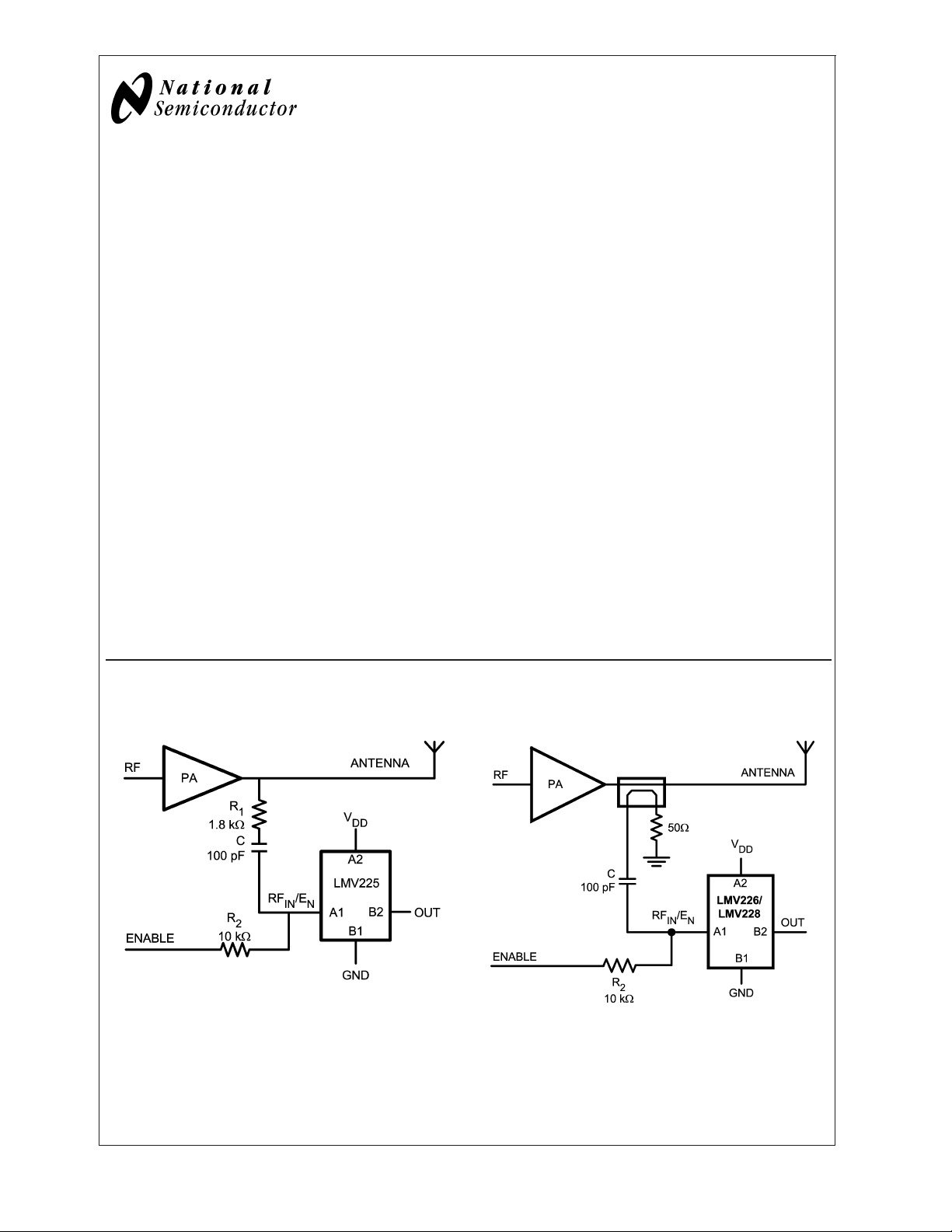
Typical Application
LMV225
LMV226/LMV228
20076001
20076046
© 2004 National Semiconductor Corporation DS200760 www.national.com
Absolute Maximum Ratings (Note 1)
If Military/Aerospace specified devices are required,
please contact the National Semiconductor Sales Office/
Distributors for availability and specifications.
Supply Voltage
- GND 6.0V Max
V
DD
ESD Tolerance (Note 2)
Human Body Model 2000V
LMV225/LMV226/LMV228
Machine Model 200V
Junction Temperature (Note 3) 150˚C Max
Mounting Temperature
Infrared or convection (20 sec) 235˚C
Operating Ratings (Note 1)
Supply Voltage 2.7V to 5.5V
Temperature Range −40˚C to +85˚C
RF Frequency Range 450 MHz to 2 GHz
Storage Temperature Range −65˚C to 150˚C
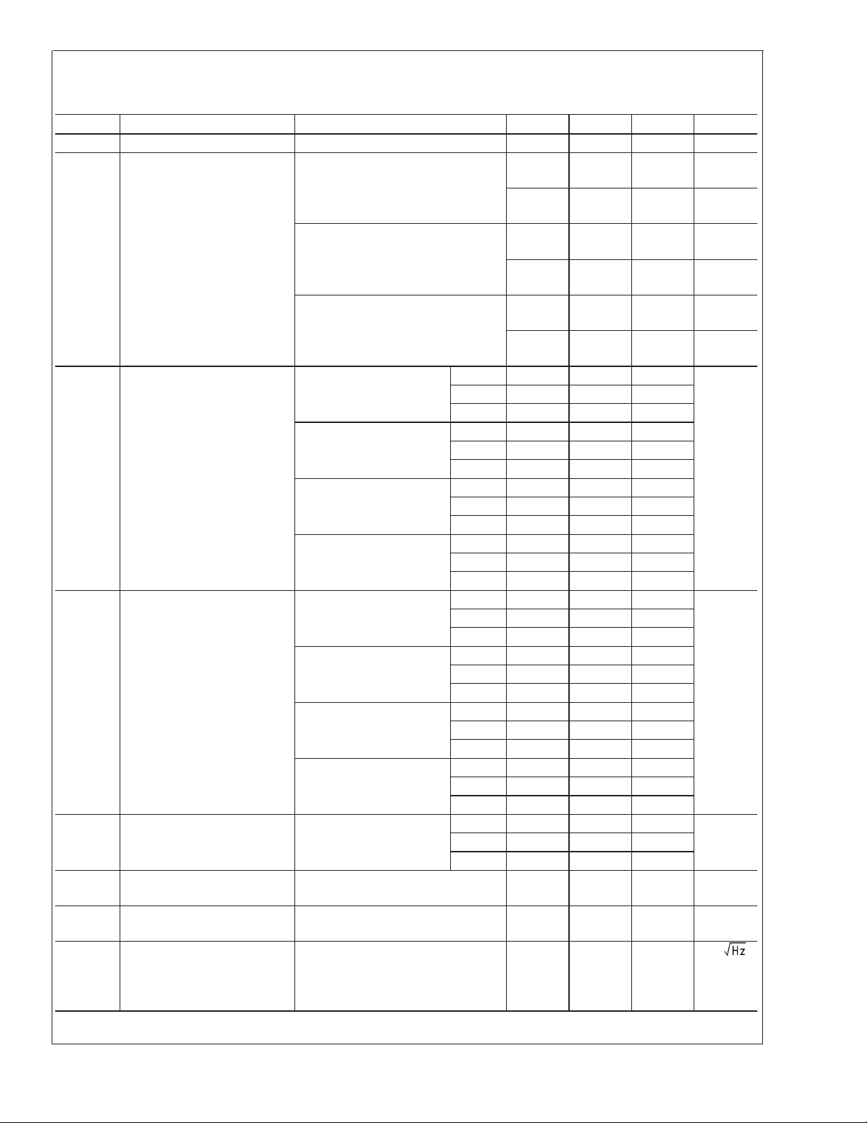
2.7 DC and AC Electrical Characteristics
Unless otherwise specified, all limits are guaranteed to VDD= 2.7V; TJ= 25˚C. Boldface limits apply at temperature extremes.
(Note 4)
Symbol Parameter Condition Min Typ Max Units
I
DD
V
LOW
V
HIGH
t
on
t
r
I
EN
P
IN
Supply Current Active Mode: RFIN/EN=
(DC), No RF Input
V
DD
Power Present
LMV225 4.8 7
8
LMV226 4.9 6.2
8
LMV228 4.9 6.2
8
Shutdown: RF
= GND (DC), No
IN/EN
0.44 4.5 µA
RF Input Power Present
ENLogic Low Input Level
0.8 V
(Note 6)
ENLogic High Input Level
1.8 V
(Note 6)
Turn-on-Time (Note 9) No RF Input Power
LMV225 2.1
Present, Output Loaded
with 10pF
Rise Time (Note 7) Step from no Power to 0
LMV228 1.7
LMV225 4.5
dBm Applied, Output
Loaded with 10pF
Step from no Power to 15
dBm Applied, Output
Loaded with 10pF
LMV226 1.8
LMV228 4.8
Current into RFIN/ENPin 1 µA
Input Power Range (Note 5) LMV225 −30
0
−43
−13
LMV226 −15
15
−28
2
LMV228 −15
15
−28
2
mA
µsLMV226 1.2
µs
dBm
dBV
dBm
dBV
dBm
dBV
www.national.com 2
2.7 DC and AC Electrical Characteristics (Continued)
Unless otherwise specified, all limits are guaranteed to VDD= 2.7V; TJ= 25˚C. Boldface limits apply at temperature extremes.
(Note 4)
Symbol Parameter Condition Min Typ Max Units
Logarithmic Slope (Note 8) 900 MHz LMV225 44.0
LMV226 44.5
LMV228 44.0
1800 MHz LMV225 39.4
LMV226 41.6
V
I
R
e
OUT
n
OUT
OUT
LMV228 41.9
1900 MHz LMV225 38.5
LMV226 41.2
LMV228 41.6
2000 MHz LMV225 38.5
LMV226 41.0
LMV228 41.2
Logarithmic Intercept (Note 8) 900 MHz LMV225 −45.5
LMV226 −24.5
LMV228 −27.2
1800 MHz LMV225 −46.6
LMV226 −25.1
LMV228 −28.2
1900 MHz LMV225 −46.3
LMV226 −24.9
LMV228 −28.0
2000 MHz LMV225 −46.7
LMV226 −24.7
LMV228 −28.0
Output Voltage No RF Input Power
LMV225 214 350
Present
LMV228 228 350
Output Current
LMV226 Only 4.5 5.3 mA
Sourcing/Sinking
Output Impedance LMV225/LMV228 only, no RF Input
19.8 29
Power Present
Output Referred Noise RF Input = 1800 MHz, −10 dBm for
700
LMV225 and 5 dBm for
LMV226/LMV228, Measured at
10 kHz
34
mV/dB
dBm
mVLMV226 223 350
nV/
LMV225/LMV226/LMV228
kΩ
www.national.com3
2.7 DC and AC Electrical Characteristics (Continued)
Unless otherwise specified, all limits are guaranteed to VDD= 2.7V; TJ= 25˚C. Boldface limits apply at temperature extremes.
(Note 4)
Symbol Parameter Condition Min Typ Max Units
Variation Due to Temperature 900 MHz, RF
LMV225/LMV226/LMV228
= 0 dBm
IN
Referred to 25˚C
900 MHz, RF
= 15 dBm
IN
Referred to 25˚C
1800 MHz, RF
= 0 dBm
IN
Referred to 25˚C
1800 MHz, RFIN= 15 dBm
Referred to 25˚C
1900 MHz, RF
= 0 dBm
IN
Referred to 25˚C
1900 MHz, RF
= 15 dBm
IN
Referred to 25˚C
2000 MHz, RF
= 0 dBm
IN
Referred to 25˚C
2000 MHz, RF
= 15 dBm
IN
Referred to 25˚C
LMV225 +0.64
−1.07
LMV226 +0.05
−0.02
LMV228 +0.22
−0.36
LMV225 +0.09
−0.86
LMV226 +0.07
−0.10
LMV228 +0.29
−0.57
LMV225 +0
−0.69
LMV226 +0
−0.10
LMV228 +0.23
−0.64
LMV225 +0
−0.86
LMV226 +0
−0.29
LMV228 +0.27
−0.65
dB
5.0 DC and AC Electrical Characteristics
Unless otherwise specified, all limits are guaranteed to VDD= 5.0V; TJ= 25˚C. Boldface limits apply at temperature extremes.
(Note 4)
Symbol Parameter Condition Min Typ Max Units
I
DD
V
LOW
V
HIGH
t
on
t
r
Supply Current Active Mode: RFIN/EN=
(DC), no RF Input
V
DD
Power Present.
Shutdown: RF
= GND (DC), no
IN/EN
RF Input Power Present.
ENLogic Low Input Level
(Note 6)
ENLogic High Input Level
(Note 6)
Turn-on-Time (Note 9) No RF Input Power
Present, Output Loaded
with 10pF
Rise Time (Note 7) Step from no Power to 0
dBm Applied, Output
Loaded with 10pF
Step from no Power to 15
dBm Applied, Output
Loaded with 10pF
LMV225 5.3 7.5
9
LMV226 5.3 6.8
9
LMV228 5.4 6.8
9
0.32 4.5 µA
0.8 V
1.8 V
LMV225 2.1
LMV228 1.7
LMV225 4.5
LMV226 1.4
LMV228 4.8
mA
µsLMV226 1.0
µs
www.national.com 4
5.0 DC and AC Electrical Characteristics (Continued)
Unless otherwise specified, all limits are guaranteed to VDD= 5.0V; TJ= 25˚C. Boldface limits apply at temperature extremes.
(Note 4)
Symbol Parameter Condition Min Typ Max Units
I
P
V
I
R
e
EN
IN
OUT
OUT
OUT
n
Current Into RFIN/ENPin 1 µA
Input Power Range (Note 5) LMV225 −30
dBm
0
−43
dBV
−13
LMV226 −15
dBm
15
−28
dBV
2
LMV228 −15
dBm
15
−28
dBV
2
Logarithmic Slope (Note 8) 900 MHz LMV225 44.6
LMV226 44.6
LMV228 44.2
1800 MHz LMV225 40.6
LMV226 42.2
LMV228 42.4
1900 MHz LMV225 39.6
mV/dB
LMV226 41.8
LMV228 42.2
2000 MHz LMV225 39.7
LMV226 41.6
LMV228 41.8
Logarithmic Intercept (Note 8) 900 MHz LMV225 −47.0
LMV226 −25.0
LMV228 −27.7
1800 MHz LMV225 −48.5
LMV226 −25.7
LMV228 −28.9
1900 MHz LMV225 −48.2
dBm
LMV226 −25.6
LMV228 −28.7
2000 MHz LMV225 −48.9
LMV226 −25.5
LMV228 −28.7
Output Voltage No RF Input Power
Present
LMV225 222 400
mVLMV226 231 400
LMV228 244 400
Output Current
LMV226 Only 4.5 5.3 mA
Sourcing/Sinking
Output Impedance No RF Input Power Present 23.7 29
31
Output Referred Noise RF Input = 1800 MHz, −10 dBm for
700 nV/
LMV225 and 5 dBm for
LMV226/LMV228, Measured at
10 kHz
LMV225/LMV226/LMV228
kΩ
www.national.com5

5.0 DC and AC Electrical Characteristics (Continued)
Unless otherwise specified, all limits are guaranteed to VDD= 5.0V; TJ= 25˚C. Boldface limits apply at temperature extremes.
(Note 4)
Symbol Parameter Condition Min Typ Max Units
Variation Due to Temperature 900 MHz, RF
= 0 dBm
IN
Referred to 25˚C
900 MHz, RF
= 15 dBm
IN
Referred to 25˚C
LMV225/LMV226/LMV228
1800 MHz, RF
Referred to 25˚C
1800 MHz, RFIN= 15 dBm
Referred to 25˚C
1900 MHz, RF
Referred to 25˚C
1900 MHz, RF
Referred to 25˚C
2000 MHz RF
Referred to 25˚C
2000 MHz RF
Referred to 25˚C
Note 1: Absolute Maximum Ratings indicate limits beyond which damage to the device may occur. Operating Ratings indicate conditions for which the device is
intended to be functional, but specific performance is not guaranteed. For guaranteed specifications and the test conditions, see the Electrical Characteristics.
Note 2: Human body model: 1.5 kΩ in series with 100 pF. Machine model, 0Ω in series with 100 pF.
Note 3: The maximum power dissipation is a function of T
(T
J(MAX)-TA
Note 4: Electrical Table values apply only for factory testing conditions at the temperature indicated. Factory testing conditions result in very limited self-heating of
the device such that T
Note 5: Power in dBV = dBm + 13 when the impedance is 50Ω.
Note 6: All limits are guaranteed by design or statistical analysis
Note 7: Typical values represent the most likely parametric norm.
Note 8: Device is set in active mode with a 10 kΩ resistor from V
pin using a 100 pF coupling capacitor.
Note 9: Turn-on time is measured by connecting a 10 kΩ resistor to the RF
of resistor R
)/θJA. All numbers apply for packages soldered directly into a PC board
. No guarantee of parametric performance is indicated in the electrical tables under conditions of internal self-heating where T
J=TA
and capacitor C adds an additional delay.
2
, θJAand TA. The maximum allowable power dissipation at any ambient temperature is PD=
J(MAX)
DD
= 0 dBm
IN
= 0 dBm
IN
= 15 dBm
IN
= 0 dBm
IN
= 15 dBm
IN
to RFIN/EN. RF signal is applied using a 50Ω RF signal generator AC coupled to the RFIN/E
pin. Be aware that in the actual application on the front page, the RC-time constant
IN/EN
LMV225 +0.89
−1.16
LMV226 +0.25
−0.16
LMV228 +0.46
−0.62
LMV225 +0.3
−0.82
LMV226 +0.21
−0.09
LMV228 +0.55
−0.78
LMV225 +0.34
−0.63
LMV226 +0.21
−0.19
LMV228 +0.55
−0.93
LMV225 +0.22
−0.75
LMV226 +0.25
−0.34
LMV228 +0.61
−0.91
dB
>
TA.
J
N
www.national.com 6

Connection Diagram
LMV225/LMV226/LMV228
4-Bump micro SMD
Top View
20076002
Pin Description
Pin Name Description
Power Supply A2 V
B1 GND Power Ground
A1 RF
Output B2 Out Ground referenced detector output voltage (linear in dBm)
DD
IN/EN
Positive Supply Voltage
DC voltage determines enable state of the device (HIGH = device active). AC voltage is
the RF input signal to the detector (beyond 450 MHz). The RF
terminated with 50Ω in series with 45 pF.
pin is internally
IN/EN
Ordering Information
Package Part Number Package Marking Transport Media NSC Drawing
LMV225TL
LMV225TLX 3k Units Tape and Reel
4-Bump micro SMD
Note: This product is only offered with lead free bumps.
LMV226TL
LMV226TLX 3k Units Tape and Reel
LMV228TL
LMV228TLX 3k Units Tape and Reel
I
I
I
250 Units Tape and Reel
250 Units Tape and Reel
250 Units Tape and Reel
TLA04AAA
www.national.com7

Block Diagrams
LMV225/LMV226/LMV228
LMV225
LMV226
20076003
20076049
LMV228
www.national.com 8
20076047

LMV225/LMV226/LMV228
Typical Performance Characteristics Unless otherwise specified, V
= 2.7V, TJ= 25˚C.
DD
Supply Current vs. Supply Voltage (LMV225) Supply Current vs. Supply Voltage (LMV226)
20076004 20076051
Supply Current vs. Supply Voltage (LMV228) Output Voltage vs. RF Input Power (LMV225)
20076034
20076005
Output Voltage vs. RF Input Power (LMV226) Output Voltage vs. RF Input Power (LMV228)
20076052 20076035
www.national.com9

Typical Performance Characteristics Unless otherwise specified, V
25˚C. (Continued)
= 2.7V, TJ=
DD
Output Voltage and Log Conformance vs.
RF Input Power
LMV225/LMV226/LMV228
Output Voltage and Log Conformance vs.
RF Input Power
@
900 MHz (LMV225)
@
900 MHz (LMV228)
20076006
Output Voltage and Log Conformance vs.
RF Input Power@900 MHz (LMV226)
20076053
Output Voltage and Log Conformance vs.
RF Input Power@1800 MHz (LMV225)
20076036
Output Voltage and Log Conformance vs.
@
RF Input Power
www.national.com 10
1800 MHz (LMV226)
20076054 20076037
20076007
Output Voltage and Log Conformance vs.
RF Input Power@1800 MHz (LMV228)

LMV225/LMV226/LMV228
Typical Performance Characteristics Unless otherwise specified, V
25˚C. (Continued)
Output Voltage and Log Conformance vs.
RF Input Power
@
1900 MHz (LMV225)
Output Voltage and Log Conformance vs.
@
RF Input Power
1900 MHz (LMV228)
20076008
Output Voltage and Log Conformance vs.
RF Input Power@1900 MHz (LMV226)
Output Voltage and Log Conformance vs.
RF Input Power@2000 MHz (LMV225)
= 2.7V, TJ=
DD
20076055
Output Voltage and Log Conformance vs.
@
RF Input Power
2000 MHz (LMV226)
20076038
20076009
Output Voltage and Log Conformance vs.
RF Input Power@2000 MHz (LMV228)
20076056 20076039
www.national.com11

Typical Performance Characteristics Unless otherwise specified, V
25˚C. (Continued)
Logarithmic Slope vs. Frequency (LMV225) Logarithmic Slope vs. Frequency (LMV226)
LMV225/LMV226/LMV228
= 2.7V, TJ=
DD
20076010
20076057
Logarithmic Slope vs. Frequency (LMV228) Logarithmic Intercept vs. Frequency (LMV225)
20076040
20076011
Logarithmic Intercept vs. Frequency (LMV226) Logarithmic Intercept vs. Frequency (LMV228)
20076058 20076041
www.national.com 12

LMV225/LMV226/LMV228
Typical Performance Characteristics Unless otherwise specified, V
25˚C. (Continued)
Output Variation vs. RF Input Power Normalized to 25˚C
@
900 MHz (LMV225)
20076012 20076059
Output Variation vs. RF Input Power Normalized to 25˚C
@
900 MHz (LMV228)
Output Variation vs. RF Input Power Normalized to 25˚C
@
900 MHz (LMV226)
Output Variation vs. RF Input Power Normalized to 25˚C
@
1800 MHz (LMV225)
= 2.7V, TJ=
DD
20076042 20076013
Output Variation vs. RF Input Power Normalized to 25˚C
@
1800 MHz (LMV226)
20076060 20076043
Output Variation vs. RF Input Power Normalized to 25˚C
@
1800 MHz (LMV228)
www.national.com13

Typical Performance Characteristics Unless otherwise specified, V
25˚C. (Continued)
= 2.7V, TJ=
DD
Output Variation vs. RF Input Power Normalized to 25˚C
@
1900 MHz (LMV225)
LMV225/LMV226/LMV228
Output Variation vs. RF Input Power Normalized to 25˚C
@
1900 MHz (LMV228)
20076014
Output Variation vs. RF Input Power Normalized to 25˚C
@
1900 MHz (LMV226)
20076061
Output Variation vs. RF Input Power Normalized to 25˚C
@
2000 MHz (LMV225)
20076044
Output Variation vs. RF Input Power Normalized to 25˚C
@
2000 MHz (LMV226)
20076062
www.national.com 14
20076015
Output Variation vs. RF Input Power Normalized to 25˚C
@
2000 MHz (LMV228)
20076045

LMV225/LMV226/LMV228
Typical Performance Characteristics Unless otherwise specified, V
25˚C. (Continued)
RF Input Impedance vs. Frequency
PSRR vs. Frequency (LMV225, LMV226 and LMV228)
20076023
Reactance (LMV225, LMV226 and LMV228)
= 2.7V, TJ=
DD
@
Resistance and
20076024
www.national.com15

Application Notes
CONFIGURING A TYPICAL APPLICATION
The LMV225/LMV226/LMV228 are power detectors intended for CDMA and WCDMA applications. Power applied
at its input translates to a DC voltage on the output through
a linear-in-dB response. The LMV225 detector is especially
suited for power measurements via a high-resistive tap,
while the LMV226/LMV228 are designed to be used in combination with a directional coupler. The LMV226 has an
LMV225/LMV226/LMV228
additional output voltage buffer and therefore a low output
impedance. The key features of the devices are shown in
table 1.
TABLE 1. DEVICE CHARACTERISTICS
Input Range
(dBm)
LMV225 −30 / 0 No High Resistive Tap
LMV226 −15 / 15 Yes Directional Coupler
LMV228 −15 / 15 No Directional Coupler
In order to match the output power range of the power
amplifier (PA) with the range of the LMV225’s input, the high
resistive tap needs to be configured correctly. In case of the
LMV226/LMV228 the coupling factor of the directional coupler needs to be chosen correctly.
Output
Buffer
Application
Solving this expression for R
, using that RIN=50Ω, yields:
1
(2)
In Figure 1,R
is set to 1800Ω resulting in an attenuation of
1
31.4 dB
DIRECTIONAL COUPLER APPLICATION
The LMV226/LMV228 also has a 50Ω input resistance. However, its input range differs compared to the LMV225, i.e.
−15 dBm to +15 dBm. If a typical attenuation of a directional
coupler is 20 dB, the LMV226/LMV228 can be directly connected via the directional coupler to the PA without the need
of additional external attenuator (Figure 2). Different PA
ranges can be configured using couplers with other coupling
factors.
HIGH RESISTIVE TAP APPLICATION
The constant input impedance of the device enables the
realization of a frequency independent input attenuation to
adjust the LMV225’s range to the range of the PA. Resistor
and the 50Ω input resistance (RIN) of the device realize
R
1
this attenuation (Figure 1). To minimize insertion loss, resis-
needs to be sufficiently large. The following example
tor R
1
demonstrates how to determine the proper value for R
20076033
.
1
FIGURE 1. Typical LMV225 Application with High
Resistive Tap
Suppose the useful output power of the PA ranges up to +31
dBm. As the LMV225 can handle input power levels up to 0
dBm. R
dB. The attenuation realized by R
resistance R
should realize a minimum attenuation of 31-0=31
1
of the detector equals:
IN
and the effective input
1
(1)
20076046
FIGURE 2. Typical LMV226/LMV228 Application with
Directional Coupler
SHUTDOWN FUNCTIONALITY
The LMV225/LMV226/LMV228 RF
pins have 2 func-
IN/EN
tions combined:
Enable/Shutdown
•
Power input
•
The capacitor C and the resistor R
(Figure 1 and Figure 2)
2
separate the DC shutdown functionality from the AC power
measurement. The device is active when Enable = HI, otherwise it is in a low power consumption shutdown mode.
During shutdown the output will be LOW.
Capacitor C should be chosen sufficiently large to ensure a
corner frequency far below the lowest input frequency to be
measured. In case of the LMV225 the corner frequency can
be calculated using:
(3)
Where R
With R
=50Ω,CIN= 45 pF typical.
IN
= 1800Ω and C = 100 pF, this results in a corner
1
frequency of 2.8 MHz. This corner frequency is an indicative
www.national.com 16

Application Notes (Continued)
number. The goal is to have a magnitude transfer, which is
sufficiently flat in the used frequency range; capacitor C
should be chosen significantly larger than capacitor C
assure a proper performance of the high resistive tap. Capacitor C shouldn’t be chosen excessively large since the
RC-time, it introduces in combination with resistor R
to the turn-on time of the device.
The LMV226/LMV228 do not use a resistor R
LMV225. Though a resistor is seen on the coupler side
(R
COUPLER
). Therefore a similar equation holds for the
LMV226/LMV228 LF corner frequency, where R
with the coupler output impedance (R
With R
COUPLER
=50Ω and C = 100 pF, the resulting corner
COUPLER
).
frequency is 50 MHz.
The output voltage is proportional to the logarithm of the
input power, often called “linear-in-dB”. Figure 3 shows the
typical output voltage versus PA output power of the LMV225
setup as depicted in Figure 1.
, adds
2
like the
1
is replaced
1
IN
LMV225/LMV226/LMV228
to
20076017
FIGURE 4. AM Modulated RF Signal
The ripple observed at the output of the detector equals the
detectors response to the power variation at the input due to
AM modulation (Figure 4). This signal has a maximum amplitude V
where 1+µ can be maximum 2 and 1-µ can be minimum 0.
The amplitude of the ripple can be described with the formula:
(1+µ) and a minimum amplitude V
•
IN
(1-µ),
•
IN
20076016
FIGURE 3. Typical power detector response, V
OUT
vs.
PA output Power
OUTPUT RIPPLE DUE TO AM MODULATION
A CDMA modulated carrier wave generally contains some
amplitude modulation that might disturb the RF power measurement used for controlling the PA. This section explains
the relation between amplitude modulation in the RF signal
and the ripple on the output of the LMV225/LMV228. Expressions are provided to estimate this ripple on the output. The
ripple can be further reduced by lowpass filtering at the
output. This is realized by connecting an capacitor from the
output of the LMV225/LMV228 to ground.
Estimating Output Ripple
The CDMA modulated RF input signal of Figure 3 can be
described as:
(t)=VIN[1 + µ(t)] cos (2 · π ·f·t) (4)
V
IN
In which V
is the amplitude of the carrier frequency and the
IN
amplitude modulation µ(t) can be between -1 and 1.
(5)
where V
is the slope of the detection curve (Figure 5) and µ
Y
is the modulation index. Equation (5) can be reduced to:
(6)
Consequently, the ripple is independent of the average input
power of the RF input signal and only depends on the
logarithmic slope V
and the ratio of the maximum and the
Y
minimum input signal amplitude.
For CDMA, the ratio of the maximum and the minimum input
signal amplitude modulation is typically in the order of 5 to 6
dB, which is equivalent to a modulation index µ of 0.28 to
0.33.
A further understanding of the equation above can be
achieved via the knowledge that the output voltage V
OUT
of
the LMV225/LMV228 is linear in dB, or proportional to the
input power P
in dBm. As discussed earlier, CDMA has a
IN
modulation in the order of 5 to 6 dB. Since the transfer is
linear in dB, the output voltage V
will vary linearly over
OUT
about 5 to 6 dB in the curve (Figure 5).
www.national.com17

Application Notes (Continued)
LMV225/LMV226/LMV228
a 1.5 nF capacitor is then 20
log (200/12) = 24.4 dB. This
•
is very close to the calculated number of the previous paragraph.
20076018
FIGURE 5. V
The output voltage variation ∆V
vs. RF Input Power P
OUT
is thus identical for RF
OUT
IN
input signals that fall within the linear range (in dB) of the
detector. In other words, the output variation is independent
of the absolute RF input signal:
In which V
∆V
O=VY
is the slope of the curve. The log-conformance
Y
· ∆P
IN
(7)
error is usually much smaller than the ripple due to AM
modulation. In case of the LMV225/LMV228, V
dB. With ∆P
valid for all V
= 5 dB for CDMA, ∆V
IN
.
OUT
= 200 mVPP. This is
OUT
=40mV/
Y
Output Ripple with Additional Filtering
The calculated result above is for an unfiltered configuration.
When a low pass filter is used by shunting a capacitor of e.g.
= 1.5 nF at the output of the LMV225/LMV228 to
C
OUT
ground, this ripple is further attenuated. The cut-off frequency follows from:
(8)
With the output resistance of the LMV225/LMV228 R
19.8 kΩ typical and C
equals f
= 5.36 kHz. A 100 kHz AM signal then gets attenu-
C
= 1.5 nF, the cut-off frequency
OUT
O
ated by 5.36/100 or 25.4 dB. The remaining ripple will be
less than 20 mV. With a slope of 40 mV/dB this translates
±
into an error of less than
0.5 dB. Since the LMV226 has a
low output impedance buffer, a capacitor to reduce the ripple
will not be effective.
20076025
FIGURE 6. Output Ripple vs. RF Input Power
PRINCIPLE OF OPERATION
The logarithmic response of the LMV225/LMV226/LMV228
is implemented by a logarithmic amplifier as shown in Figure
7. The logarithmic amplifier consists of a number of cascaded linear gain cells. With these gain cells, a piecewise
approximation of the logarithmic function is constructed.
20076019
=
FIGURE 7. Logarithmic Amplifier
Every gain cell has a response according to Figure 8.Ata
certain threshold (E
), the gain cell starts to saturate, which
K
means that the gain drops to zero. The output of gain cell 1
is connected to the input of gain cell 2 and so on.
Output Ripple Measurement
Figure 6 shows the ripple reduction that can be achieved by
adding additional capacitance at the output of the LMV225/
LMV228. The RF signal of 900 MHz is AM modulated with a
100 kHz sinewave and a modulation index of 0.3. The RF
input power is swept while the modulation index remains
unchanged. Without the output capacitor the ripple is about
200 mV
ground, results in a ripple of 12 mV
www.national.com 18
. Connecting a capacitor of 1.5 nF at the output to
PP
. The attenuation with
PP

Application Notes (Continued)
20076020
FIGURE 8. Gain Cell
All gain cell outputs are AM-demodulated with a peak detector and summed together. This results in a logarithmic function. The logarithmic range is about:
20·n·log(A)
where,
n = number of gain cells
A = gain per gaincell
Figure 9 shows a logarithmic function on a linear scale and
the piecewise approximation of the logarithmic function.
LMV225/LMV226/LMV228
Figure 10 shows a logarithmic function on a logarithmic
scale and the piecewise approximation of the logarithmic
function.
20076022
FIGURE 10. Log-Function on Log Scale
The maximum error for this approximation occurs at the
geometric mean of a gain section, which is e.g. for the third
segment:
FIGURE 9. Log-Function on Lin Scale
20076021
(9)
The size of the error increases with distance between the
thresholds.
LAYOUT CONSIDERATIONS
For a proper functioning part a good board layout is necessary. Special care should be taken for the series resistance
(Figure 1) that determines the attenuation. For high re-
R
1
sistor values the parasitic capacitance of the resistor may
significantly impact the realized attenuation. The effective
attenuation will be lower than intended. To reduce the parasitic capacitance across resistor R
, this resistor can be
1
composed of several components in series instead of using
a single component.
www.national.com19

Physical Dimensions inches (millimeters) unless otherwise noted
NOTES: UNLESS OTHERWISE SPECIFIED
1. EPOXY COATING
2. Sn/37Pb EUTECTIC BUMP
3. RECOMMEND NON-SOLDER MASK DEFINED LANDING PAD.
4. PIN A1 IS ESTABLISHED BY LOWER LEFT CORNER WITH RESPECT TO TEXT ORIENTATION. REMAINING PINS ARE NUMBERED COUNTER
CLOCKWISE.
5. XXX IN DRAWING NUMBER REPRESENTS PACKAGE SIZE VARIATION WHERE X1 IS PACKAGE WIDTH, X2 IS PACKAGE LENGTH AND X3 IS
PACKAGE HEIGHT.
REFERENCE JEDEC REGISTRATION MO-211, VARIATION BC.
4-Bump micro SMD
NS Package Number TLA04AAA
0.030 mm X2 = 1.014±0.030 mm X3 = 0.600±0.075 mm
X1 = 1.014
±
LIFE SUPPORT POLICY
NATIONAL’S PRODUCTS ARE NOT AUTHORIZED FOR USE AS CRITICAL COMPONENTS IN LIFE SUPPORT
DEVICES OR SYSTEMS WITHOUT THE EXPRESS WRITTEN APPROVAL OF THE PRESIDENT AND GENERAL
COUNSEL OF NATIONAL SEMICONDUCTOR CORPORATION. As used herein:
1. Life support devices or systems are devices or
systems which, (a) are intended for surgical implant
into the body, or (b) support or sustain life, and
whose failure to perform when properly used in
accordance with instructions for use provided in the
2. A critical component is any component of a life
support device or system whose failure to perform
can be reasonably expected to cause the failure of
the life support device or system, or to affect its
safety or effectiveness.
labeling, can be reasonably expected to result in a
significant injury to the user.
LMV225/LMV226/LMV228 RF Power Detector for CDMA and WCDMA in micro SMD
BANNED SUBSTANCE COMPLIANCE
National Semiconductor certifies that the products and packing materials meet the provisions of the Customer Products
Stewardship Specification (CSP-9-111C2) and the Banned Substances and Materials of Interest Specification
(CSP-9-111S2) and contain no ‘‘Banned Substances’’ as defined in CSP-9-111S2.
National Semiconductor
Americas Customer
Support Center
Email: new.feedback@nsc.com
Tel: 1-800-272-9959
www.national.com
National does not assume any responsibility for use of any circuitry described, no circuit patent licenses are implied and National reserves the right at any time without notice to change said circuitry and specifications.
National Semiconductor
Europe Customer Support Center
Fax: +49 (0) 180-530 85 86
Email: europe.support@nsc.com
Deutsch Tel: +49 (0) 69 9508 6208
English Tel: +44 (0) 870 24 0 2171
Français Tel: +33 (0) 1 41 91 8790
National Semiconductor
Asia Pacific Customer
Support Center
Email: ap.support@nsc.com
National Semiconductor
Japan Customer Support Center
Fax: 81-3-5639-7507
Email: jpn.feedback@nsc.com
Tel: 81-3-5639-7560
 Loading...