


查询LMV2011供应商
LMV2011
High Precision, Rail-to-Rail Output Operational Amplifier
LMV2011 High Precision, Rail-to-Rail Output Operational Amplifier
April 2004
General Description
The LMV2011 is a new precision amplifier that offers unprecedented accuracy and stability at an affordable price and is
offered in miniature (SOT23-5) package and in 8 lead SOIC
package. This device utilizes patented techniques to measure and continually correct the input offset error voltage.
The result is an amplifier which is ultra stable over time and
temperature. It has excellent CMRR and PSRR ratings, and
does not exhibit the familiar 1/f voltage and current noise
increase that plagues traditional amplifiers. The combination
of the LMV2011 characteristics makes it a good choice for
transducer amplifiers, high gain configurations, ADC buffer
amplifiers, DAC I-V conversion, and any other 2.7V-5V application requiring precision and long term stability.
Other useful benefits of the LMV2011 are rail-to-rail output, a
low supply current of 930µA, and wide gain-bandwidth product of 3MHz. These extremely versatile features found in the
LMV2011 provide high performance and ease of use.
Connection Diagrams
5-Pin SOT23 8-Pin SOIC
Features
(For Vs = 5V, Typical unless otherwise noted)
n Low Guaranteed V
n Low Noise with no 1/f 35nV/
n High CMRR 130dB
n High PSRR 120dB
n High A
n Wide gain-bandwidth product 3MHz
n High slew rate 4V/µs
n Low supply current 930µA
n Rail-to-rail output 30mV
n No external capacitors required
VOL
over temperature 35µV
os
130dB
Applications
n Precision Instrumentation Amplifiers
n Thermocouple Amplifiers
n Strain Gauge Bridge Amplifier
Top View
20051502
Top View
20051538
Ordering Information
Package Part Number Package Marking Transport Media NSC Drawing
5-Pin SOT23
8-Pin SOIC
© 2004 National Semiconductor Corporation DS200515 www.national.com
LMV2011MF
LMV2011MFX 3k Units Tape and Reel
LMV2011MA
LMV2011MAX 2.5k Units Tape and Reel
A84A
LMV2011MA
1k Units Tape and Reel
95 Units/Rail
MF05A
M08A

Absolute Maximum Ratings (Note 1)
If Military/Aerospace specified devices are required,
LMV2011
please contact the National Semiconductor Sales Office/
Distributors for availability and specifications.
ESD Tolerance
Human Body Model 2000V
Machine Model 200V
Supply Voltage 5.5V
Common-Mode Input Voltage −0.3≤ V
Differential Input Voltage
Current At Input Pin 30mA
≤ VCC+0.3V
CM
±
Supply Voltage
Current At Output Pin 30mA
Current At Power Supply Pin 50mA
Junction Temperature (T
) 150˚C
J
Lead Temperature (soldering
10 sec.) +300˚C
Operating Ratings (Note 1)
Supply Voltage 2.7V to 5.25V
Storage Temperature Range −65˚C to 150˚C
Operating Temperature Range 0˚C to 70˚C
2.7V DC Electrical Characteristics Unless otherwise specified, all limits guaranteed for T
= 2.7V, V-= 0V, VCM= 1.35V, VO= 1.35V and R
>
1MΩ. Boldface limits apply at the temperature extremes.
L
= 25˚C, V
J
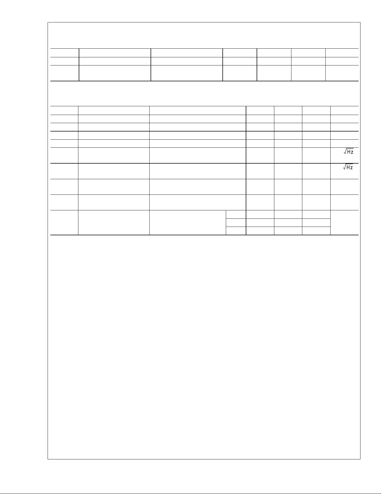
Symbol Parameter Conditions Min Typ Max Units
V
OS
Input Offset Voltage 0.8 25
35
Offset Calibration Time 0.5 10
12
TCV
Input Offset Voltage 0.015 µV/˚C
OS
Long-Term Offset Drift 0.006 µV/month
Lifetime V
I
IN
I
OS
R
IND
Input Current -3 pA
Input Offset Current 6 pA
Input Differential Resistance 9 MΩ
CMRR Common Mode Rejection
Ratio
PSRR Power Supply Rejection
Ratio
A
VOL
Open Loop Voltage Gain RL= 10kΩ 130 95
Drift 2.5 5 µV
OS
−0.3 ≤ V
0 ≤ V
CM
2.7V ≤ V
≤ 0.9V
CM
≤ 0.9V
+
≤ 5V 120 95
130 95
90
90
90
=2kΩ 124 90
R
L
85
V
O
Output Swing RL= 10kΩ to 1.35V
(diff) =±0.5V
V
IN
2.665
2.655
2.68
0.033 0.060
0.075
R
=2kΩ to 1.35V
L
(diff) =±0.5V
V
IN
2.630
2.615
2.65
0.061 0.085
0.105
I
O
R
OUT
I
S
Output Current Sourcing, VO=0V
(diff) =±0.5V
V
IN
Sinking, V
(diff) =±0.5V
V
IN
O
=5V
Output Impedance 0.05 Ω
Supply Current 0.919 1.20
12 5
18 5
3
mA
3
mA
1.50
+
µV
ms
dB
dB
dB
V
V
www.national.com 2

LMV2011
2.7V AC Electrical Characteristics T
>
1MΩ. Boldface limits apply at the temperature extremes.
= 25˚C, V+= 2.7V, V-= 0V, VCM= 1.35V, VO= 1.35V, and R
J
Symbol Parameter Conditions Min Typ Max Units
GBW Gain-Bandwidth Product 3 MHz
SR Slew Rate 4 V/µs
θ
m
G
m
e
n
Phase Margin 60 Deg
Gain Margin −14 dB
Input-Referred Voltage
35 nV/
Noise
i
n
Input-Referred Current
150 fA/
Noise
enp-p Input-Referred Voltage
RS= 100Ω, DC to 10Hz 850 nV
Noise
t
rec
Input Overload Recovery
50 ms
Time
t
s
Output Settling Time AV= −1, RL=2kΩ
1V Step
1% 0.9 µs
0.1% 49
0.01% 100
5V DC Electrical Characteristics Unless otherwise specified, all limits guaranteed for T
-
= 0V, VCM= 2.5V, VO= 2.5V and R
5V, V
>
1MΩ. Boldface limits apply at the temperature extremes.
L
= 25˚C, V+=
J
Symbol Parameter Conditions Min Typ Max Units
V
OS
Input Offset Voltage 0.12 25
µV
35
Offset Calibration Time 0.5 10
ms
12
TCV
Input Offset Voltage 0.015 µV/˚C
OS
Long-Term Offset Drift 0.006 µV/month
Lifetime V
I
IN
I
OS
R
IND
Input Current -3 pA
Input Offset Current 6 pA
Input Differential Resistance 9 MΩ
CMRR Common Mode Rejection
Ratio
PSRR Power Supply Rejection
Ratio
A
VOL
Open Loop Voltage Gain RL= 10kΩ 130 105
Drift 2.5 5 µV
OS
−0.3 ≤ V
0 ≤ V
CM
2.7V ≤ V
≤ 3.2
CM
≤ 3.2
+
≤ 5V 120 95
130 100
90
90
100
RL=2kΩ 132 95
dB
dB
dB
90
V
O
Output Swing RL= 10kΩ to 2.5V
(diff) =±0.5V
V
IN
4.96
4.95
4.978
0.040 0.070
V
0.085
R
=2kΩ to 2.5V
L
(diff) =±0.5V
V
IN
4.895
4.875
4.919
0.091 0.115
V
0.140
I
O
Output Current Sourcing, VO=0V
(diff) =±0.5V
V
IN
Sinking, V
(diff) =±0.5V
V
IN
O
=5V
15 8
17 8
6
mA
6
L
pp
www.national.com3
5V DC Electrical Characteristics Unless otherwise specified, all limits guaranteed for T
-
= 0V, VCM= 2.5V, VO= 2.5V and R
5V, V
>
1MΩ. Boldface limits apply at the temperature extremes. (Continued)
L
= 25˚C, V+=
J
LMV2011
Symbol Parameter Conditions Min Typ Max Units
R
OUT
I
S
Output Impedance 0.05 Ω
Supply Current per Channel 0.930 1.20
1.50
mA
5V AC Electrical Characteristics T
= 25˚C, V+= 5V, V-= 0V, VCM= 2.5V, VO= 2.5V, and R
J
>
L
1MΩ. Boldface limits apply at the temperature extremes.
Symbol Parameter Conditions Min Typ Max Units
GBW Gain-Bandwidth Product 3 MHz
SR Slew Rate 4 V/µs
θ
m
G
m
e
n
Phase Margin 60 deg
Gain Margin −15 dB
Input-Referred Voltage
35 nV/
Noise
i
n
Input-Referred Current
150 fA/
Noise
enp-p Input-Referred Voltage
RS= 100Ω, DC to 10Hz 850 nV
Noise
t
rec
Input Overload Recovery
50 ms
Time
t
s
Output Settling Time AV= −1, RL=2kΩ
1V Step
1% 0.8 us
0.1% 36
0.01% 100
Note 1: Absolute Maximum Ratings indicate limits beyond which damage may occur. Operating Ratings indicate conditions for which the device is intended to be
functional, but specific performance is not guaranteed. For guaranteed specifications and test conditions, see the Electrical Characteristics.
pp
www.national.com 4
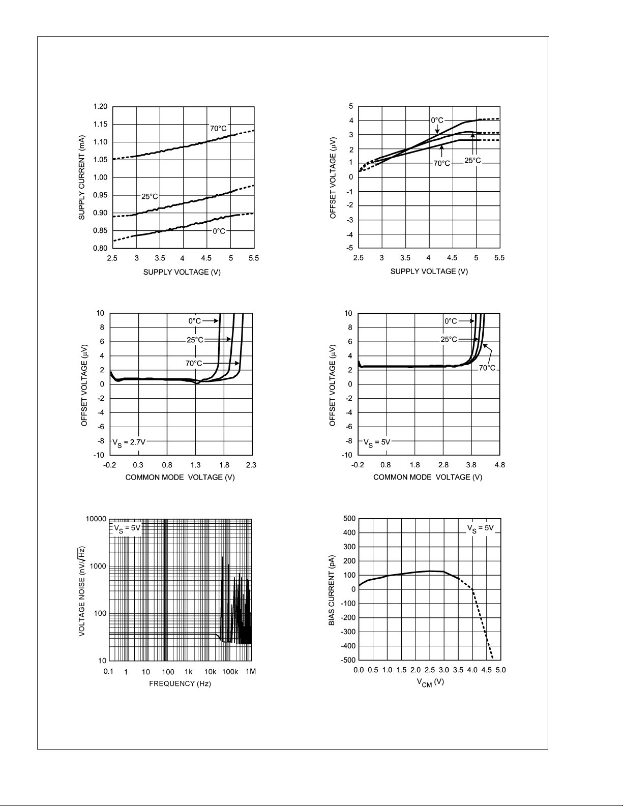
Typical Performance Characteristics
TA=25C, VS= 5V unless otherwise specified.
Supply Current vs. Supply Voltage Offset Voltage vs. Supply Voltage
LMV2011
20051524
Offset Voltage vs. Common Mode Offset Voltage vs. Common Mode
20051535 20051534
Voltage Noise vs. Frequency Input Bias Current vs. Common Mode
20051525
20051504
20051503
www.national.com5

Typical Performance Characteristics (Continued)
LMV2011
PSRR vs. Frequency PSRR vs. Frequency
20051507 20051506
Output Sourcing@2.7V Output Sourcing@5V
20051526
Output Sinking@2.7V Output Sinking@5V
20051528 20051529
www.national.com 6
20051527
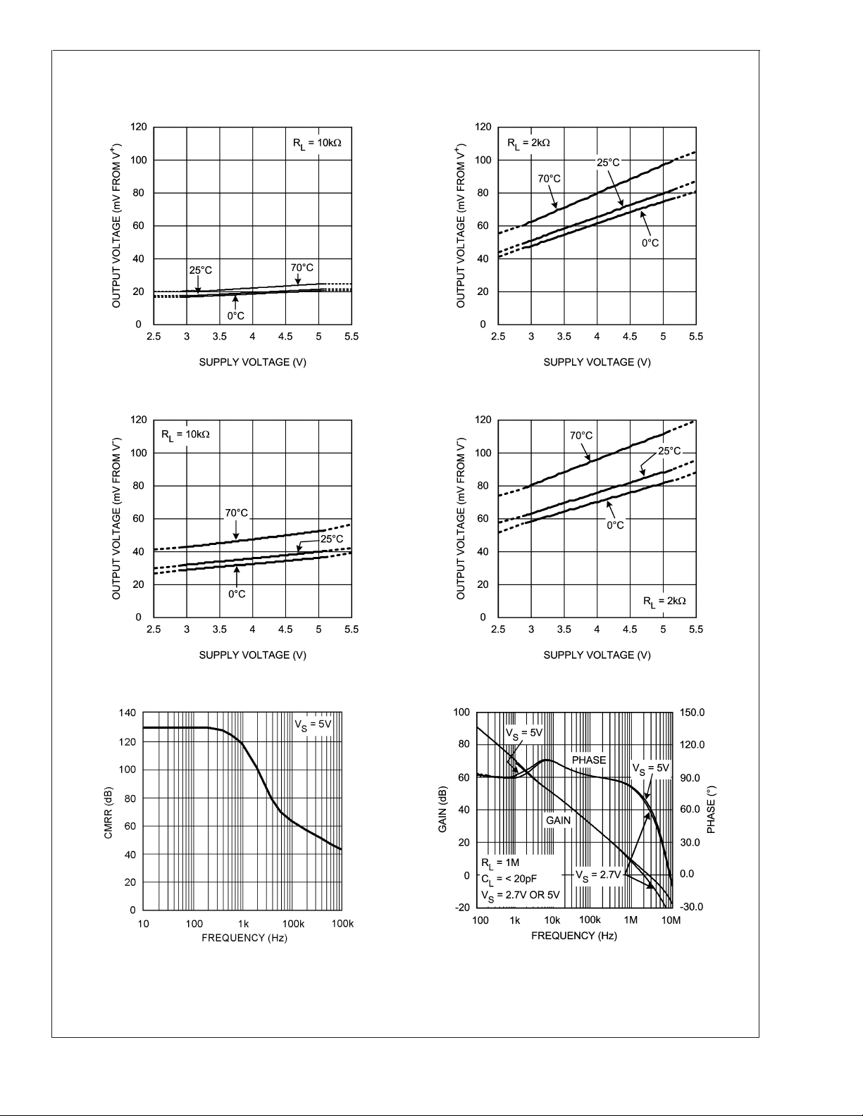
Typical Performance Characteristics (Continued)
Max Output Swing vs. Supply Voltage Max Output Swing vs. Supply Voltage
20051530 20051531
Min Output Swing vs. Supply Voltage Min Output Swing vs. Supply Voltage
LMV2011
20051532 20051533
CMRR vs. Frequency Open Loop Gain and Phase vs. Supply Voltage
20051505
20051508
www.national.com7

Typical Performance Characteristics (Continued)
LMV2011
Open Loop Gain and Phase vs. R
Open Loop Gain and Phase vs. C
@
2.7V Open Loop Gain and Phase vs. R
L
20051509 20051510
@
2.7V Open Loop Gain and Phase vs. C
L
@
5V
L
@
5V
L
20051511
20051512
Open Loop Gain and Phase vs. Temperature@2.7V Open Loop Gain and Phase vs. Temperature@5V
20051536 20051537
www.national.com 8
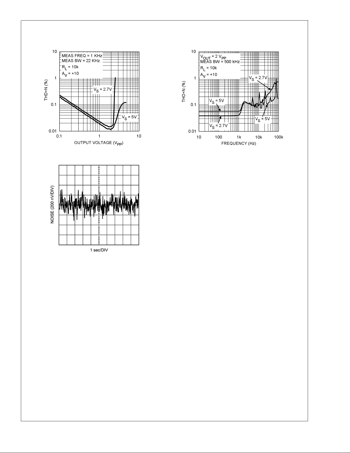
Typical Performance Characteristics (Continued)
THD+N vs. AMPL THD+N vs. Frequency
LMV2011
0.1Hz − 10Hz Noise vs. Time
20051514
20051515
20051513
www.national.com9

Application Information
THE BENEFITS OF LMV2011
LMV2011
NO 1/f NOISE
Using patented methods, the LMV2011 eliminates the 1/f
noise present in other amplifiers. That noise, which increases as frequency decreases, is a major source of measurement error in all DC-coupled measurements. Lowfrequency noise appears as a constantly-changing signal in
series with any measurement being made. As a result, even
when the measurement is made rapidly, this constantlychanging noise signal will corrupt the result. The value of this
noise signal can be surprisingly large. For example: If a
conventional amplifier has a flat-band noise level of 10nV/
and a noise corner of 10Hz, the RMS noise at 0.001Hz
is 1µV/
error, in the frequency range 0.001 Hz to 1.0 Hz. In a circuit
with a gain of 1000, this produces a 0.50mV peak-to-peak
output error. This number of 0.001 Hz might appear unreasonably low, but when a data acquisition system is operating
for 17 minutes, it has been on long enough to include this
error. In this same time, the LMV2011 will only have a
0.21mV output error. This is smaller by 2.4 x. Keep in mind
that this 1/f error gets even larger at lower frequencies. At the
extreme, many people try to reduce this error by integrating
or taking several samples of the same signal. This is also
doomed to failure because the 1/f nature of this noise means
that taking longer samples just moves the measurement into
lower frequencies where the noise level is even higher.
The LMV2011 eliminates this source of error. The noise level
is constant with frequency so that reducing the bandwidth
reduces the errors caused by noise.
Another source of error that is rarely mentioned is the error
voltage caused by the inadvertent thermocouples created
when the common "Kovar type" IC package lead materials
are soldered to a copper printed circuit board. These steelbased leadframe materials can produce over 35µV/˚C when
soldered onto a copper trace. This can result in thermocouple noise that is equal to the LMV2011 noise when there
is a temperature difference of only 0.0014˚C between the
lead and the board!
For this reason, the lead-frame of the LMV2011 is made of
copper. This results in equal and opposite junctions which
cancel this effect. The extremely small size of the SOT-23
package results in the leads being very close together. This
further reduces the probability of temperature differences
and hence decreases thermal noise.
OVERLOAD RECOVERY
The LMV2011 recovers from input overload much faster than
most chopper-stabilized opamps. Recovery from driving the
amplifier to 2X the full scale output, only requires about
40ms. Many chopper-stabilized amplifiers will take from
250ms to several seconds to recover from this same overload. This is because large capacitors are used to store the
unadjusted offset voltage.
. This is equivalent to a 0.50µV peak-to-peak
20051516
FIGURE 1.
The wide bandwidth of the LMV2011 enhances performance
when it is used as an amplifier to drive loads that inject
transients back into the output. ADCs (Analog-to-Digital Converters) and multiplexers are examples of this type of load.
To simulate this type of load, a pulse generator producing a
1V peak square wave was connected to the output through a
10pF capacitor. (Figure 1) The typical time for the output to
recover to 1% of the applied pulse is 80ns. To recover to
0.1% requires 860ns. This rapid recovery is due to the wide
bandwidth of the output stage and large total GBW.
NO EXTERNAL CAPACITORS REQUIRED
The LMV2011 does not need external capacitors. This eliminates the problems caused by capacitor leakage and dielectric absorption, which can cause delays of several seconds
from turn-on until the amplifier’s error has settled.
MORE BENEFITS
The LMV2011 offers the benefits mentioned above and
more. It has a rail-to-rail output and consumes only 950µA of
supply current while providing excellent DC and AC electrical
performance. In DC performance, the LMC2001 achieves
130dB of CMRR, 120dB of PSRR and 130dB of open loop
gain. In AC performance, the LMV2011 provides 3MHz of
gain-bandwidth product and 4V/µs of slew rate.
HOW THE LMV2011 WORKS
The LMV2011 uses new, patented techniques to achieve the
high DC accuracy traditionally associated with chopperstabilized amplifiers without the major drawbacks produced
by chopping. The LMV2011 continuously monitors the input
offset and corrects this error. The conventional chopping
process produces many mixing products, both sums and
differences, between the chopping frequency and the incoming signal frequency. This mixing causes large amounts of
distortion, particularly when the signal frequency approaches
the chopping frequency. Even without an incoming signal,
the chopper harmonics mix with each other to produce even
more trash. If this sounds unlikely or difficult to understand,
look at the plot (Figure 2), of the output of a typical (MAX432)
chopper-stabilized opamp. This is the output when there is
no incoming signal, just the amplifier in a gain of -10 with the
input grounded. The chopper is operating at about 150Hz;
the rest is mixing products. Add an input signal and the noise
gets much worse. Compare this plot with Figure 3 of the
LMV2011. This data was taken under the exact same conditions. The auto-zero action is visible at about 30kHz but
note the absence of mixing products at other frequencies. As
a result, the LMV2011 has very low distortion of 0.02% and
very low mixing products.
www.national.com 10

Application Information (Continued)
20051517
FIGURE 2.
LMV2011
PRECISION STRAIN-GAUGE AMPLIFIER
This Strain-Gauge amplifier (Figure 4) provides high gain
(1006 or~60 dB) with very low offset and drift. Using the
resistors’ tolerances as shown, the worst case CMRR will be
greater than 108 dB. The CMRR is directly related to the
resistor mismatch. The rejection of common-mode error, at
the output, is independent of the differential gain, which is
set by R3. The CMRR is further improved, if the resistor ratio
matching is improved, by specifying tighter-tolerance resistors, or by trimming.
20051518
20051504
FIGURE 3.
INPUT CURRENTS
The LMV2011’s input currents are different than standard
bipolar or CMOS input currents in that it appears as a current
flowing in one input and out the other. Under most operating
conditions, these currents are in the picoamp level and will
have little or no effect in most circuits. These currents tend to
increase slightly when the common-mode voltage is near the
minus supply. (See the typical curves.) At high temperatures
such as 85˚C, the input currents become larger, 0.5nA typical, and are both positive except when the V
is near V−.If
CM
operation is expected at low common-mode voltages and
high temperature, do not add resistance in series with the
inputs to balance the impedances. Doing this can cause an
increase in offset voltage. A small resistance such as 1kΩ
can provide some protection against very large transients or
overloads, and will not increase the offset significantly.
FIGURE 4.
Extending Supply Voltages and Output Swing by Using
a Composite Amplifier Configuration:
In cases where substantially higher output swing is required
with higher supply voltages, arrangements like the ones
shown in Figure 5 and Figure 6 could be used. These
configurations utilize the excellent DC performance of the
LMV2011 while at the same time allow the superior voltage
and frequency capabilities of the LM6171 to set the dynamic
performance of the overall amplifier. For example, it is pos-
±
sible to achieve
GBW (A
due to V
V
OS
12V output swing with 300MHz of overall
= 100) while keeping the worst case output shift
less than 4mV. The LMV2011 output voltage is
kept at about mid-point of its overall supply voltage, and its
input common mode voltage range allows the V- terminal to
be grounded in one case (Figure 5, inverting operation) and
tied to a small non-critical negative bias in another (Figure 6,
non-inverting operation). Higher closed-loop gains are also
possible with a corresponding reduction in realizable bandwidth. Table 1 shows some other closed loop gain possibilities along with the measured performance in each case.
www.national.com11

Application Information (Continued)
LMV2011
20051520
20051519
FIGURE 5.
TABLE 1. Composite Amplifier Measured Performance
AV R1
R2ΩC2pFBW
Ω
MHzSR(V/µs)
en p-p
(mV
PP
)
50 200 10k 8 3.3 178 37
100 100 10k 10 2.5 174 70
100 1k 100k 0.67 3.1 170 70
500 200 100k 1.75 1.4 96 250
1000 100 100k 2.2 0.98 64 400
In terms of the measured output peak-to-peak noise, the
following relationship holds between output noise voltage, e
p-p, for different closed-loop gain, AV, settings, where −3dB
Bandwidth is BW:
FIGURE 6.
It should be kept in mind that in order to minimize the output
noise voltage for a given closed-loop gain setting, one could
minimize the overall bandwidth. As can be seen from Equation 1 above, the output noise has a square-root relationship
to the Bandwidth.
In the case of the inverting configuration, it is also possible to
increase the input impedance of the overall amplifier, by
raising the value of R1, without having to increase the feedback resistor, R2, to impractical values, by utilizing a "Tee"
network as feedback. See the LMC6442 data sheet (Application Notes section) for more details on this.
n
FIGURE 7.
www.national.com 12
20051521

Application Information (Continued)
LMV2011 AS ADC INPUT AMPLIFIER
The LMV2011 is a great choice for an amplifier stage immediately before the input of an ADC (Analog-to-Digital Converter), whether AC or DC coupled. See Figure 7 and Figure
8. This is because of the following important characteristics:
A) Very low offset voltage and offset voltage drift over time
and temperature allow a high closed-loop gain setting
without introducing any short-term or long-term errors.
For example, when set to a closed-loop gain of 100 as
the analog input amplifier for a 12-bit A/D converter, the
overall conversion error over full operation temperature
and 30 years life of the part (operating at 50˚C) would be
less than 5 LSBs.
B) Fast large-signal settling time to 0.01% of final value
(1.4µs) allows 12 bit accuracy at 100KH
pling rate.
C) No flicker (1/f) noise means unsurpassed data accuracy
over any measurement period of time, no matter how
long. Consider the following opamp performance, based
on a typical low-noise, high-performance commerciallyavailable device, for comparison:
Opamp flatband noise = 8nV/
or more sam-
Z
1/f corner frequency = 100Hz
= 2000
A
V
Measurement time = 100 sec
Bandwidth = 2Hz
This example will result in about 2.2 mV
(1.9 LSB) of
PP
output noise contribution due to the opamp alone, compared to about 594µV
(less than 0.5 LSB) when that
PP
opamp is replaced with the LMV2011 which has no 1/f
contribution. If the measurement time is increased from
100 seconds to 1 hour, the improvement realized by
using the LMV2011 would be a factor of about 4.8 times
(2.86mV
compared to 596µV when LMV2011 is used)
PP
mainly because the LMV2011 accuracy is not compromised by increasing the observation time.
D) Copper leadframe construction minimizes any thermo-
couple effects which would degrade low level/high gain
data conversion application accuracy (see discussion
under "The Benefits of the LMV2011" section above).
E) Rail-to-Rail output swing maximizes the ADC dynamic
range in 5-Volt single-supply converter applications. Below are some typical block diagrams showing the
LMV2011 used as an ADC amplifier (Figure 7 and Figure
8).
LMV2011
FIGURE 8.
20051522
www.national.com13
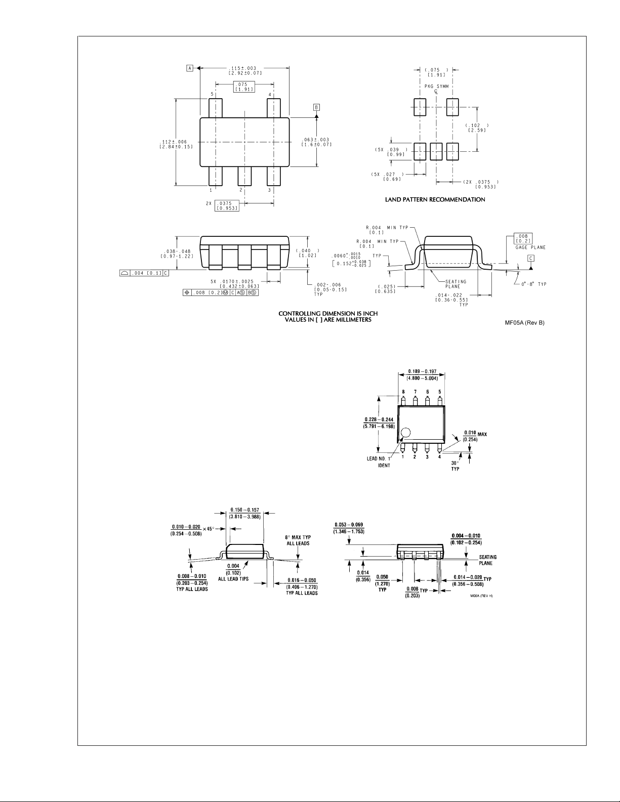
Physical Dimensions inches (millimeters) unless otherwise noted
LMV2011
5-Pin SOT23
NS Package Number MF0A5
8-Pin SOIC
NS Package Number M08A
www.national.com 14

Notes
LMV2011 High Precision, Rail-to-Rail Output Operational Amplifier
LIFE SUPPORT POLICY
NATIONAL’S PRODUCTS ARE NOT AUTHORIZED FOR USE AS CRITICAL COMPONENTS IN LIFE SUPPORT
DEVICES OR SYSTEMS WITHOUT THE EXPRESS WRITTEN APPROVAL OF THE PRESIDENT AND GENERAL
COUNSEL OF NATIONAL SEMICONDUCTOR CORPORATION. As used herein:
1. Life support devices or systems are devices or
systems which, (a) are intended for surgical implant
into the body, or (b) support or sustain life, and
whose failure to perform when properly used in
accordance with instructions for use provided in the
2. A critical component is any component of a life
support device or system whose failure to perform
can be reasonably expected to cause the failure of
the life support device or system, or to affect its
safety or effectiveness.
labeling, can be reasonably expected to result in a
significant injury to the user.
BANNED SUBSTANCE COMPLIANCE
National Semiconductor certifies that the products and packing materials meet the provisions of the Customer Products
Stewardship Specification (CSP-9-111C2) and the Banned Substances and Materials of Interest Specification
(CSP-9-111S2) and contain no ‘‘Banned Substances’’ as defined in CSP-9-111S2.
National Semiconductor
Americas Customer
Support Center
Email: new.feedback@nsc.com
Tel: 1-800-272-9959
www.national.com
National does not assume any responsibility for use of any circuitry described, no circuit patent licenses are implied and National reserves the right at any time without notice to change said circuitry and specifications.
National Semiconductor
Europe Customer Support Center
Fax: +49 (0) 180-530 85 86
Email: europe.support@nsc.com
Deutsch Tel: +49 (0) 69 9508 6208
English Tel: +44 (0) 870 24 0 2171
Français Tel: +33 (0) 1 41 91 8790
National Semiconductor
Asia Pacific Customer
Support Center
Email: ap.support@nsc.com
National Semiconductor
Japan Customer Support Center
Fax: 81-3-5639-7507
Email: jpn.feedback@nsc.com
Tel: 81-3-5639-7560
 Loading...