


LMV1032-06/LMV1032-15/LMV1032-25
Amplifiers for 3 Wire Analog Electret Microphones
LMV1032-06/LMV1032-15/LMV1032-25 Amplifiers for 3 Wire Analog Electret Microphones
February 2004
General Description
The LMV1032 is an audio amplifier series for small form
factor electret microphones. It is designed to replace the
JFET preamp currently being used. The LMV1032 series is
ideal for extended battery life applications, such as a bluetooth communication link. The addition of a third pin in
electret microphones that incorporate the LMV1032 allows
for a dramatic reduction in supply current as compared to the
JFET equipped electret microphone. Microphone supply current is thus reduced to 60 µA, assuring longer battery life.
The LMV1032 series is guaranteed for supply voltages from
1.7V to 5V, and has fixed voltage gains of 6 dB, 15 dB and 25
dB.
The LMV1032 series offers low output impedance over the
voice bandwidth, excellent power supply rejection (PSRR),
and stability over temperature.
The devices are offered in space saving 4-bump ultra thin
micro SMD (TM) lead free package and are thus ideally
suited for the form factor of miniature electret microphone
packages.
Block Diagram
Features
(Typical LMV1032-06, 1.7V Supply; Unless Otherwise
Noted)
n Output voltage noise (A-weighted) −97 dBV
n Low supply current 60 µA
n Supply voltage 1.7V to 5V
n PSRR 84 dB
n Signal to noise ratio 58 dB
n Input capacitance 2 pF
n Input impedance
n Output impedance
n Max input signal 300 mV
n Temperature range −40˚C to 85˚C
n Offered in 1.13 x 1.13 x 0.4mm Ultra Thin micro SMD
lead free (NOPB) package
>
100 MΩ
<
200Ω
PP
Applications
n Mobile communications - Bluetooth
n Automotive accessories
n Cellular phones
n PDAs
n Accessory microphone products
Electret Microphone
20084202
20084201
© 2004 National Semiconductor Corporation DS200842 www.national.com
Absolute Maximum Ratings (Note 1)
If Military/Aerospace specified devices are required,
please contact the National Semiconductor Sales Office/
Distributors for availability and specifications.
Storage Temperature Range −65˚C to 150˚C
Junction Temperature (Note 6) 150˚C max
Mounting Temperature
Infrared or Convection (20 sec.) 235˚C
ESD Tolerance (Note 2)
Human Body Model 2500V
Operating Ratings (Note 1)
Machine Model 250V
Supply Voltage
- GND 5.5V
V
DD
Supply Voltage 1.7V to 5V
Temperature Range −40˚C to +85˚C
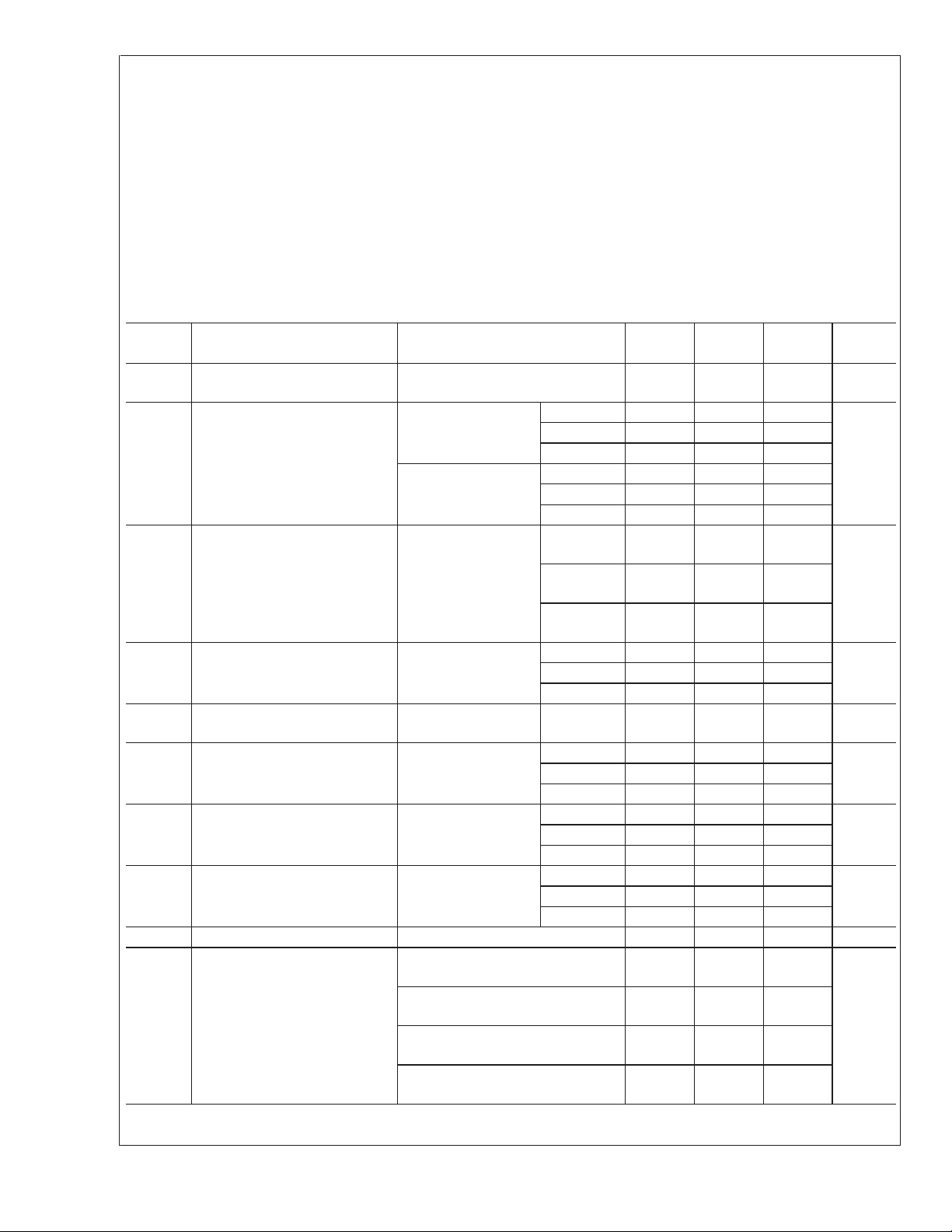
1.7V and 5V Electrical Characteristics (Note 3)
Unless otherwise specified, all limits guaranteed for TJ= 25˚C and VDD= 1.7V and 5V. Boldface limits apply at the temperature extremes.
LMV1032-06/LMV1032-15/LMV1032-25
Symbol Parameter Conditions
I
DD
SNR Signal to Noise Ratio VDD= 1.7V
PSRR Power Supply Rejection Ratio 1.7V
V
IN
f
LOW
f
HIGH
e
n
V
OUT
R
O
I
O
Supply Current VIN= GND 60 85
=18mV
V
IN
f=1kHz
=5V
V
DD
=18mV
V
IN
f=1kHz
<
V
DD
Max Input Signal f = 1kHz and THD+N
<
1%
Lower −3 dB Roll Off Frequency R
Upper −3 dB Roll Off Frequency R
SOURCE
V
IN
SOURCE
V
IN
=50Ω
=18mV
=50Ω
=18mV
Output Noise A-Weighted LMV1032-06 −97
Output Voltage VIN= GND LMV1032-06 100 300 500
Output Impedance f=1kHz
Output Current VDD= 1.7V, V
VDD= 1.7V, V
= 5V, V
V
DD
V
DD
= 5V, V
OUT
OUT
LMV1032-06 58
PP
LMV1032-15 61
LMV1032-25 61
LMV1032-06 59
PP
LMV1036-15 61
LMV1032-25 62
<
5V LMV1032-06 65
LMV1032-15 60
LMV1032-25 55
LMV1032-06 300
LMV1032-15 170
LMV1032-25 60
PP
LMV1032-06 120
PP
LMV1032-25 21
LMV1032-25 −80
LMV1032-25 300 600 1000
= 1.7V, Sinking 0.9
OUT
= 0V, Sourcing 0.3
OUT
= 1.7V, Sinking 0.9
= 0V, Sourcing 0.4
Min
(Note 4)
60
55
50
0.5
0.2
0.5
0.1
Typ
(Note 5)
Max
(Note 4) Units
100
75
70
65
70
<
200 Ω
2.3
0.64
2.4
1.46
mV
kHzLMV1032-15 75
dBVLMV1032-15 −89
mVLMV1032-15 250 500 750
mA
µA
dB
dB
PP
Hz
www.national.com 2

1.7V and 5V Electrical Characteristics (Note 3) (Continued)
Unless otherwise specified, all limits guaranteed for TJ= 25˚C and VDD= 1.7V and 5V. Boldface limits apply at the temperature extremes.
Min
Symbol Parameter Conditions
THD Total Harmonic Distortion f=1kHz
=18mV
V
IN
PP
LMV1032-06 0.11
(Note 4)
LMV1032-25 0.35
C
IN
Z
IN
A
V
Input Capacitance 2pF
Input Impedance
Gain f=1kHz
=18mV
V
IN
PP
LMV1032-06 5.5
4.5
LMV1032-15 14.8
14
LMV1032-25 24.8
24
Note 1: Absolute Maximum Ratings indicate limits beyond which damage to the device may occur. Operating Ratings indicate conditions for which the device is
intended to be functional, but specific performance is not guaranteed. For guaranteed specifications and the test conditions, see the Electrical Characteristics.
Note 2: Human Body Model (HBM) is 1.5 kΩ in series with 100 pF.
Note 3: Electrical Table values apply only for factory testing conditions at the temperature indicated. Factory testing conditions result in very limited self-heating of
the device such that T
Note 4: All limits are guaranteed by design or statistical analysis.
Note 5: Typical values represent the most likely parametric norm.
Note 6: The maximum power dissipation is a function of T
(T
J(MAX)-TA
)/θJA. All numbers apply for packages soldered directly into a PC board.
. No guarantee of parametric performance is indicated in the electrical tables under conditions of internal self-heating where T
J=TA
, θJAand TA. The maximum allowable power dissipation at any ambient temperature is PD=
J(MAX)
Typ
(Note 5)
>
100 MΩ
Max
(Note 4) Units
6.2 6.7
7.7
15.4 16
17
25.5 26.2
27
LMV1032-06/LMV1032-15/LMV1032-25
%LMV1032-15 0.13
dB
>
TA.
J
www.national.com3

Connection Diagram
4-Bump Ultra Thin micro SMD
LMV1032-06/LMV1032-15/LMV1032-25
Note: - Pin numbers are referenced to package marking text orientation.
- The actual physical placement of the package marking will vary slightly from part to part. The package will designate the date code and will vary considerably.
Package marking does not correlate to device type in any way.
Ordering Information
Package Part Number Package Marking Transport Media NSC Drawing
LMV1032UP-06
LMV1032UPX-06 3k Units Tape and Reel
4-Bump Ultra Thin
micro SMD lead free
Note: The LMV1032 series is offered only with lead free (NOPB) solder bumps.
The LMV1032 series replaces the LMV1014.
LMV1032UP-15
LMV1032UPX-15 3k Units Tape and Reel
LMV1032UP-25
LMV1032UPX-25 3k Units Tape and Reel
Top View
Date Code
Date Code
Date Code
20084203
250 Units Tape and Reel
250 Units Tape and Reel
250 Units Tape and Reel
UPA04QQA
www.national.com 4

LMV1032-06/LMV1032-15/LMV1032-25
Typical Performance Characteristics Unless otherwise specified, V
= 1.7V, single supply, TA=
S
25˚C
Supply Current vs. Supply Voltage (LMV1032-06) Supply Current vs. Supply Voltage (LMV1032-15)
20084204
Closed Loop Gain and Phase vs. Frequency
Supply Current vs. Supply Voltage (LMV1032-25)
(LMV1032-06)
20084213
20084214
Closed Loop Gain and Phase vs. Frequency
(LMV1032-15)
20084215
20084205
Closed Loop Gain and Phase vs. Frequency
(LMV1032-25)
20084216
www.national.com5

Typical Performance Characteristics Unless otherwise specified, V
25˚C (Continued)
= 1.7V, single supply, TA=
S
Power Supply Rejection Ratio vs. Frequency
(LMV1036-06)
LMV1032-06/LMV1032-15/LMV1032-25
Power Supply Rejection Ratio vs. Frequency
(LMV1032-25) Total Harmonic Distortion vs. Frequency (LMV1032-06)
20084206
Power Supply Rejection Ratio vs. Frequency
(LMV1032-15)
20084217
20084218
Total Harmonic Distortion vs. Frequency (LMV1032-15) Total Harmonic Distortion vs. Frequency (LMV1032-25)
20084219
www.national.com 6
20084207
20084220

LMV1032-06/LMV1032-15/LMV1032-25
Typical Performance Characteristics Unless otherwise specified, V
25˚C (Continued)
Total Harmonic Distortion vs. Input Voltage
(LMV1032-06)
20084208
Total Harmonic Distortion vs. Input Voltage
(LMV1032-25) Output Voltage Noise vs. Frequency (LMV1032-06)
Total Harmonic Distortion vs. Input Voltage
(LMV1032-15)
= 1.7V, single supply, TA=
S
20084221
20084222
20084223
Output Voltage Noise vs. Frequency (LMV1032-15) Output Voltage Noise vs. Frequency (LMV1032-25)
20084224 20084225
www.national.com7

Application Section
LOW CURRENT
The LMV1032 has low supply current for a longer battery life.
The low supply current makes this amplifier suitable for
microphone applications which need to be always on.
BUILT IN GAIN
The LMV1032 is offered in space saving small micro SMD
package in order to fit in the metal can of a microphone. The
LMV1032 is placed on the PCB inside the microphone.
The bottom side of the PCB has the pins that connect the
supply voltage to the amplifier and make the output available. The input of the amplifier is connected inside the metal
can via the PCB to the microphone.
LMV1032-06/LMV1032-15/LMV1032-25
20084209
FIGURE 2. A-Weighted Filter
MEASURING NOISE AND SNR
The overall noise of the LMV1032 is measured within the
frequency band from 10 Hz to 22 kHz using an A-weighted
filter. The input of the LMV1032 is connected to ground with
a 5 pF capacitor.
20084202
FIGURE 1. Built-in Gain
A-WEIGHTED FILTER
The human ear has a frequency range from 20 Hz to about
20 kHz. Within this range the sensitivity of the human ear is
not equal for each frequency. To approach the hearing response weighting filters are introduced. One of those filters
is the A-weighted filter.
The A-weighted filter is usually used in signal to noise ratio
measurements, where sound is compared to device noise. It
improves the correlation of the measured data to the signal
to noise ratio perceived by the human ear.
20084210
FIGURE 3. Noise Measurement Setup
Signal to noise ratio (SNR) is measured with a 1 kHz input
signal of 18 mV
using an A-weighted filter. This represents
PP
a sound pressure level of 94 dB SPL. No input capacitor is
connected.
SOUND PRESSURE LEVEL
The volume of sound applied to a microphone is usually
stated as a pressure level referred to the threshold of hearing of the human ear. The sound pressure level (SPL) in
decibels is defined by:
Sound pressure level (dB) = 20 log P
m/PO
Where,
is the measured sound pressure
P
m
P
is the threshold of hearing (20µPa)
O
In order to be able to calculate the resulting output voltage of
the microphone for a given SPL, the sound pressure in dB
SPL needs to be converted to the absolute sound pressure
in dBPa. This is the sound pressure level in decibels referred
to 1 Pascal (Pa).
www.national.com 8

Application Section (Continued)
The conversion is given by:
dBPa = dB SPL + 20*log 20 µPa
dBPa=dBSPL-94dB
Translation from absolute sound pressure level to a voltage
is specified by the sensitivity of the microphone. A conventional microphone has a sensitivity of −44 dBV/Pa.
LMV1032-06/LMV1032-15/LMV1032-25
20084212
FIGURE 5. Gain vs. Frequency Over Temperature
The LMV1032 is optimized to be used in audio band applications. By using the LMV1032, the gain response is flat
within the audio band and has the linearity and temperature
stability.
20084211
FIGURE 4. dB SPL to dBV Conversion
Example: Busy traffic is 70 dB SPL
= 70 −94 −44 = −68 dBV
V
OUT
This is equivalent to 1.13 mV
PP
Since the LMV1032-06 has a gain of 2 (6 dB) over the JFET,
the output voltage of the microphone is 2.26 mV
PP
.By
implementing the LMV1032-06, the sensitivity of the microphone is −38 dBV/Pa (−44 + 6).
LOW FREQUENCY CUT OFF FILTER
To reduce noise on the output of the microphone a low cut
filter has been implemented. This filter reduces the effect of
wind and handling noise.
It’s also helpful to reduce the proximity effect in directional
microphones. This effect occurs when the sound source is
very close to the microphone. The lower frequencies are
amplified which gives a bass sound. This amplification can
cause an overload, which results in a distortion of the signal.
ADVANTAGE OF THREE PINS
The LMV1032 has three pins instead of two pins as in the
case of a JFET solution. The third pin brings the advantage
of a low supply current, high PSRR and eliminates the need
for additional components.
Noise pick-up by a microphone in a cell phone is a wellknown problem. A conventional JFET circuit is sensitive for
noise pick-up because of its high output impedance. The
output impedance is usually around 2.2 kΩ. By separating
the output pin and the positive supply pin a much lower
output impedance is achieved. The output of the LMV1032 is
therefore less sensitive to noise pick-up.
RF noise is amongst other caused by non-linear behavior.
The non-linear behavior of the amplifier at high frequencies,
well above the usable bandwidth of the device, causes AMdemodulation of high frequency signals. The AM modulation
contained in such signals folds back into the audio band,
thereby disturbing the intended microphone signal. The
GSM signal of a cell phone is such an AM-modulated signal.
The modulation frequency of 216 Hz and its harmonics can
be observed in the audio band. This kind of noise is called
bumblebee noise.
www.national.com9

Physical Dimensions inches (millimeters)
unless otherwise noted
LMV1032-06/LMV1032-15/LMV1032-25
NOTE: UNLESS OTHERWISE SPECIFIED.
1. TITANIUM COATING.
2. FOR SOLDER BUMP COMPOSITION, SEE "SOLDER INFORMATION" IN THE PACKAGING SECTION OF THE NATIONAL SEMICONDUCTOR WEB
PAGE (www.national.com).
3. RECOMMEND NON-SOLDER MASK DEFINED LANDING PAD.
4. PIN A1 IS ESTABLISHED BY LOWER LEFT CORNER WITH RESPECT TO TEXT ORIENTATION.
5. XXX IN DRAWING NUMBER REPRESENTS PACKAGE SIZE VARIATION WHERE X1 IS PACKAGE WIDTH, X2 IS PACKAGE LENGTH AND X3 IS
PACKAGE HEIGHT.
6. REFERENCE JEDEC REGISTRATION MO-211. VARIATION BC.
4-Bump Ultra Thin micro SMD
NS Package Number UPA04QQA
X1 = 1.133mm X2 = 1.133mm X3 = 0.4mm
www.national.com 10

Notes
LMV1032-06/LMV1032-15/LMV1032-25 Amplifiers for 3 Wire Analog Electret Microphones
LIFE SUPPORT POLICY
NATIONAL’S PRODUCTS ARE NOT AUTHORIZED FOR USE AS CRITICAL COMPONENTS IN LIFE SUPPORT
DEVICES OR SYSTEMS WITHOUT THE EXPRESS WRITTEN APPROVAL OF THE PRESIDENT AND GENERAL
COUNSEL OF NATIONAL SEMICONDUCTOR CORPORATION. As used herein:
1. Life support devices or systems are devices or
systems which, (a) are intended for surgical implant
into the body, or (b) support or sustain life, and
whose failure to perform when properly used in
accordance with instructions for use provided in the
2. A critical component is any component of a life
support device or system whose failure to perform
can be reasonably expected to cause the failure of
the life support device or system, or to affect its
safety or effectiveness.
labeling, can be reasonably expected to result in a
significant injury to the user.
BANNED SUBSTANCE COMPLIANCE
National Semiconductor certifies that the products and packing materials meet the provisions of the Customer Products
Stewardship Specification (CSP-9-111C2) and the Banned Substances and Materials of Interest Specification
(CSP-9-111S2) and contain no ‘‘Banned Substances’’ as defined in CSP-9-111S2.
National Semiconductor
Americas Customer
Support Center
Email: new.feedback@nsc.com
Tel: 1-800-272-9959
www.national.com
National does not assume any responsibility for use of any circuitry described, no circuit patent licenses are implied and National reserves the right at any time without notice to change said circuitry and specifications.
National Semiconductor
Europe Customer Support Center
Fax: +49 (0) 180-530 85 86
Email: europe.support@nsc.com
Deutsch Tel: +49 (0) 69 9508 6208
English Tel: +44 (0) 870 24 0 2171
Français Tel: +33 (0) 1 41 91 8790
National Semiconductor
Asia Pacific Customer
Support Center
Email: ap.support@nsc.com
National Semiconductor
Japan Customer Support Center
Fax: 81-3-5639-7507
Email: jpn.feedback@nsc.com
Tel: 81-3-5639-7560
 Loading...