


查询LMV1012供应商
LMV1012 Analog Series:
Pre-Amplified IC’s for High Gain 2-Wire Microphones
LMV1012 Analog Series Pre-Amplified IC’s for High Gain 2-Wire Microphones
August 2004
General Description
The LMV1012 is an audio amplifier series for small form
factor electret microphones. This 2-wire portfolio is designed
to replace the JFET amplifier currently being used. The
LMV1012 series is ideally suited for applications requiring
high signal integrity in the presence of ambient or RF noise,
such as in cellular communications. The LMV1012 audio
amplifiers are guaranteed to operate over a 2.2V to 5.0V
supply voltage range with fixed gains of 7.8 dB, 15.6 dB,
20.9 dB, and 23.8 dB. The devices offer excellent THD, gain
accuracy and temperature stability as compared to a JFET
microphone.
The LMV1012 series enables a two-pin electret microphone
solution, which provides direct pin-to-pin compatibility with
the existing JFET market.
The devices are offered in extremely thin space saving
4-bump micro SMD packages. The LMV1012XP is designed
for 1.0 mm canisters and thicker ECM canisters. These
extremely miniature packages are designed for electret condenser microphones (ECM) form factor.
Schematic Diagram
Features
(Typical LMV1012-15, 2.2V supply, RL= 2.2 kΩ, C = 2.2 µF,
=18mVPP, unless otherwise specified)
V
IN
n Supply voltage 2V - 5V
n Supply current
n Signal to noise ratio (A-weighted) 60 dB
n Output voltage noise (A-weighted) −89 dBV
n Total harmonic distortion 0.09%
n Voltage gain
— LMV1012-07 7.8 dB
— LMV1012-15 15.6 dB
— LMV1012-20 20.9 dB
— LMV1012-25 23.8 dB
n Temperature range −40˚C to 85˚C
n Offered in 4-bump micro SMD packages
<
180 µA
Applications
n Cellular phones
n Headsets
n Mobile communications
n Automotive accessories
n PDAs
n Accessory microphone products
Built-In Gain Electret Microphone
20058702
20058701
© 2004 National Semiconductor Corporation DS200587 www.national.com

Absolute Maximum Ratings (Note 1)
If Military/Aerospace specified devices are required,
please contact the National Semiconductor Sales Office/
Distributors for availability and specifications.
Storage Temperature Range −65˚C to 150˚C
Junction Temperature (Note 6) 150˚C max
Mounting Temperature
Infrared or Convection (20 sec.) 235˚C
ESD Tolerance (Note 2)
Human Body Model 2500V
Operating Ratings (Note 1)
Machine Model 250V
LMV1012 Analog Series
Supply Voltage
- GND 5.5V
V
DD
Supply Voltage 2V to 5V
Temperature Range −40˚C to 85˚C
2.2V Electrical Characteristics (Note 3)
Unless otherwise specified, all limits guaranteed for TJ= 25˚C, VDD= 2.2V, VIN= 18 mV, RL= 2.2 kΩ and C = 2.2 µF.
Boldface limits apply at the temperature extremes.
Symbol Parameter Conditions
I
DD
SNR Signal to Noise Ratio f = 1 kHz, V
Supply Current VIN= GND LMV1012-07 139 250
=18
IN
mV, A-Weighted
V
V
f
LOW
f
HIGH
e
IN
OUT
n
Max Input Signal f = 1 kHz and
<
THD+N
1%
Output Voltage VIN= GND LMV1012-07 1.65
Lower −3dB Roll Off Frequency R
Upper −3dB Roll Off Frequency R
SOURCE
SOURCE
=50Ω 65 Hz
=50Ω 95 kHz
Output Noise A-Weighted LMV1012-07 −96
THD Total Harmonic Distortion f = 1 kHz,
V
=18mV
IN
C
IN
Z
IN
Input Capacitance 2pF
Input Impedance
Min
(Note 4)
LMV1012-15 180 300
LMV1012-20 160 250
LMV1012-25 141 250
LMV1012-07 59
LMV1012-15 60
LMV1012-20 61
LMV1012-25 61
LMV1012-07 170
LMV1012-15 100
LMV1012-20 50
LMV1012-25 28
1.54
LMV1012-15 1.54
1.48
LMV1012-20 1.65
1.55
LMV1012-25 1.65
1.49
LMV1012-15 −89
LMV1012-20 −84
LMV1012-25 −82
LMV1012-07 0.10
LMV1012-15 0.09
LMV1012-20 0.12
LMV1012-25 0.15
Typ
(Note 5)
1.90 2.03
1.81 1.94
1.85 2.03
1.90 2.02
>
1000 GΩ
Max
(Note 4) Units
300
325
µA
300
300
dB
mV
PP
2.09
2.00
V
2.13
2.18
dBV
%
www.national.com 2

2.2V Electrical Characteristics (Note 3) (Continued)
Unless otherwise specified, all limits guaranteed for TJ= 25˚C, VDD= 2.2V, VIN= 18 mV, RL= 2.2 kΩ and C = 2.2 µF.
Boldface limits apply at the temperature extremes.
Symbol Parameter Conditions
A
V
Gain f = 1 kHz,
R
SOURCE
=50Ω
Min
(Note 4)
LMV1012-07 6.4
5.5
LMV1012-15 14.0
13.1
LMV1012-20 19.5
17.4
LMV1012-25 22.5
21.4
Typ
(Note 5)
(Note 4) Units
7.8 9.5
15.6 16.9
20.9 22.0
23.8 25.0
Max
10.0
17.5
23.3
25.7
5V Electrical Characteristics (Note 3)
Unless otherwise specified, all limits guaranteed for TJ= 25˚C, VDD= 5V, VIN= 18 mV, RL= 2.2 kΩ and C = 2.2 µF.
Boldface limits apply at the temperature extremes.
Symbol Parameter Conditions
I
DD
SNR Signal to Noise Ratio f = 1 kHz, V
Supply Current VIN= GND LMV1012-07 158 250
=18
IN
mV, A-Weighted
V
V
f
LOW
f
HIGH
e
IN
OUT
n
Max Input Signal f = 1 kHz and
<
THD+N
1%
Output Voltage VIN= GND LMV1012-07 4.45
Lower −3dB Roll Off Frequency R
Upper −3dB Roll Off Frequency R
SOURCE
SOURCE
=50Ω 67 Hz
=50Ω 150 kHz
Output Noise A-Weighted LMV1012-07 −96
THD Total Harmonic Distortion f = 1 kHz,
V
=18mV
IN
Min
(Note 4)
LMV1012-15 200 300
LMV1012-20 188 260
LMV1012-25 160 250
LMV1012-07 59
LMV1012-15 60
LMV1012-20 61
LMV1012-25 61
LMV1012-07 170
LMV1012-15 100
LMV1012-20 55
LMV1012-25 28
4.38
LMV1012-15 4.34
4.28
LMV1012-20 4.40
4.30
LMV1012-25 4.45
4.39
LMV1012-15 −89
LMV1012-20 −84
LMV1012-25 −82
LMV1012-07 0.12
LMV1012-15 0.13
LMV1012-20 0.18
LMV1012-25 0.21
Typ
(Note 5)
(Note 4) Units
4.65 4.80
4.56 4.74
4.58 4.75
4.65 4.83
Max
300
325
310
300
4.85
4.80
4.85
4.86
mV
dBV
LMV1012 Analog Series
dB
µA
dB
PP
V
%
www.national.com3

5V Electrical Characteristics (Note 3) (Continued)
Unless otherwise specified, all limits guaranteed for TJ= 25˚C, VDD= 5V, VIN= 18 mV, RL= 2.2 kΩ and C = 2.2 µF.
Boldface limits apply at the temperature extremes.
Min
Symbol Parameter Conditions
C
IN
Z
IN
A
V
LMV1012 Analog Series
Input Capacitance 2pF
Input Impedance
Gain f = 1 kHz,
R
SOURCE
=50Ω
LMV1012-07 6.4
(Note 4)
5.5
LMV1012-15 14.0
13.1
LMV1012-20 19.2
17.0
LMV1012-25 22.5
21.2
Note 1: Absolute Maximum Ratings indicate limits beyond which damage to the device may occur. Operating Ratings indicate conditions for which the device is
intended to be functional, but specific performance is not guaranteed. For guaranteed specifications and the test conditions, see the Electrical Characteristics.
Note 2: Human Body Model (HBM) is 1.5 kΩ in series with 100 pF.
Note 3: Electrical Table values apply only for factory testing conditions at the temperature indicated. Factory testing conditions result in very limited self-heating of
the device such that T
Note 4: All limits are guaranteed by design or statistical analysis.
Note 5: Typical values represent the most likely parametric norm.
Note 6: The maximum power dissipation is a function of T
P
=(T
D
J(MAX)-TA
. No guarantee of parametric performance is indicated in the electrical tables under conditions of internal self-heating where T
J=TA
, θJAand TA. The maximum allowable power dissipation at any ambient temperature is
)/θJA. All numbers apply for packages soldered directly into a PC board.
J(MAX)
Typ
(Note 5)
>
1000 GΩ
Max
(Note 4) Units
8.1 9.5
10.7
15.6 16.9
17.5
21.1 22.3
23.5
23.9 25.0
25.8
dB
>
TA.
J
www.national.com 4

Connection Diagram
LMV1012 Analog Series
4-Bump micro SMD
Top View
Note: - Pin numbers are referenced to package marking text orientation.
- The actual physical placement of the package marking will vary slightly from part to part. The package will designate the date code and will vary considerably.
Package marking does not correlate to device type in any way.
20058703
Ordering Information
Package Part Number Package Marking Transport Media NSC Drawing
4-Bump Extreme Thin
micro SMD
(0.3 mm max height)
lead free only
4-Bump Ultra-Thin
micro SMD
(0.4 mm max height)
lead free only
4-Bump Thin
micro SMD
(0.5 mm max height)
LMV1012XP-15
LMV1012XPX-15 3k Units Tape and Reel
LMV1012XP-25 250 Units Tape and Reel
LMV1012XPX-25 3k Units Tape and Reel
LMV1012UP-07
LMV1012UPX-07 3k Units Tape and Reel
LMV1012UP-15 250 Units Tape and Reel
LMV1012UPX-15 3k Units Tape and Reel
LMV1012UP-20 250 Units Tape and Reel
LMV1012UPX-20 3k Units Tape and Reel
LMV1012UP-25 250 Units Tape and Reel
LMV1012UPX-25 3k Units Tape and Reel
LMV1012TP-07
LMV1012TPX-07 3k Units Tape and Reel
LMV1012TP-15 250 Units Tape and Reel
LMV1012TPX-15 3k Units Tape and Reel
LMV1012TP-25 250 Units Tape and Reel
LMV1012TPX-25 3k Units Tape and Reel
Date Code
Date Code
Date Code
250 Units Tape and Reel
XPA04HLA
250 Units Tape and Reel
UPA04GKA
250 Units Tape and Reel
TPA04GKA
www.national.com5
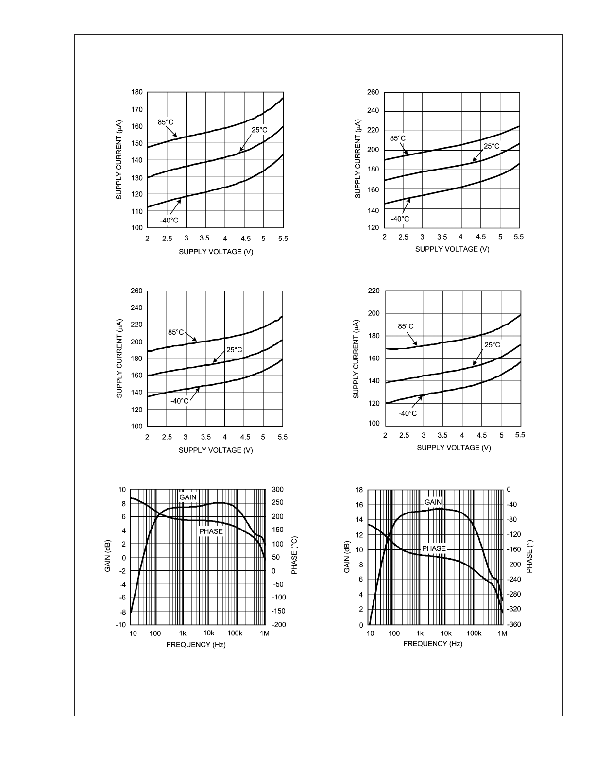
Typical Performance Characteristics Unless otherwise specified, V
C = 2.2 µF, single supply, T
Supply Current vs. Supply Voltage (LMV1012-07) Supply Current vs. Supply Voltage (LMV1012-15)
LMV1012 Analog Series
= 25˚C
A
= 2.2V, RL= 2.2 kΩ,
S
20058718
20058704
Supply Current vs. Supply Voltage (LMV1012-20) Supply Current vs. Supply Voltage (LMV1012-25)
20058724
20058719
Gain and Phase vs. Frequency (LMV1012-07) Gain and Phase vs. Frequency (LMV1012-15)
20058714
www.national.com 6
20058705

LMV1012 Analog Series
Typical Performance Characteristics Unless otherwise specified, V
C = 2.2 µF, single supply, T
= 25˚C (Continued)
A
= 2.2V, RL= 2.2 kΩ,
S
Gain and Phase vs. Frequency (LMV1012-20) Gain and Phase vs. Frequency (LMV1012-25)
20058725 20058713
Total Harmonic Distortion vs. Frequency (LMV1012-07) Total Harmonic Distortion vs. Frequency (LMV1012-15)
20058720
20058706
Total Harmonic Distortion vs. Frequency (LMV1012-20) Total Harmonic Distortion vs. Frequency (LMV1012-25)
20058726 20058721
www.national.com7

Typical Performance Characteristics Unless otherwise specified, V
C = 2.2 µF, single supply, T
= 25˚C (Continued)
A
= 2.2V, RL= 2.2 kΩ,
S
LMV1012 Analog Series
Total Harmonic Distortion vs. Input Voltage
(LMV1012-07)
20058722
Total Harmonic Distortion vs. Input Voltage
(LMV1012-20)
Total Harmonic Distortion vs. Input Voltage
(LMV1012-15)
20058707
Total Harmonic Distortion vs. Input Voltage
(LMV1012-25)
20058727 20058723
Output Noise vs. Frequency (LMV1012-07) Output Noise vs. Frequency (LMV1012-15)
20058717
www.national.com 8
20058715
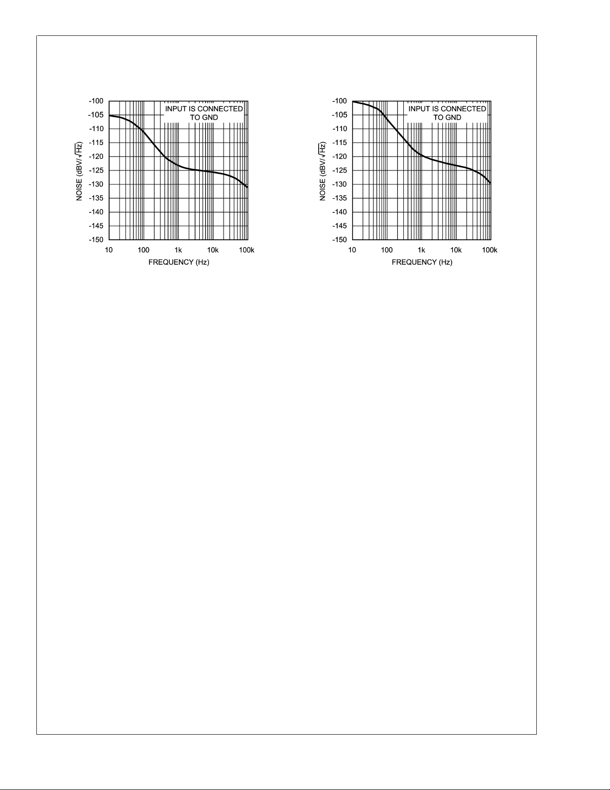
LMV1012 Analog Series
Typical Performance Characteristics Unless otherwise specified, V
C = 2.2 µF, single supply, T
Output Noise vs. Frequency (LMV1012-20) Output Noise vs. Frequency (LMV1012-25)
= 25˚C (Continued)
A
20058728 20058716
= 2.2V, RL= 2.2 kΩ,
S
www.national.com9

Application Section
HIGH GAIN
The LMV1012 series provides outstanding gain versus the
JFET and still maintains the same ease of implementation,
with improved gain, linearity and temperature stability. A high
gain eliminates the need for extra external components.
BUILT IN GAIN
LMV1012 Analog Series
The LMV1012 is offered in 0.3 mm height space saving
small 4-pin micro SMD packages in order to fit inside the
different size ECM canisters of a microphone. The LMV1012
is placed on the PCB inside the microphone.
The bottom side of the PCB usually shows a bull’s eye
pattern where the outer ring, which is shorted to the metal
can, should be connected to the ground. The center dot on
the PCB is connected to the V
phantom biasing allows both supply voltage and output signal on one connection.
through a resistor. This
DD
20058709
FIGURE 2. A-Weighted Filter
MEASURING NOISE AND SNR
The overall noise of the LMV1012 is measured within the
frequency band from 10 Hz to 22 kHz using an A-weighted
filter. The input of the LMV1012 is connected to ground with
a 5 pF capacitor, as in Figure 3. Special precautions in the
internal structure of the LMV1012 have been taken to reduce
the noise on the output.
20058702
FIGURE 1. Built in Gain
A-WEIGHTED FILTER
The human ear has a frequency range from 20 Hz to about
20 kHz. Within this range the sensitivity of the human ear is
not equal for each frequency. To approach the hearing response weighting filters are introduced. One of those filters
is the A-weighted filter.
The A-weighted filter is usually used in signal to noise ratio
measurements, where sound is compared to device noise.
This filter improves the correlation of the measured data to
the signal to noise ratio perceived by the human ear.
20058710
FIGURE 3. Noise Measurement Setup
The signal to noise ratio (SNR) is measured witha1kHz
input signal of 18 mV
using an A-weighted filter. This
PP
represents a sound pressure level of 94 dB SPL. No input
capacitor is connected for the measurement.
SOUND PRESSURE LEVEL
The volume of sound applied to a microphone is usually
stated as a pressure level referred to the threshold of hearing of the human ear. The sound pressure level (SPL) in
decibels is defined by:
Sound pressure level (dB) = 20 log P
m/PO
Where,
is the measured sound pressure
P
m
P
is the threshold of hearing (20 µPa)
O
In order to be able to calculate the resulting output voltage of
the microphone for a given SPL, the sound pressure in dB
www.national.com 10

Application Section (Continued)
SPL needs to be converted to the absolute sound pressure
in dBPa. This is the sound pressure level in decibels referred
to 1 Pascal (Pa).
The conversion is given by:
dBPa = dB SPL + 20*log 20 µPa
dBPa=dBSPL-94dB
Translation from absolute sound pressure level to a voltage
is specified by the sensitivity of the microphone. A conventional microphone has a sensitivity of -44 dBV/Pa.
LMV1012 Analog Series
amplified which gives a bass sound. This amplification can
cause an overload, which results in a distortion of the signal.
20058712
FIGURE 5. LMV1012-15 Gain vs. Frequency Over
Temperature
The LMV1012 is optimized to be used in audio band applications. By using the LMV1012, the gain response is flat
within the audio band and has linearity and temperature
stability Figure 5.
20058711
FIGURE 4. dB SPL to dBV Conversion
Example: Busy traffic is 70 dB SPL
= 70 −94 −44 = −68 dBV
V
OUT
This is equivalent to 1.13 mV
PP
Since the LMV1012-15 has a gain of 6 (15.6 dB) over the
JFET, the output voltage of the microphone is 6.78 mV
.By
PP
implementing the LMV1012-15, the sensitivity of the microphone is -28.4 dBV/Pa (−44 + 15.6).
LOW FREQUENCY CUT OFF FILTER
To reduce noise on the output of the microphone a low
frequency cut off filter has been implemented. This filter
reduces the effect of wind and handling noise.
It’s also helpful to reduce the proximity effect in directional
microphones. This effect occurs when the sound source is
very close to the microphone. The lower frequencies are
NOISE
Noise pick-up by a microphone in cell phones is a wellknown problem. A conventional JFET circuit is sensitive for
noise pick-up because of its high output impedance, which is
usually around 2.2 kΩ.
RF noise is amongst other caused by non-linear behavior.
The non-linear behavior of the amplifier at high frequencies,
well above the usable bandwidth of the device, causes AMdemodulation of high frequency signals. The AM modulation
contained in such signals folds back into the audio band,
thereby disturbing the intended microphone signal. The
GSM signal of a cell phone is such an AM-modulated signal.
The modulation frequency of 216 Hz and its harmonics can
be observed in the audio band. This kind of noise is called
bumblebee noise.
RF noise caused by a GSM signal can be reduced by
connecting two external capacitors to ground, see Figure 6.
One capacitor reduces the noise caused by the 900 MHz
carrier and the other reduces the noise caused by 1800/
1900 MHz.
www.national.com11

Application Section (Continued)
LMV1012 Analog Series
20058708
FIGURE 6. RF Noise Reduction
www.national.com 12

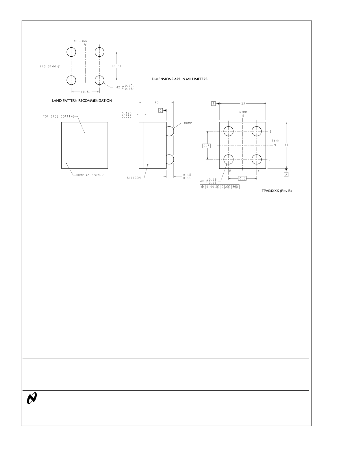
Physical Dimensions inches (millimeters) unless otherwise noted
LMV1012 Analog Series
NOTE: UNLESS OTHERWISE SPECIFIED.
1. FOR SOLDER BUMP COMPOSITION, SEE "SOLDER INFORMATION" IN THE PACKAGING SECTION OF THE NATIONAL SEMICONDUCTOR WEB
PAGE (www.national.com).
2. RECOMMEND NON-SOLDER MASK DEFINED LANDING PAD.
3. PIN A1 IS ESTABLISHED BY LOWER LEFT CORNER WITH RESPECT TO TEXT ORIENTATION.
4. XXX IN DRAWING NUMBER REPRESENTS PACKAGE SIZE VARIATION WHERE X1 IS PACKAGE WIDTH, X2 IS PACKAGE LENGTH AND X3 IS
PACKAGE HEIGHT.
5. REFERENCE JEDEC REGISTRATION MO-211. VARIATION CA.
4-Bump Extreme Thin micro SMD
NS Package Number XPA04HLA
= 0.955 mm X2= 1.031 mm X3= 0.300 mm
X
1
www.national.com13

Physical Dimensions inches (millimeters) unless otherwise noted (Continued)
LMV1012 Analog Series
NOTE: UNLESS OTHERWISE SPECIFIED.
1. TITANIUM COATING.
2. FOR SOLDER BUMP COMPOSITION, SEE "SOLDER INFORMATION" IN THE PACKAGING SECTION OF THE NATIONAL SEMICONDUCTOR WEB
PAGE (www.national.com).
3. RECOMMEND NON-SOLDER MASK DEFINED LANDING PAD.
4. PIN A1 IS ESTABLISHED BY LOWER LEFT CORNER WITH RESPECT TO TEXT ORIENTATION.
5. XXX IN DRAWING NUMBER REPRESENTS PACKAGE SIZE VARIATION WHERE X1 IS PACKAGE WIDTH, X2 IS PACKAGE LENGTH AND X3 IS
PACKAGE HEIGHT.
6. REFERENCE JEDEC REGISTRATION MO-211. VARIATION CA.
4-Bump ULTRA-Thin micro SMD
NS Package Number UPA04GKA
= 0.93 mm X2= 1.006 mm X3= 0.400 mm
X
1
www.national.com 14
Physical Dimensions inches (millimeters) unless otherwise noted (Continued)
LMV1012 Analog Series Pre-Amplified IC’s for High Gain 2-Wire Microphones
NOTE: UNLESS OTHERWISE SPECIFIED.
1. EPOXY COATING.
2. 63Sn/37Pb EUTECTIC BUMP.
3. RECOMMEND NON-SOLDER MASK DEFINED LANDING PAD.
4. PIN A1 IS ESTABLISHED BY LOWER LEFT CORNER WITH RESPECT TO TEXT ORIENTATION PINS ARE NUMBERED COUNTERCLOCKWISE.
5. XXX IN DRAWING NUMBER REPRESENTS PACKAGE SIZE VARIATION WHERE X1 IS PACKAGE WIDTH, X2 IS PACKAGE LENGTH AND X3 IS
PACKAGE HEIGHT.
6. REFERENCE JEDEC REGISTRATION MO-211. VARIATION BC.
4-Bump Thin micro SMD
NS Package Number TPA04GKA
= 0.93 mm X2= 1.006 mm X3= 0.500 mm
X
1
LIFE SUPPORT POLICY
NATIONAL’S PRODUCTS ARE NOT AUTHORIZED FOR USE AS CRITICAL COMPONENTS IN LIFE SUPPORT
DEVICES OR SYSTEMS WITHOUT THE EXPRESS WRITTEN APPROVAL OF THE PRESIDENT AND GENERAL
COUNSEL OF NATIONAL SEMICONDUCTOR CORPORATION. As used herein:
1. Life support devices or systems are devices or
systems which, (a) are intended for surgical implant
into the body, or (b) support or sustain life, and
whose failure to perform when properly used in
accordance with instructions for use provided in the
2. A critical component is any component of a life
support device or system whose failure to perform
can be reasonably expected to cause the failure of
the life support device or system, or to affect its
safety or effectiveness.
labeling, can be reasonably expected to result in a
significant injury to the user.
BANNED SUBSTANCE COMPLIANCE
National Semiconductor certifies that the products and packing materials meet the provisions of the Customer Products
Stewardship Specification (CSP-9-111C2) and the Banned Substances and Materials of Interest Specification
(CSP-9-111S2) and contain no ‘‘Banned Substances’’ as defined in CSP-9-111S2.
National Semiconductor
Americas Customer
Support Center
Email: new.feedback@nsc.com
Tel: 1-800-272-9959
www.national.com
National does not assume any responsibility for use of any circuitry described, no circuit patent licenses are implied and National reserves the right at any time without notice to change said circuitry and specifications.
National Semiconductor
Europe Customer Support Center
Fax: +49 (0) 180-530 85 86
Email: europe.support@nsc.com
Deutsch Tel: +49 (0) 69 9508 6208
English Tel: +44 (0) 870 24 0 2171
Français Tel: +33 (0) 1 41 91 8790
National Semiconductor
Asia Pacific Customer
Support Center
Email: ap.support@nsc.com
National Semiconductor
Japan Customer Support Center
Fax: 81-3-5639-7507
Email: jpn.feedback@nsc.com
Tel: 81-3-5639-7560
 Loading...