

August 2007
LMP7732
2.9 nV/sqrt(Hz) Low Noise, Precision, RRIO Amplifier
General Description
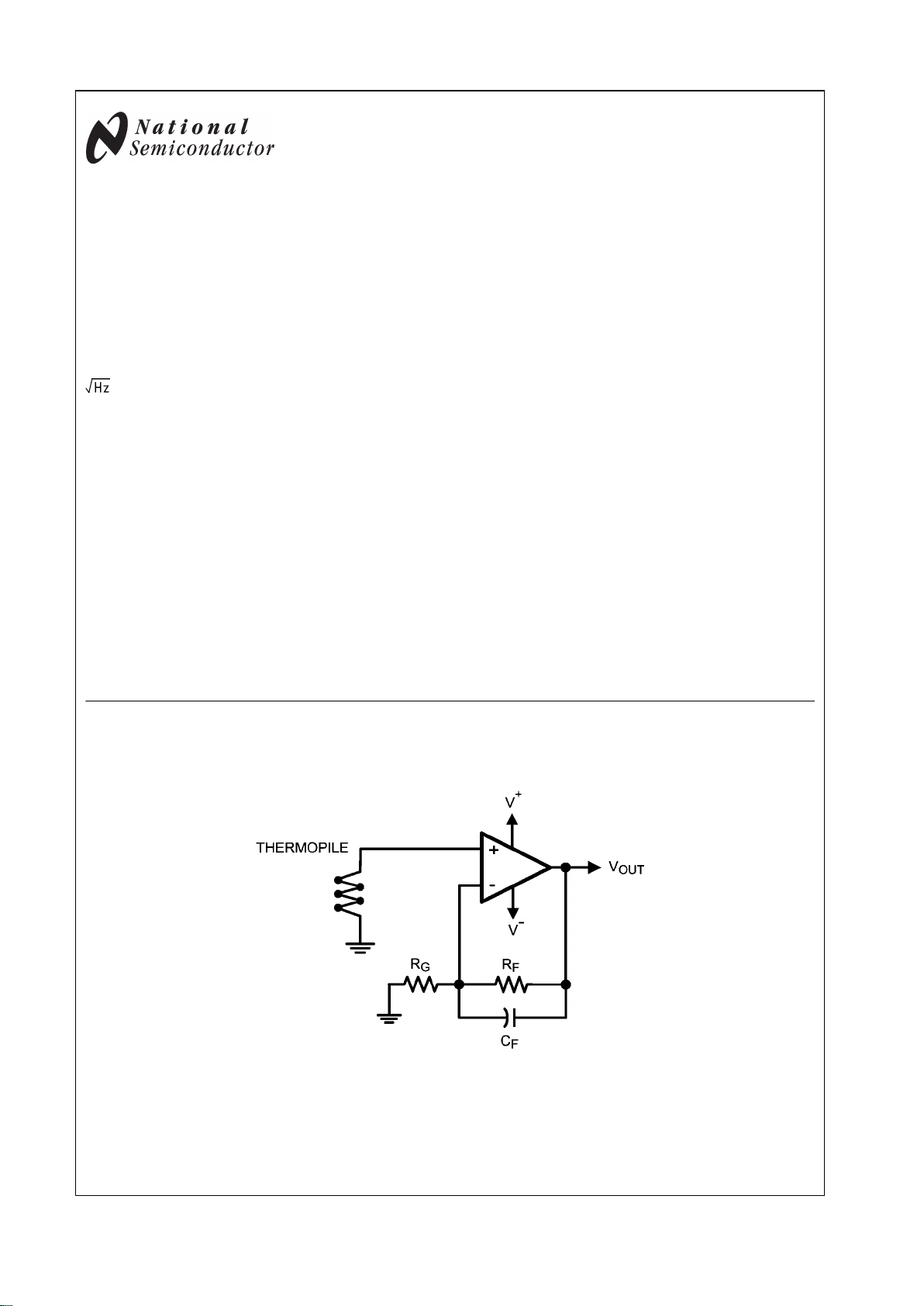
The LMP7732 is a dual low noise, low offset voltage, rail-torail input and output, low voltage precision amplifier. The
LMP7732 is part of the LMP® precision amplifier family and is
ideal for precision and low noise applications with low voltage
requirements.
This operational amplifier offers low voltage noise of 2.9 nV/
with a 1/f corner of only 3 Hz and low DC offset with a
maximum value of ±40 µV, targeting high accuracy, low frequency applications. The LMP7732 has bipolar junction input
stages with a bias current of only 1.5 nA. This low input bias
current, complemented by the very low AC and DC levels of
voltage noise, makes the LMP7732 an excellent choice for
photometry applications.
The LMP7732 provides a wide GBW of 22 MHz while consuming only 4 mA of current. This high gain bandwidth along
with the high open loop gain of 130 dB enables accurate signal conditioning in applications with high closed loop gain
requirements.
The LMP7732 has a supply voltage range of 1.8V to 5.5V,
making it an ideal choice for battery operated portable applications.
The LMP7732 is offered in an 8-pin SOIC.
The LMP7731 is the single version of this product and is of-
fered in an 5-Pin SOT23 package.
Features
(Typical values, TA = 25°C, VS = 5V)
■
Input voltage noise
—
f = 3 Hz 3.3 nV/√Hz
—
f = 1 kHz 2.9 nV/√Hz
■
Offset voltage (max) ±40 µV
■
Offset voltage drift (max) ±1.3 µV/°C
■
CMRR 130 dB
■
Open loop gain 130 dB
■
GBW 22 MHz
■
Slew rate 2.4 V/µs
■
THD @ f = 10 kHz, AV = 1, RL = 2 kΩ 0.001%
■
Supply current 4.4 mA
■
Supply voltage range 1.8V to 5.5V
■
Operating temperature range −40°C to 125°C
■
Input bias current ±1.5 nA
■
RRIO
■
8-Pin SOIC package
Applications
■
Thermopile amplifier
■
Gas analysis instruments
■
Photometric instrumentation
■
Medical instrumentation
Typical Application
Thermopile Signal Amplifier
30015001
LMP® is a registered trademark of National Semiconductor Corporation.
© 2007 National Semiconductor Corporation 300150 www.national.com
LMP7732 Low Noise, Precision, RRIO Amplifier
Absolute Maximum Ratings (Note 1)
If Military/Aerospace specified devices are required,
please contact the National Semiconductor Sales Office/
Distributors for availability and specifications.
ESD Tolerance (Note 2)
Human Body Model
For inputs pins only 2000V
For all other pins 2000V
Machine Model 200V
Charge Device Model 1000V
VIN Differential
±2V
Supply Voltage (VS = V+ – V−)
6.0V
Storage Temperature Range −65°C to 150°C
Junction Temperature (Note 3) +150°C max
Soldering Information
Infrared or Convection (20 sec) 235°C
Wave Soldering Lead Temp. (10 sec) 260°C
Operating Ratings (Note 1)
Temperature Range −40°C to 125°C
Supply Voltage (VS = V+ – V–)
1.8V to 5.5V
Package Thermal Resistance (θJA)
8-Pin SOIC 190 °C/W
2.5V Electrical Characteristics (Note 4)
Unless otherwise specified, all limits are guaranteed for TA = 25°C, V+ = 2.5V, V− = 0V, VCM = V+/2, RL >10 kΩ to V+/2. Boldface limits apply at the temperature extremes.
Symbol Parameter Conditions Min
(Note 6)
Typ
(Note 5)
Max
(Note 6)
Units
V
OS
Input Offset Voltage
(Note 7)
VCM = 2.0V ±9 ±50
±150
μV
VCM = 0.5V ±9 ±40
±125
TCV
OS
Input Offset Voltage Drift VCM = 2.0V ±0.5 ±1.3
μV/°C
VCM = 0.5V ±0.2 ±0.8
Input Offset Voltage Time Drift VCM = 0.5V and VCM = 2.0V 0.35
μV/month
I
B
Input Bias Current VCM = 2.0V ±1 ±30
±45
nA
VCM = 0.5V ±12 ±50
±75
I
OS
Input Offset Current VCM = 2.0V ±1 ±50
±75
nA
VCM = 0.5V ±11 ±60
±80
TCI
OS
Input Offset Current Drift VCM = 0.5V and VCM = 2.0V 0.0474 nA/°C
CMRR Common Mode Rejection Ratio
0.15V ≤ VCM ≤ 0.7V
0.23V ≤ VCM ≤ 0.7V
101
89
120
dB
1.5V ≤ VCM ≤ 2.35V
1.5V ≤ VCM ≤ 2.27V
105
99
129
PSRR Power Supply Rejection Ratio
2.5V ≤ V+ ≤ 5V
111
105
129
dB
1.8V ≤ V+ ≤ 5.5V
117
CMVR Input Common-Mode Voltage
Range
Large Signal CMRR ≥ 80 dB
0
2.5 V
A
VOL
Large Signal Voltage Gain
RL = 10 kΩ to V+/2
VO = 0.5V to 2.0V
112
104
130
dB
RL = 2 kΩ to V+/2
VO = 0.5V to 2.0V
109
90
119
www.national.com 2
LMP7732
Symbol Parameter Conditions Min
(Note 6)
Typ
(Note 5)
Max
(Note 6)
Units
V
O
Output Swing High
RL = 10 kΩ to V+/2
4 50
75
mV
from either
rail
RL = 2 kΩ to V+/2
13 50
75
Output Swing Low
RL = 10 kΩ to V+/2
6 50
75
RL = 2 kΩ to V+/2
9 50
75
I
O
Output Short Circuit Current Sourcing, VO = V+/2
VIN (diff) = 100 mV
22
12
31
mA
Sinking, VO = V+/2
VIN (diff) = −100 mV
15
10
44
I
S
Supply Current VCM = 2.0V 4.0 5.4
6.8
mA
VCM = 0.5V 4.6 6.2
7.8
SR Slew Rate
AV = +1, CL = 10 pF, RL = 10 kΩ to V+/2
VO = 2 V
PP
2.4
V/μs
GBW Gain Bandwidth Product
CL = 20 pF, RL = 10 kΩ to V+/2
21 MHz
G
M
Gain Margin
CL = 20 pF, RL = 10 kΩ to V+/2
14 dB
Φ
M
Phase Margin
CL = 20 pF, RL = 10 kΩ to V+/2
60 deg
R
IN
Input Resistance Differential Mode 38
kΩ
Common Mode 151
MΩ
THD Total Harmonic Distortion AV = 1, fO = 1 kHz, Amplitude = 1V 0.002
%
e
n
Input-Referred Voltage Noise f = 1 kHz, VCM = 2.0V 3.0
nV/
f = 1 kHz, VCM = 0.5V 3.0
0.1 Hz to 10 Hz 75 nV
PP
i
n
Input-Referred Current Noise f = 1 kHz, VCM = 2.0V 1.1
pA/
f = 1 kHz, VCM = 0.5V 2.3
3.3V Electrical Characteristics (Note 4)
Unless otherwise specified, all limits are guaranteed for TA = 25°C, V+ = 3.3V, V− = 0V, VCM = V+/2, RL > 10 kΩ to V+/2. Boldface limits apply at the temperature extremes.
Symbol Parameter Conditions Min
(Note 6)
Typ
(Note 5)
Max
(Note 6)
Units
V
OS
Input Offset Voltage
(Note 7)
VCM = 2.5V ±6 ±50
±150
μV
VCM = 0.5V ±6 ±40
±125
TCV
OS
Input Offset Voltage Drift VCM = 2.5V ±0.5 ±1.3
μV/°C
VCM = 0.5V ±0.2 ±0.8
Input Offset Voltage Time Drift VCM = 0.5V and VCM = 2.5V 0.35
μV/month
I
B
Input Bias Current VCM = 2.5V ±1.5 ±30
±45
nA
VCM = 0.5V ±13 ±50
±77
I
OS
Input Offset Current VCM = 2.5V ±1 ±50
±70
nA
VCM = 0.5V ±11 ±60
±80
3 www.national.com
LMP7732

Symbol Parameter Conditions Min
(Note 6)
Typ
(Note 5)
Max
(Note 6)
Units
TCI
OS
Input Offset Current Drift VCM = 0.5V and VCM = 2.5V 0.048 nA/°C
CMRR Common Mode Rejection Ratio
0.15V ≤ VCM ≤ 0.7V
0.23V ≤ VCM ≤ 0.7V
101
89
120
dB
1.5V ≤ VCM ≤ 3.15V
1.5V ≤ VCM ≤ 3.07V
105
99
130
PSRR Power Supply Rejection Ratio
2.5V ≤ V+ ≤ 5.0V
111
105
129
dB
1.8V ≤ V+ ≤ 5.5V
117
CMVR Input Common-Mode Voltage
Range
Large Signal CMRR ≥ 80 dB
0
3.3 V
A
VOL
Large Signal Voltage Gain
RL = 10 kΩ to V+/2
VO = 0.5V to 2.8V
112
104
130
dB
RL = 2 kΩ to V+/2
VO = 0.5V to 2.8V
110
92
119
V
O
Output Swing High
RL = 10 kΩ to V+/2
5 50
75
mV
from either
rail
RL = 2 kΩ to V+/2
14 50
75
Output Swing Low
RL = 10 kΩ to V+/2
9 50
75
RL = 2 kΩ to V+/2
13 50
75
I
O
Output Short Circuit Current Sourcing, VO = V+/2
VIN (diff) = 100 mV
28
22
45
mA
Sinking, VO = V+/2
VIN (diff) = −100 mV
25
20
48
I
S
Supply Current VCM = 2.5V 4.2 5.6
7.0
mA
VCM = 0.5V 4.8 6.4
8.0
SR Slew Rate
AV = +1, CL = 10 pF, RL = 10 kΩ to V+/2
VO = 2 V
PP
2.4
V/μs
GBW Gain Bandwidth Product
CL = 20 pF, RL = 10 kΩ to V+/2
22 MHz
G
M
Gain Margin
CL = 20 pF, RL = 10 kΩ to V+/2
14 dB
Φ
M
Phase Margin
CL = 20 pF, RL = 10 kΩ to V+/2
62 deg
THD Total Harmonic Distortion AV = 1, fO = 1 kHz, Amplitude = 1V 0.002
%
R
IN
Input Resistance Differential Mode 38
kΩ
Common Mode 151
MΩ
e
n
Input-Referred Voltage Noise f = 1 kHz, VCM = 2.5V
2.9
nV/
f = 1 kHz, VCM = 0.5V
2.9
0.1 Hz to 10 Hz 75 nV
PP
i
n
Input-Referred Current Noise f = 1 kHz, VCM = 2.5V 1.1
pA/
f = 1 kHz, VCM = 0.5V 2.1
www.national.com 4
LMP7732

5V Electrical Characteristics (Note 4)
Unless otherwise specified, all limits are guaranteed for TA = 25°C, V+ = 5V, V− = 0V, VCM = V+/2, RL > 10 kΩ to V+/2. Boldface
limits apply at the temperature extremes.
Symbol Parameter Conditions Min
(Note 6)
Typ
(Note 5)
Max
(Note 6)
Units
V
OS
Input Offset Voltage
(Note 7)
VCM = 4.5V ±6 ±50
±150
μV
VCM = 0.5V ±6 ±40
±125
TCV
OS
Input Offset Voltage Drift VCM = 4.5V ±0.5 ±1.3
μV/°C
VCM = 0.5V ±0.2 ±0.8
Input Offset Voltage Time Drift VCM = 0.5V and VCM = 4.5V 0.35
μV/month
I
B
Input Bias Current VCM = 4.5V ±1.5 ±30
±50
nA
VCM = 0.5V ±14 ±50
±85
I
OS
Input Offset Current VCM = 4.5V ±1 ±50
±70
nA
VCM = 0.5V ±11 ±65
±80
TCI
OS
Input Offset Current Drift VCM = 0.5V and VCM = 4.5V 0.0482 nA/°C
CMRR Common Mode Rejection Ratio
0.15V ≤ VCM ≤ 0.7V
0.23V ≤ VCM ≤ 0.7V
101
89
120
dB
1.5V ≤ VCM ≤ 4.85V
1.5V ≤ VCM ≤ 4.77V
105
99
130
PSRR Power Supply Rejection Ratio
2.5V ≤ V+ ≤ 5V
111
105
129
dB
1.8V ≤ V+ ≤ 5.5V
117
CMVR Input Common-Mode Voltage
Range
Large Signal CMRR ≥ 80 dB
0
5 V
A
VOL
Large Signal Voltage Gain
RL = 10 kΩ to V+/2
VO = 0.5V to 4.5V
112
104
130
dB
RL = 2 kΩ to V+/2
VO = 0.5V to 4.5V
110
94
119
V
O
Output Swing High
RL = 10 kΩ to V+/2
8 50
75
mV
from either
rail
RL = 2 kΩ to V+/2
24 50
75
Output Swing Low
RL = 10 kΩ to V+/2
9 50
75
RL = 2 kΩ to V+/2
23 50
75
I
O
Output Short Circuit Current Sourcing, VO = V+/2
VIN (diff) = 100 mV
33
27
47
mA
Sinking, VO = V+/2
VIN (diff) = −100 mV
30
25
49
I
S
Supply Current VCM = 4.5V 4.4 6.0
7.4
mA
VCM = 0.5V 5.0 6.8
8.4
SR Slew Rate
AV = +1, CL = 10 pF, RL = 10 kΩ to V+/2
VO = 2 V
PP
2.4
V/μs
5 www.national.com
LMP7732
Symbol Parameter Conditions Min
(Note 6)
Typ
(Note 5)
Max
(Note 6)
Units
GBW Gain Bandwidth Product
CL = 20 pF, RL = 10 kΩ to V+/2
22 MHz
G
M
Gain Margin
CL = 20 pF, RL = 10 kΩ to V+/2
12 dB
Φ
M
Phase Margin
CL = 20 pF, RL = 10 kΩ to V+/2
65 deg
R
IN
Input Resistance Differential Mode 38
kΩ
Common Mode 151
MΩ
THD Total Harmonic Distortion AV = 1, fO = 1 kHz, Amplitude = 1V 0.001
%
e
n
Input-Referred Voltage Noise f = 1 kHz, VCM = 4.5V
2.9
nV/
f = 1 kHz, VCM = 0.5V
2.9
0.1 Hz to 10 Hz 75 nV
PP
i
n
Input-Referred Current Noise f = 1 kHz, VCM = 4.5V
1.1
pA/
f = 1 kHz, VCM = 0.5V
2.2
Note 1: Absolute Maximum Ratings indicate limits beyond which damage to the device may occur. Operating Ratings indicate conditions for which the device is
intended to be functional, but specific performance is not guaranteed. For guaranteed specifications and the test conditions, see the Electrical Characteristics
Tables.
Note 2: Human Body Model, applicable std. MIL-STD-883, Method 3015.7. Machine Model, applicable std. JESD22-A115-A (ESD MM std. of JEDEC) FieldInduced Charge-Device Model, applicable std. JESD22-C101-C (ESD FICDM std. of JEDEC).
Note 3: The maximum power dissipation is a function of T
J(MAX)
, θJA, and TA. The maximum allowable power dissipation at any ambient temperature is
PD = (T
J(MAX)
- TA)/ θJA. All numbers apply for packages soldered directly onto a PC board.
Note 4: Electrical Table values apply only for factory testing conditions at the temperature indicated. Factory testing conditions result in very limited self-heating
of the device such that TJ = TA. No guarantee of parametric performance is indicated in the electrical tables under conditions of internal self-heating where TJ >
TA. Absolute maximum Ratings indicate junction temperature limits beyond which the device maybe permanently degraded, either mechanically or electrically.
Note 5: Typical values represent the most likely parametric norm as determined at the time of characterization. Actual typical values may vary over time and will
also depend on the application and configuration. The typical values are not tested and are not guaranteed on shipped production material.
Note 6: All limits are guaranteed by testing, statistical analysis or design.
Note 7: Ambient production test is performed at 25°C with a variance of ±3°C.
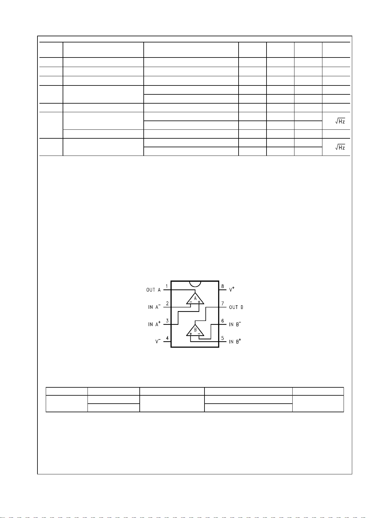
Connection Diagram
8-Pin SOIC
30015003
Top View
Ordering Information
Package Part Number Package Marking Transport Media NSC Drawing
8-Pin SOIC
LMP7732MA
LMP7732MA
95 units/Rails
M08A
LMP7732MAX 2.5k Units Tape and Reel
www.national.com 6
LMP7732

Typical Performance Characteristics Unless otherwise noted: T
A
= 25°C, RL > 10 kΩ, VCM = VS/2.
Offset Voltage Distribution
30015071
TCVOS Distribution
30015076
Offset Voltage Distribution
30015073
TCVOS Distribution
30015074
Offset Voltage Distribution
30015070
TCVOS Distribution
30015077
7 www.national.com
LMP7732

Offset Voltage Distribution
30015072
TCVOS Distribution
30015075
Offset Voltage vs. Temperature
30015082
Offset Voltage vs. Temperature
30015083
PSRR vs. Frequency
30015029
CMRR vs. Frequency
30015062
www.national.com 8
LMP7732

Offset Voltage vs. Supply Voltage
30015053
Offset Voltage vs. V
CM
30015054
Offset Voltage vs. V
CM
30015055
Offset Voltage vs. V
CM
30015056
Input Offset Voltage Time Drift
30015080
Slew Rate vs. Supply Voltage
30015020
9 www.national.com
LMP7732

Input Voltage Noise vs. Frequency
30015063
Input Current Noise vs. Frequency
30015064
Time Domain Voltage Noise
30015067
Time Domain Voltage Noise
30015065
Time Domain Voltage Noise
30015066
Output Voltage vs. Output Current
30015057
www.national.com 10
LMP7732

Input Bias Current vs. V
CM
30015025
Input Bias Current vs. V
CM
30015026
Input Bias Current vs. V
CM
30015027
Open Loop Frequency Response Over Temperature
30015018
Open Loop Frequency Response
30015019
Open Loop Frequency Response
30015028
11 www.national.com
LMP7732

THD+N vs. Frequency
30015085
THD+N vs. Output Voltage
30015069
Large Signal Step Response
30015022
Small Signal Step Response
30015021
Large Signal Step Response
30015024
Small Signal Step Response
30015023
www.national.com 12
LMP7732

Supply Current vs. Supply Voltage
30015081
Output Swing High vs. Supply Voltage
30015058
Output Swing Low vs. Supply Voltage
30015059
Sinking Current vs, Supply Voltage
30015060
Sourcing Current vs. Supply Voltage
30015061
13 www.national.com
LMP7732

Application Notes
LMP7732
The LMP7732 is a dual low noise, low offset voltage, rail-torail input and output, low voltage precision amplifier.
The low input voltage noise of only 2.9 nV/
with a 1/f corner at 3 Hz makes the LMP7732 ideal for sensor applications
where DC accuracy is of importance.
The LMP7732 has very low guaranteed offset voltage of only
±40 µV. This low offset voltage along with the very low input
voltage noise allows higher signal integrity and higher signal
to noise ratios since the error contribution by the amplifier is
at a minimum.
The LMP7732 has high gain bandwidth of 22 MHz. This wide
bandwidth enables the use of the amplifier at higher gain settings while retaining ample usable bandwidth for the application. This is particularly beneficial when system designers
need to use sensors with very limited output voltage range as
it allows larger gains in one stage which in turn increases signal to noise ratio.
The LMP7732 has a proprietary input bias cancellation circuitry on the input stages. This allows the LMP7732 to have
only about 1.5 nA bias current with a bipolar input stage. This
low input bias current, paired with the inherent lower input
voltage noise of bipolar input stages makes the LMP7732 an
excellent choice for precision applications. The combination
of low input bias current, low input offset voltage, and low input
voltage noise enables the user to achieve unprecedented accuracy and higher signal integrity.
National Semiconductor is heavily committed to precision
amplifiers and the market segment they serve. Technical support and extensive characterization data is available for sensitive applications or applications with a constrained error
budget.
The LMP7732 comes in the 8-pin SOIC package. This small
package is an ideal solution for area constrained PC boards
and portable electronics.
INPUT BIAS CURRENT CANCELLATION
The LMP7732 has proprietary input bias current cancellation
circuitry on its input stage.
The LMP7732 has rail-to-rail input. This is achieved by having
a p-input and n-input stage in parallel. Figure 1 only shows
one of the input stages as the circuitry is symmetrical for both
stages.
Figure 1 shows that as the common mode voltage gets closer
to one of the extreme ends, current I1 significantly increases.
This increased current shows as an increase in voltage drop
across resistor R1 equal to I1*R1 on IN+ of the amplifier. This
voltage contributes to the offset voltage of the amplifier. When
common mode voltage is in the mid-range, the transistors are
operating in the linear region and I1 is significantly small. The
voltage drop due to I1 across R1 can be ignored as it is orders
of magnitude smaller than the amplifier's input offset voltage.
As the common mode voltage gets closer to one of the rails,
the offset voltage generated due to I1 increases and becomes
comparable to the amplifiers offset voltage.
30015006
FIGURE 1. Input Bias Current Cancellation
INPUT VOLTAGE NOISE MEASUREMENT
The LMP7732 has very low input voltage noise. The peak-topeak input voltage noise of the LMP7732 can be measured
using the test circuit shown in Figure 2
30015079
FIGURE 2. 0.1 Hz to 10 Hz Noise Test Circuit
www.national.com 14
LMP7732

The frequency response of this noise test circuit at the 0.1 Hz
corner is defined by only one zero. The test time for the
0.1 Hz to 10 Hz noise measurement using this configuration
should not exceed 10 seconds, as this time limit acts as an
additional zero to reduce or eliminate the contributions of
noise from frequencies below 0.1 Hz.
Figure 3 shows typical peak-to-peak noise for the LMP7732
measured with the circuit in Figure 2.
30015066
FIGURE 3. 0.1 Hz to 10 Hz Input Voltage Noise
Measuring the very low peak-to-peak noise performance of
the LMP7732, requires special testing attention. In order to
achieve accurate results, the device should be warmed up for
at least five minutes. This is so that the input offset voltage of
the op amp settles to a value. During this warm up period, the
offset can typically change by a few µV because the chip
temperature increases by about 30°C. If the 10 seconds of
the measurement is selected to include this warm up time,
some of this temperature change might show up as the measured noise.Figure 4 shows the start-up drift of five typical
LMP7732 units.
30015080
FIGURE 4. Start-Up Input Offset Voltage Drift
During the peak-to-peak noise measurement, the LMP7732
must be shielded. This prevents offset variations due to airflow. Offset can vary by a few nV due to this airflow and that
can invalidate measurements of input voltage noise with a
magnitude which is in the same range. For similar reasons,
sudden motions must also be restricted in the vicinity of the
test area. The feed-through which results from this motion
could increase the observed noise value which in turn would
invalidate the measurement.
DIODES BETWEEN THE INPUTS
The LMP7732 has a set of anti-parallel diodes between their
input pins, as shown in Figure 5. These diodes are present to
protect the input stage of the amplifiers. At the same time,
they limit the amount of differential input voltage that is allowed on the input pins. A differential signal larger than the
voltage needed to turn on the diodes might cause damage to
the diodes. The differential voltage between the input pins
should be limited to ±3 diode drops or the input current needs
to be limited to ±20 mA.
30015004
FIGURE 5. Anti-Parallel Diodes between Inputs
15 www.national.com
LMP7732

DRIVING AN ADC
Analog to Digital Converters, ADCs, usually have a sampling
capacitor on their input. When the ADC's input is directly connected to the output of the amplifier a charging current flows
from the amplifier to the ADC. This charging current causes
a momentary glitch that can take some time to settle. There
are different ways to minimize this effect. One way is to slow
down the sampling rate. This method gives the amplifier sufficient time to stabilize its output. Another way to minimize the
glitch, caused by the switch capacitor, is to have an external
capacitor connected to the input of the ADC. This capacitor is
chosen so that its value is much larger than the internal
switching capacitor and it will hence provide the charge needed to quickly and smoothly charge the ADC's sampling capacitor. Since this large capacitor will be loading the output of
the amplifier as well, an isolation resistor is needed between
the output of the amplifier and this capacitor. The isolation
resistor, R
ISO
, separates the additional load capacitance from
the output of the amplifier and will also form a low-pass filter
and can be designed to provide noise reduction as well as
anti-aliasing. The draw back of having R
ISO
is that it reduces
signal swing since there is some voltage drop across it.
Figure 6 (a) shows the ADC directly connected to the ampli-
fier. To minimize the glitch in this setting, a slower sample rate
needs to be used. Figure 6 (b) shows R
ISO
and an external
capacitor used to minimize the glitch.
30015005
FIGURE 6. Driving An ADC
THERMOPILE AMPLIFIER
Thermopile Sensors
Thermopiles are arrays of interconnected thermocouples
which can detect surface temperature of an object through
radiation rather than direct contact. The hot and cold junctions
of the thermocouples are thermally isolated. The hot junctions
are exposed to IR radiation emitted from the measurement
surface and the cold junctions are connected to a heat sink.
The incident IR changes the temperature of the hot junctions
of the thermopile and produces an output voltage proportional
to this change.
The hot junction of the thermopile is covered with a highly
emissive coating. The IR radiation incident to this highly emissive material changes the temperature of this coating. The
temperature change is converted to a voltage by the thermopile. Emissivity represents the radiation or absorption efficiency of a material relative to a black body. An ideal black
body has an emissivity of 1.0. Excluding shiny metals, most
objects have emissivities above 0.85. As a practical matter,
shiny metals are not good candidates for IR sensing because
of their low emissivity. The low emissivity means that the material is highly reflective. Reflective materials often “reflect”
the surrounding environment's temperature rather than their
own heat radiation. This makes them not suitable for thermopile applications.
The output voltage of a thermopile is related to temperature
and emissivity by the following formula:
Where:
V
OUT
: Output voltage of the thermopile
K : Proportionality constant
ε
OBJ
: Emissivity of object being measured
T
OBJ
: Temperature of object being measured
δ : Correction factor. This is needed since thermopile filters
do not allow all wavelengths to enter the sensor
εTP: Emissivity of the thermopile
TTP: Temperature of the thermopile
As mentioned above, the IR radiation generates a static volt-
age across the pyroelectric material. If the illumination is
constant, the signal level detection declines. This is why the
radiation needs to be periodically refreshed. This task is usually achieved by the means of a mechanical chopper in front
of the detector.
Thermopiles offer much faster response time compared to
other temperature measurement devices. Packaged thermistors and thermocouples have response times that can range
up to a few seconds, where as packaged thermopiles can
easily achieve response times in the order of tens of milliseconds. Thermopiles also provide superior thermal isolation
compared to their contact temperature measurement counterparts. Physical contact disturbs the systems temperature
and also creates temperature gradients.
Figure 7 shows a simplified schematic of a thermopile. The
cold junctions are connected to a heat sink, and the absorber
material covers the hot junction. The output voltage resulting
from temperature difference between the two junctions is
measured at the two ends of the array of thermocouples. As
is evident in Figure 7, increasing the number of thermocouples in a thermopile increases the output voltage range. This
also increases the active area of the thermopile sensor.
www.national.com 16
LMP7732

30015007
FIGURE 7. Thermopile
Thermopiles have very wide temperature ranges of -100°C to
1000°C
When choosing a thermopile for a certain application, one
must pay attention to several parameters. Some of these parameters are discussed below:
Thermopiles' sensitivity, or responsivity, is determined by the
ratio of output voltage to the absorbed input signal power and
is usually specified in V/W. Typical sensitivity of thermopiles
ranges from 10s of V/W to about 100 V/W. Generally, higher
values of sensitivity are desirable. Sensitivity is dependent on
the absorber's area and number of thermocouples used in the
sensor. Sensitivity is often represented by S where:
S = V
OUT/PIN
The sensitivity of a thermopile changes with change in temperature. This change is usually specified as the Temperature
Coefficient, TC, of sensitivity. Lower numbers are desired for
this parameter.
Resistance of the thermopile is usually specified in the
datasheet. This is the impedance which will be seen by the
input of the amplifier used to process the thermopile's output
signal. Typical values for thermopile resistance, RTP, range
from 10s of kilo-ohms to about 100 kΩ. This resistance is also
a function of temperature. The temperature coefficient of the
resistance is usually specified in a thermopile's datasheet. As
with any other parameter, minimum variation with temperature is desired.
The dominant noise source for a thermopile is its resistance.
Noise spectral density of a resistor is calculated by:
Where k is the Boltzman constant and T is absolute temperature. Unit of noise spectral density is: V/
For the thermopile sensor, this noise is usually represented
by V
NOISE
where:
Typical values for this voltage noise are in the order of a few
tens of nV/ .
The Noise Equivalent Power, NEP, is often used to specify
the minimum detectable signal level per square root band-
width. A smaller NEP is desired, however NEP is dependent
on the thermopile active area, AD. For a thermopile:
And
As it is shown above, one cannot just compare the NEP of
two thermopiles without considering the corresponding active
areas.
A better way to compare thermopiles is to look at their specific
detectivity, D*. Specific detectivity includes both the device
noise and its sensitivity. It is normalized with respect to the
detector's active area and also noise bandwidth. D* is given
by:
Unit of D* is cm / W. Typical values for specific detectivity
range from 108 to 3*108 cm / W.
After receiving radiation, the thermopile takes some time before it comes to thermal equilibrium. The time it takes for the
sensor to achieve this equilibrium is called response time or
time constant of the sensor. Clearly, lower time constants are
very desirable.
Precision Amplifier
Since the output of thermopiles are usually very small and at
most in the order of only a few millivolts, the first part of the
signal conditioning path should involve amplification. In
choosing an amplifier for this purpose, a few different sensor
characteristics and the way they interface with the amplifier
should be considered. These are:
Sensor's Impedance and Opamp's Input Bias Current
The input bias current causes a voltage drop across the sen-
sor and the amount of this voltage is equal to the sensor's
impedance multiplied by the magnitude of bias current. The
higher the sensor's input impedance, the more accentuated
the effect of amplifier's input bias current will be. For very high
impedance sensors, it is imperative that opamps with very low
input bias currents be used. Thermopiles have input
impedances in the range of 100 kΩ, so input bias current is
not as critical as in some other applications.
Sensor's output voltage range:
The output signal of the sensor is fed into the opamp where
it will be amplified or otherwise conditioned, (e.g. level shifted,
buffered.) It is important to pay attention to different parameters of this output signal.
One important aspect is the lowest expected level of the
sensor's output and compare that with different parameters
contributing to the amplifier's total input noise. If the sensor's
output level is in the same order of magnitude or smaller than
the opamp's total input noise, then signal integrity at the
opamp's output and the ADC's input will be compromised.
17 www.national.com
LMP7732

30015078
FIGURE 8. Thermopile Amplifier
Figure 8 shows the LMP7732 used as a thermopile amplifier.
The LMP7732 is a great choice for use with thermopile sensors. The LMP7732 provides unprecedented accuracy and
precision because of its very low input voltage noise and the
very low 1/f corner frequency. The 1/f noise is one of the main
sources of error in DC operating mode. Since thermopiles and
most other sensors operate on DC signals, signal integrity at
the DC level is very important. The LMP7732 also has very
low offset voltage and offset voltage drift which greatly reduces the effects of input offset voltage of the amplifier on the
thermopile signal. The thermopile used in this circuit is
TPS332 from PerkinElmer Optoelectronics, PKI. This thermopile has an internal resistance, RTP, of 75 kΩ. The output
voltage of the thermopile is represented with a DC voltage
source. The TPS332 has a thermistor integrated in the package. The thermistor is used to measure the ambient temperature of the thermopile at the time of measurement. The
thermistor's resistance at room temperature is 30 kΩ. More
information about this thermopile and other sensors from PKI
can be found on http://www.perkinelmer.com/
The circuit in Figure 8 shows how the LMP7732 is connected
to the thermopile. This circuit is comprised of two LMP7732
amplifiers, the LM4140A-2.5 which is a precision voltage reference, the ADC122S021 which is a two channel Analog to
Digital converter, and the thermopile sensor. Note that the two
amplifiers used in this circuit are numbered for ease of refer-
ence. The LMP7732 amplifiers are referred to as amplifier 1
and amplifier 2 per Figure 8.
In Figure 8the LM4140A is providing a precision voltage reference of 2.5V. This reference voltage is applied to the thermistor via the 30 kΩ resistor. The thermistor's resistance is
converted to a voltage using this set up. This voltage is fed
into the ADC's channel one. The ADC uses this voltage and
the thermistor's look up table to convert this voltage to temperature. The 2.5V reference is also fed into amplifier 1, which
is configured as a buffer. This LMP7732 transfers the 2.5V
signal to both inputs of amplifier 2. This means the 2.5V will
show up on the output of amplifier 2. Having an output level
that is mid-supply is important since the thermopile sensor
has a bipolar output signal and this way the amplifier can accurately gain the thermopile voltage, whether its polarity is
positive or negative. It is also important because the output
signal of amplifier 2 is only positive. ADCs can only handle
positive signals on their inputs. Amplifier 2 is used to gain and
filter the thermopile signal. The low pass filter ensures that AC
noise will not be gained up and, as a result, the output signal
will be cleaner. The output of amplifier 2 is fed into the ADC's
channel 0. The ADC uses the ambient temperature, which
was calculated using the voltage on Channel 1 and the
thermistor's look up table, along with the thermopiles' gained
output voltage available on channel 0 and the thermopile's
look up table to determine the object's temperature.
www.national.com 18
LMP7732

Physical Dimensions inches (millimeters) unless otherwise noted
8-Pin SOIC
NS Package Number M08A
19 www.national.com
LMP7732

Notes
LMP7732 Low Noise, Precision, RRIO Amplifier
THE CONTENTS OF THIS DOCUMENT ARE PROVIDED IN CONNECTION WITH NATIONAL SEMICONDUCTOR CORPORATION
(“NATIONAL”) PRODUCTS. NATIONAL MAKES NO REPRESENTATIONS OR WARRANTIES WITH RESPECT TO THE ACCURACY
OR COMPLETENESS OF THE CONTENTS OF THIS PUBLICATION AND RESERVES THE RIGHT TO MAKE CHANGES TO
SPECIFICATIONS AND PRODUCT DESCRIPTIONS AT ANY TIME WITHOUT NOTICE. NO LICENSE, WHETHER EXPRESS,
IMPLIED, ARISING BY ESTOPPEL OR OTHERWISE, TO ANY INTELLECTUAL PROPERTY RIGHTS IS GRANTED BY THIS
DOCUMENT.
TESTING AND OTHER QUALITY CONTROLS ARE USED TO THE EXTENT NATIONAL DEEMS NECESSARY TO SUPPORT
NATIONAL’S PRODUCT WARRANTY. EXCEPT WHERE MANDATED BY GOVERNMENT REQUIREMENTS, TESTING OF ALL
PARAMETERS OF EACH PRODUCT IS NOT NECESSARILY PERFORMED. NATIONAL ASSUMES NO LIABILITY FOR
APPLICATIONS ASSISTANCE OR BUYER PRODUCT DESIGN. BUYERS ARE RESPONSIBLE FOR THEIR PRODUCTS AND
APPLICATIONS USING NATIONAL COMPONENTS. PRIOR TO USING OR DISTRIBUTING ANY PRODUCTS THAT INCLUDE
NATIONAL COMPONENTS, BUYERS SHOULD PROVIDE ADEQUATE DESIGN, TESTING AND OPERATING SAFEGUARDS.
EXCEPT AS PROVIDED IN NATIONAL’S TERMS AND CONDITIONS OF SALE FOR SUCH PRODUCTS, NATIONAL ASSUMES NO
LIABILITY WHATSOEVER, AND NATIONAL DISCLAIMS ANY EXPRESS OR IMPLIED WARRANTY RELATING TO THE SALE
AND/OR USE OF NATIONAL PRODUCTS INCLUDING LIABILITY OR WARRANTIES RELATING TO FITNESS FOR A PARTICULAR
PURPOSE, MERCHANTABILITY, OR INFRINGEMENT OF ANY PATENT, COPYRIGHT OR OTHER INTELLECTUAL PROPERTY
RIGHT.
LIFE SUPPORT POLICY
NATIONAL’S PRODUCTS ARE NOT AUTHORIZED FOR USE AS CRITICAL COMPONENTS IN LIFE SUPPORT DEVICES OR
SYSTEMS WITHOUT THE EXPRESS PRIOR WRITTEN APPROVAL OF THE CHIEF EXECUTIVE OFFICER AND GENERAL
COUNSEL OF NATIONAL SEMICONDUCTOR CORPORATION. As used herein:
Life support devices or systems are devices which (a) are intended for surgical implant into the body, or (b) support or sustain life and
whose failure to perform when properly used in accordance with instructions for use provided in the labeling can be reasonably expected
to result in a significant injury to the user. A critical component is any component in a life support device or system whose failure to perform
can be reasonably expected to cause the failure of the life support device or system or to affect its safety or effectiveness.
National Semiconductor and the National Semiconductor logo are registered trademarks of National Semiconductor Corporation. All other
brand or product names may be trademarks or registered trademarks of their respective holders.
Copyright© 2007 National Semiconductor Corporation
For the most current product information visit us at www.national.com
National Semiconductor
Americas Customer
Support Center
Email:
new.feedback@nsc.com
Tel: 1-800-272-9959
National Semiconductor Europe
Customer Support Center
Fax: +49 (0) 180-530-85-86
Email: europe.support@nsc.com
Deutsch Tel: +49 (0) 69 9508 6208
English Tel: +49 (0) 870 24 0 2171
Français Tel: +33 (0) 1 41 91 8790
National Semiconductor Asia
Pacific Customer Support Center
Email: ap.support@nsc.com
National Semiconductor Japan
Customer Support Center
Fax: 81-3-5639-7507
Email: jpn.feedback@nsc.com
Tel: 81-3-5639-7560
www.national.com
 Loading...