

LMP7707/LMP7708/LMP7709
Precision, CMOS Input, RRIO, Wide Supply Range
Decompensated Amplifiers
July 30, 2008
LMP7707/LMP7708/LMP7709 Precision, CMOS Input, RRIO, Wide Supply Range Decompensated
Amplifiers
General Description
The LMP7707/LMP7708/LMP7709 devices are single, dual,
and quad low offset voltage, rail-to-rail input and output precision amplifiers which each have a CMOS input stage and a
wide supply voltage range. The LMP7707/LMP7708/
LMP7709 are part of the LMP® precision amplifier family and
are ideal for sensor interface and other instrumentation applications. These decompensated amplifiers are stable at a
gain of 6 and higher.
The guaranteed low offset voltage of less than ±200 µV along
with the guaranteed low input bias current of less than ±1 pA
make the LMP7707/LMP7708/LMP7709 ideal for precision
applications. The LMP7707/LMP7708/LMP7709 are built utilizing VIP50 technology, which allows the combination of a
CMOS input stage and a supply voltage range of 12V with
rail-to-rail common mode voltage capability. The LMP7707/
LMP7708/LMP7709 are the perfect choice in many applications where conventional CMOS parts cannot operate due to
the voltage conditions.
The unique design of the rail-to-rail input stage of each of the
LMP7707/LMP7708/LMP7709 significantly reduces the CMRR glitch commonly associated with rail-to-rail input amplifiers. Both sides of the complimentary input stage have been
trimmed, thereby reducing the difference between the NMOS
and PMOS offsets. The output swings within 40 mV of either
rail to maximize the signal dynamic range in applications requiring low supply voltage.
The LMP7707 is offered in the space saving 5-Pin SOT23 and
8-pin SOIC package, the LMP7708 is offered in the 8-Pin
MSOP and 8-pin SOIC package and the quad LMP7709 is
offered in the 14-Pin TSSOP and the 14-pin SOIC package.
These small packages are ideal solutions for area constrained PC boards and portable electronics.
Features
Unless otherwise noted, typical values at VS = 5V.
Input offset voltage (LMP7707) ±200 µV (max)
■
Input offset voltage (LMP7708/LMP7709) ±220 µV (max)
■
Input bias current ±200 fA
■
Input voltage noise 9 nV/√Hz
■
CMRR 130 dB
■
Open loop gain 130 dB
■
Temperature range −40°C to 125°C
■
Gain bandwidth product (AV =10) 14 MHz
■
Stable at a gain of 10 or higher
■
Supply current (LMP7707) 715 µA
■
Supply current (LMP7708) 1.5 mA
■
Supply current (LMP7709) 2.9 mA
■
Supply voltage range 2.7V to 12V
■
Rail-to-rail input and output
■
Applications
High impedance sensor interface
■
Battery powered instrumentation
■
High gain amplifiers
■
DAC buffer
■
Instrumentation amplifier
■
Active filters
■
Open Loop Frequency Response
Increased Bandwidth for Same Supply Current at AV> 10
LMP® is a registered trademark of National Semiconductor Corporation.
© 2008 National Semiconductor Corporation 202037 www.national.com
20203764
Absolute Maximum Ratings (Note 1)
If Military/Aerospace specified devices are required,
please contact the National Semiconductor Sales Office/
Distributors for availability and specifications.
ESD Tolerance (Note 2)
Human Body Model 2000V
Machine Model 200V
Charge Device Model 1000V
V
Differential
IN
Supply Voltage (VS = V+ – V−)
LMP7707/LMP7708/LMP7709
Voltage at Input/Output Pins V++ 0.3V to V− − 0.3V
Input Current 10 mA
Storage Temperature Range −65°C to +150°C
Junction Temperature (Note 3) +150°C
±300 mV
13.2V
Soldering Information
Infrared or Convection (20 sec) 235°C
Wave Soldering Lead Temp. (10
sec) 260°C
Operating Ratings (Note 1)
Temperature Range (Note 3) −40°C to +125°C
Supply Voltage (VS = V+ – V−)
Package Thermal Resistance (θJA) (Note 3)
5-Pin SOT23 265°C/W
8-Pin SOIC 190°C/W
8-Pin MSOP 235°C/W
14-Pin TSSOP 122°C/W
14-Pin SOIC 145°C/W
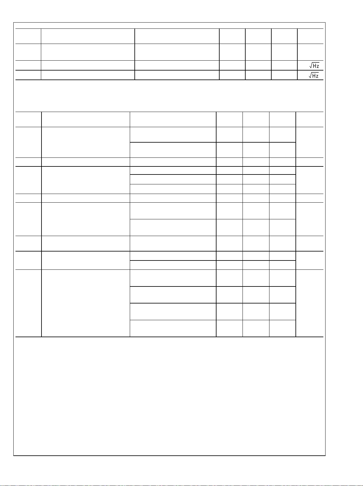
3V Electrical Characteristics (Note 4)
Unless otherwise specified, all limits are guaranteed for TA = 25°C, V+ = 3V, V− = 0V, VCM = V+/2, and RL > 10 kΩ to V+/2.
Boldface limits apply at the temperature extremes.
Symbol Parameter Conditions Min
(Note 6)
V
OS
TCV
I
B
I
OS
CMRR Common Mode Rejection Ratio
PSRR Power Supply Rejection Ratio
CMVR Input Common-Mode Voltage Range
A
VOL
Input Offset Voltage LMP7707 ±37 ±200
LMP7708/LMP7709 ±56 ±220
Input Offset Voltage Drift (Note 7) ±1 ±5
OS
Input Bias Current (Notes 7, 8) ±0.2 ±1
−40°C ≤ TA ≤ 85°C
−40°C ≤ TA ≤ 125°C
Input Offset Current 40 fA
Open Loop Voltage Gain
0V ≤ V
LMP7707
0V ≤ V
LMP7708/LMP7709
2.7V ≤ V+ ≤ 12V, VO = V+/2
CMRR ≥ 80 dB
CMRR ≥ 77 dB
RL = 2 kΩ (LMP7707)
VO = 0.3V to 2.7V
RL = 2 kΩ (LMP7708/LMP7709)
VO = 0.3V to 2.7V
RL = 10 kΩ
VO = 0.2V to 2.8V
CM
CM
≤ 3V
≤ 3V
±400
−0.2 3.2
−0.2 3.2
100
100
100
±50
86
80
84
78
86
82
96
94
96
Typ
(Note 5)
130
130
98
114
114
124
Max
(Note 6)
±500
±520
2.7V to 12V
Units
μV
μV/°C
pA
dB
dB
V
dB
www.national.com 2
LMP7707/LMP7708/LMP7709
Symbol Parameter Conditions Min
(Note 6)
V
O
Output Swing High
RL = 2 kΩ to V+/2
LMP7707
RL = 2 kΩ to V+/2
LMP7708/LMP7709
RL = 10 kΩ to V+/2
LMP7707
RL = 10 kΩ to V+/2
LMP7708/LMP7709
Output Swing Low
RL = 2 kΩ to V+/2
LMP7707
RL = 2 kΩ to V+/2
LMP7708/LMP7709
RL = 10 kΩ to V+/2
LMP7707
RL = 10 kΩ to V+/2
LMP7708/LMP7709
I
O
Output Short Circuit Current
(Notes 3, 9)
Sourcing VO = V+/2
VIN = 100 mV
Sinking VO = V+/2
VIN = −100 mV (LMP7707)
Sinking VO = V+/2
VIN = −100 mV (LMP7708/
40 80
40 80
30 40
35 50
40 60
45 100
20 40
20 50
25
15
25
20
25
15
Typ
(Note 5)
42
42
42
Max
(Note 6)
120
150
60
100
80
170
50
90
Units
mV
from V
mV
mA
LMP7709)
I
S
Supply Current LMP7707 0.670 1.0
1.2
LMP7708 1.4 1.8
2.1
mA
LMP7709 2.9 3.5
4.5
SR Slew Rate (Note 10) VO = 2 V
10% to 90% 5.1
PP,
V/μs
GBWP Gain Bandwidth Product AV = 10 13 MHz
THD+N Total Harmonic Distortion + Noise f = 1 kHz, AV = 10, VO = 2.5V,
0.024 %
RL = 10 kΩ
e
n
i
n
Input-Referred Voltage Noise f = 1 kHz 9
Input-Referred Current Noise f = 100 kHz 1
nV/
fA/
+
5V Electrical Characteristics (Note 4)
Unless otherwise specified, all limits are guaranteed for TA = 25°C, V+ = 5V, V− = 0V, VCM = V+/2, and RL > 10 kΩ to V+/2.
Boldface limits apply at the temperature extremes.
Symbol Parameter Conditions Min
(Note 6)
V
OS
Input Offset Voltage LMP7707 ±37 ±200
LMP7708/LMP7709 ±32 ±220
TCV
I
B
Input Offset Voltage Drift (Note 7) ±1 ±5
OS
Input Bias Current (Notes 7, 8) ±0.2 ±1
−40°C ≤ TA ≤ 85°C
−40°C ≤ TA ≤ 125°C
3 www.national.com
±400
±50
Typ
(Note 5)
Max
(Note 6)
±500
±520
Units
μV
μV/°C
pA
Symbol Parameter Conditions Min
(Note 6)
I
OS
CMRR Common Mode Rejection Ratio
Input Offset Current 40
0V ≤ V
CM
≤ 5V
LMP7707
0V ≤ V
CM
≤ 5V
LMP7708/LMP7709
PSRR Power Supply Rejection Ratio
2.7V ≤ V+ ≤ 12V, VO = V+/2
88
83
86
81
86
Typ
(Note 5)
130
130
100
Max
(Note 6)
82
CMVR Input Common-Mode Voltage Range
LMP7707/LMP7708/LMP7709
A
VOL
V
O
I
O
Open Loop Voltage Gain
Output Swing High
Output Swing Low
Output Short Circuit Current
(Notes 3, 9)
CMRR ≥ 80 dB
CMRR ≥ 78 dB
RL = 2 kΩ (LMP7707)
VO = 0.3V to 4.7V
RL = 2 kΩ (LMP7708/LMP7709)
VO = 0.3V to 4.7V
RL = 10 kΩ
VO = 0.2V to 4.8V
RL = 2 kΩ to V+/2
LMP7707
RL = 2 kΩ to V+/2
LMP7708/LMP7709
RL = 10 kΩ to V+/2
LMP7707
RL = 10 kΩ to V+/2
LMP7708/LMP7709
RL = 2 kΩ to V+/2
LMP7707
RL = 2 kΩ to V+/2
LMP7708/LMP7709
RL = 10 kΩ to V+/2
LMP7707
RL = 10 kΩ to V+/2
LMP7708/LMP7709
Sourcing VO = V+/2
VIN = 100 mV (LMP7707)
Sourcing VO = V+/2
VIN = 100 mV (LMP7708/LMP7709)
Sinking VO = V+/2
VIN = −100 mV (LMP7707)
Sinking VO = V+/2
VIN = −100 mV (LMP7708/
−0.2 5.2
−0.2 5.2
100
119
96
100
119
94
100
130
96
60 110
130
60 120
200
40 50
70
40 60
120
50 80
90
50 120
190
30 40
50
30 50
100
40
66
28
38
66
25
40
76
28
40
76
23
LMP7709)
I
S
Supply Current LMP7707 0.715 1.0
1.2
LMP7708 1.5 1.9
2.2
LMP7709 2.9 3.7
4.6
SR Slew Rate (Note 10) VO = 4 VPP, 10% to 90% 5.6
GBWP Gain Bandwidth Product AV = 10 14 MHz
Units
fA
dB
dB
V
dB
mV
from V
mV
mA
mA
V/μs
+
www.national.com 4
LMP7707/LMP7708/LMP7709
Symbol Parameter Conditions Min
(Note 6)
THD+N Total Harmonic Distortion + Noise f = 1 kHz, AV = 10, VO = 4.5V,
0.024 %
Typ
(Note 5)
Max
(Note 6)
RL = 10 kΩ
e
n
i
n
Input-Referred Voltage Noise f = 1 kHz 9
Input-Referred Current Noise f = 100 kHz 1
±5V Electrical Characteristics (Note 4)
Unless otherwise specified, all limits are guaranteed for TA = 25°C, V+ = 5V, V− = −5V, VCM = 0V, and RL > 10 kΩ to 0V. Boldface limits apply at the temperature extremes.
Symbol Parameter Conditions Min
(Note 6)
V
OS
Input Offset Voltage LMP7707 ±37 ±200
LMP7708/LMP7709 ±37 ±220
TCV
I
B
Input Offset Voltage Drift (Note 7) ±1 ±5
OS
Input Bias Current (Notes 7, 8) ±0.2 1
−40°C ≤ TA ≤ 85°C
±400
I
OS
Input Offset Current 40
CMRR Common Mode Rejection Ratio
−40°C ≤ TA ≤ 125°C
−5V ≤ V
CM
≤ 5V
LMP7707
−5V ≤ V
CM
≤ 5V
LMP7708/LMP7709
PSRR Power Supply Rejection Ratio
CMVR Input Common-Mode Voltage Range
A
VOL
Open Loop Voltage Gain
2.7V ≤ V+ ≤ 12V, V− = 0V, VO = V+/2
CMRR ≥ 80 dB
CMRR ≥ 78 dB
RL = 2 kΩ (LMP7707)
−5.2 5.2
−5.2 5.2
100
VO = −4.7V to 4.7V
RL = 2 kΩ (LMP7708/LMP7709)
100
VO = −4.7V to 4.7V
RL = 10 kΩ (LMP7707)
100
VO = −4.8V to 4.8V
RL = 10 kΩ (LMP7708/LMP7709)
100
VO = −4.8V to 4.8V
±50
92
88
90
86
86
82
98
94
98
97
Typ
(Note 5)
138
138
98
121
121
134
134
Max
(Note 6)
±500
±520
Units
nV/
fA/
Units
μV
μV/°C
pA
fA
dB
dB
V
dB
5 www.national.com
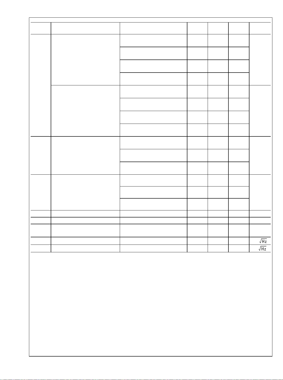
Symbol Parameter Conditions Min
V
O
Output Swing High
RL = 2 kΩ to 0V
LMP7707
RL = 2 kΩ to 0V
LMP7708/LMP7709
RL = 10 kΩ to 0V
LMP7707
RL = 10 kΩ to 0V
LMP7708/LMP7709
LMP7707/LMP7708/LMP7709
Output Swing Low
RL = 2 kΩ to 0V
LMP7707
RL = 2 kΩ to 0V
LMP7708/LMP7709
RL = 10 kΩ to 0V
LMP7707
RL = 10 kΩ to 0V
LMP7708/LMP7709
I
O
Output Short Circuit Current
(Notes 3, 9)
Sourcing VO = 0V
VIN = 100 mV (LMP7707)
Sourcing VO = 0V
VIN = 100 mV (LMP7708/LMP7709)
Sinking VO = 0V
VIN = −100 mV
I
S
Supply Current LMP7707 0.790 1.1
(Note 6)
90 150
90 180
40 80
40 80
90 130
90 180
40 50
40 60
50
35
48
33
50
35
Typ
(Note 5)
86
86
84
Max
(Note 6)
170
290
100
150
150
290
60
110
1.3
LMP7708 1.7 2.1
2.5
LMP7709 3.2 4.2
5.0
SR Slew Rate (Note 10) VO = 9 VPP, 10% to 90% 5.9
GBWP Gain Bandwidth Product AV = 10 15 MHz
THD+N Total Harmonic Distortion + Noise f = 1 kHz, AV = 10, VO = 9V,
0.024 %
RL = 10 kΩ
e
n
i
n
Input-Referred Voltage Noise f = 1 kHz 9
Input-Referred Current Noise f = 100 kHz 1
Units
mV
from V
mV
from V
mA
mA
V/μs
nV/
fA/
+
–
Note 1: Absolute Maximum Ratings indicate limits beyond which damage to the device may occur. Operating Ratings indicate conditions for which the device is
intended to be functional, but specific performance is not guaranteed. For guaranteed specifications and the test conditions, see the Electrical Characteristics
Tables.
Note 2: Human Body Model, applicable std. MIL-STD-883, Method 3015.7. Machine Model, applicable std. JESD22-A115-A (ESD MM std. of JEDEC)
Field-Induced Charge-Device Model, applicable std. JESD22-C101-C (ESD FICDM std. of JEDEC).
Note 3: The maximum power dissipation is a function of T
PD = (T
Note 4: Electrical table values apply only for factory testing conditions at the temperature indicated. Factory testing conditions result in very limited self-heating
of the device.
Note 5: Typical values represent the most likely parametric norm as determined at the time of characterization. Actual typical values may vary over time and will
also depend on the application and configuration. The typical values are not tested and are not guaranteed on shipped production material.
Note 6: Limits are 100% production tested at 25°C. Limits over the operating temperature range are guaranteed through correlations using the Statistical Quality
Control (SQC) method.
Note 7: This parameter is guaranteed by design and/or characterization and is not tested in production.
Note 8: Positive current corresponds to current flowing into the device.
Note 9: The short circuit test is a momentary test.
Note 10: The number specified is the slower of positive and negative slew rates.
www.national.com 6
- TA)/ θJA . All numbers apply for packages soldered directly onto a PC board.
J(MAX)
, θJA. The maximum allowable power dissipation at any ambient temperature is
J(MAX)
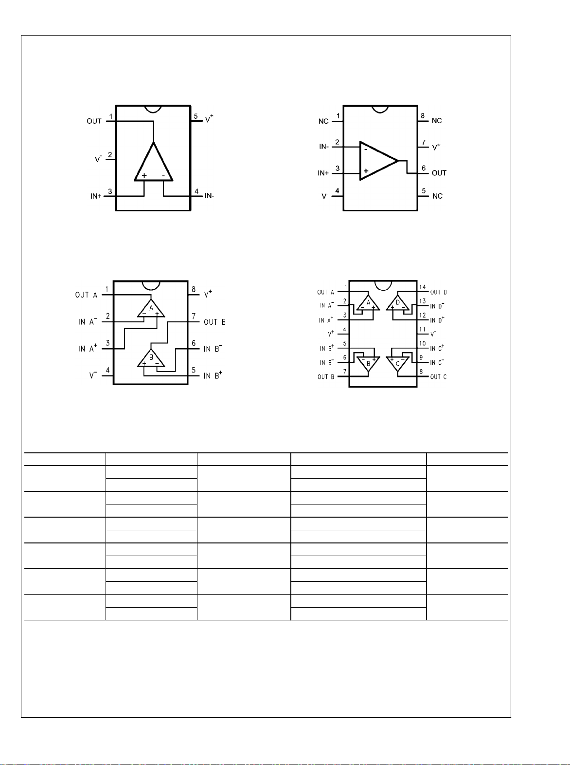
Connection Diagrams
LMP7707/LMP7708/LMP7709
LMP7707
5-Pin SOT23
Top View
LMP7708
8-Pin MSOP/SOIC
20203702
LMP7707
8-Pin SOIC
Top View
LMP7709
14-Pin TSSOP/SOIC
20203701
Top View
20203703
Top View
20203704
Ordering Information
Package Part Number Package Marking Transport Media NSC Drawing
5-Pin SOT23
8-Pin SOIC
8-Pin MSOP
8-Pin SOIC
14-Pin TSSOP
14-Pin SOIC
LMP7707MF
LMP7707MFX 3k Units Tape and Reel
LMP7707MA
LMP7707MAX 2.5k Units Tape and Reel
LMP7708MM
LMP7708MMX 3.5k Units Tape and Reel
LMP7708MA
LMP7708MAX 2.5k Units Tape and Reel
LMP7709MT
LMP7709MTX 2.5k Units Tape and Reel
LMP7709MA
LMP7709MAX 2.5 Units Tape and Reel
AH4A
LMP7707MA
AJ4A
LMP7708MA
LMP7709MT
LMP7709MA
1k Units Tape and Reel
95 Units/Rail
1k Units Tape and Reel
95 Units/Rail
94 Units/Rail
55 Units/Rail
MF05A
M08A
MUA08A
M08A
MTC14
M14A
7 www.national.com
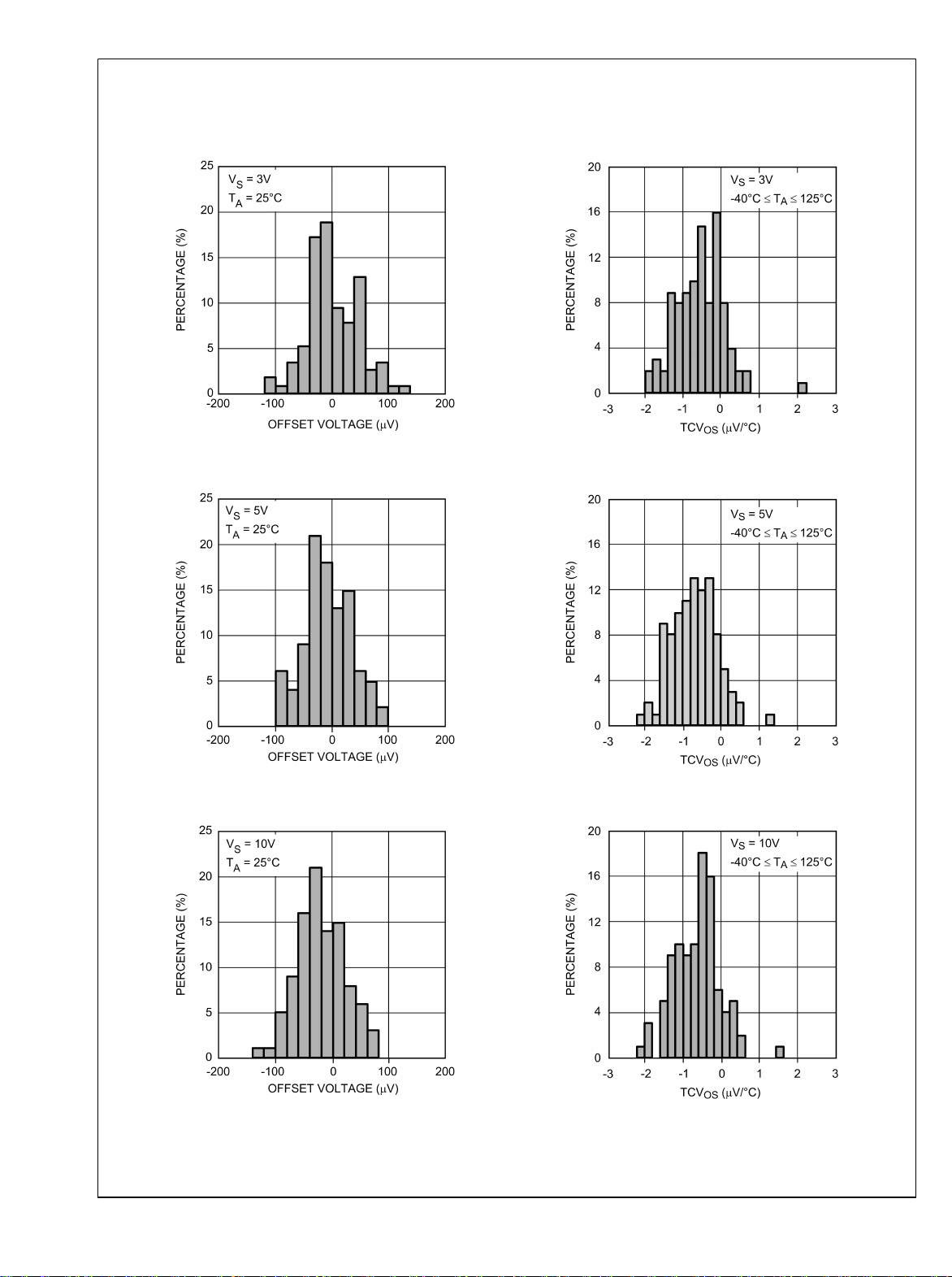
Typical Performance Characteristics Unless otherwise specified, T
connected to (V++V−)/2
= 25°C, VCM = VS/2, RL > 10 kΩ
A
Offset Voltage Distribution
LMP7707/LMP7708/LMP7709
Offset Voltage Distribution
20203736
TCVOS Distribution
20203741
TCVOS Distribution
20203737
Offset Voltage Distribution
20203738
www.national.com 8
20203742
TCVOS Distribution
20203743

LMP7707/LMP7708/LMP7709
Offset Voltage vs. Temperature
Offset Voltage vs. Supply Voltage
20203706
CMRR vs. Frequency
Offset Voltage vs. V
20203750
CM
Offset Voltage vs. V
CM
20203710
20203708
Offset Voltage vs. V
20203707
CM
20203709
9 www.national.com

Input Bias Current vs. V
LMP7707/LMP7708/LMP7709
CM
Input Bias Current vs. V
CM
Input Bias Current vs. V
Input Bias Current vs. V
CM
CM
20203746
20203747
Input Bias Current vs. V
Input Bias Current vs. V
20203730
CM
20203731
CM
20203748
www.national.com 10
20203749

LMP7707/LMP7708/LMP7709
PSRR vs. Frequency
Sinking Current vs. Supply Voltage
20203745
Supply Current vs. Supply Voltage (Per Channel)
20203711
Sourcing Current vs. Supply Voltage
Output Voltage vs. Output Current
20203713
20203716
20203712
Slew Rate vs. Supply Voltage
20203717
11 www.national.com

Open Loop Frequency Response
LMP7707/LMP7708/LMP7709
Open Loop Frequency Response
Small Signal Step Response, AV = 10
20203719
Small Signal Step Response, AV = 100
20203715
20203714
Large Signal Step Response, AV = 10
20203718
Large Signal Step Response, AV = 100
20203726
www.national.com 12
20203720

LMP7707/LMP7708/LMP7709
Input Voltage Noise vs. Frequency
Output Swing High vs. Supply Voltage
20203727
Open Loop Gain vs. Output Voltage Swing
20203752
Output Swing Low vs. Supply Voltage
20203733
Output Swing High vs. Supply Voltage
20203732
20203735
Output Swing Low vs. Supply Voltage
20203734
13 www.national.com

THD+N vs. Frequency
LMP7707/LMP7708/LMP7709
THD+N vs. Output Voltage
20203728
Crosstalk Rejection Ratio vs. Frequency
(LMP7708/LMP7709)
20203753
20203729
www.national.com 14

Application Information
LMP7707/LMP7708/LMP7709
The LMP7707/LMP7708/LMP7709 devices are single, dual
and quad low offset voltage, rail-to-rail input and output precision amplifiers each with a CMOS input stage and the wide
supply voltage range of 2.7V to 12V. The LMP7707/
LMP7708/LMP7709 have a very low input bias current of only
±200 fA at room temperature.
The wide supply voltage range of 2.7V to 12V over the extensive temperature range of −40°C to 125°C makes either
the LMP7707, LMP7708 or LMP7709 an excellent choice for
low voltage precision applications with extensive temperature
requirements.
The LMP7707/LMP7708/LMP7709 have only ±37 µV of typical input referred offset voltage and this offset is guaranteed
to be less than ±500 µV for the single and ±520 µV for the
dual and quad over temperature. This minimal offset voltage
allows more accurate signal detection and amplification in
precision applications.
The low input bias current of only ±200 fA along with the low
input referred voltage noise of 9 nV/
LMP7708/LMP7709 superior qualities for use in sensor applications. Lower levels of noise introduced by the amplifier
mean better signal fidelity and a higher signal-to-noise ratio.
The LMP7707/LMP7708/LMP7709 are stable for a gain of 6
or higher. With proper compensation though, the LMP7707,
LMP7708 or LMP7709 can be operational at a gain of ±1 and
still maintain much faster slew rates than comparable fully
compensated amplifiers. The increase in bandwidth and slew
rate is obtained without any additional power consumption.
National Semiconductor is heavily committed to precision
amplifiers and the market segment they serve. Technical support and extensive characterization data is available for sensitive applications or applications with a constrained error
budget.
The LMP7707 is offered in the space saving 5-Pin SOT23 and
8-Pin SOIC package, the LMP7708 comes in the 8-pin MSOP
and 8-Pin SOIC package and the LMP7709 is offered in the
14-Pin TSSOP and 14-Pin SOIC package. These small packages are ideal solutions for area constrained PC boards and
portable electronics.
give the LMP7707/
20203721
FIGURE 1. Isolating Capacitive Load
INPUT CAPACITANCE
CMOS input stages inherently have low input bias current and
higher input referred voltage noise. The LMP7707/LMP7708/
LMP7709 enhances this performance by having the low input
bias current of only ±200 fA, as well as a very low input referred voltage noise of 9 nV/
. In order to achieve this a
large input stage has been used. This large input stage increases the input capacitance of the LMP7707/LMP7708/
LMP7709. The typical value of this input capacitance, CIN, for
the LMP7707/LMP7708/LMP7709 is 25 pF. The input capacitance will interact with other impedances such as gain and
feedback resistors, which are seen on the inputs of the amplifier, to form a pole. This pole will have little or no effect on
the output of the amplifier at low frequencies and DC conditions, but will play a bigger role as the frequency increases.
At higher frequencies, the presence of this pole will decrease
phase margin and will also cause gain peaking. In order to
compensate for the input capacitance, care must be taken in
choosing the feedback resistors. In addition to being selective
in picking values for the feedback resistor, a capacitor can be
added to the feedback path to increase stability.
LMP7707/LMP7708/LMP7709
CAPACITIVE LOAD
The LMP7707/LMP7708/LMP7709 devices can each be connected as a non-inverting voltage follower. This configuration
is the most sensitive to capacitive loading.
The combination of a capacitive load placed on the output of
an amplifier along with the amplifier’s output impedance creates a phase lag which in turn reduces the phase margin of
the amplifier. If the phase margin is significantly reduced, the
response will be either underdamped or it will oscillate.
In order to drive heavier capacitive loads, an isolation resistor,
R
, as shown in the circuit in Figure 1 should be used. By
ISO
using this isolation resistor, the capacitive load is isolated
from the amplifier’s output, and hence, the pole caused by
CL is no longer in the feedback loop. The larger the value of
R
, the more stable the output voltage will be. If values of
ISO
R
are sufficiently large, the feedback loop will be stable,
ISO
independent of the value of CL. However, larger values of
R
result in reduced output swing and reduced output cur-
ISO
rent drive.
20203744
FIGURE 2. Compensating for Input Capacitance
Using this compensation method will have an impact on the
high frequency gain of the op amp, due to the frequency dependent feedback of this amplifier. Low gain settings can,
again, introduce instability issues.
DIODES BETWEEN THE INPUTS
The LMP7707/LMP7708/LMP7709 have a set of anti-parallel
diodes between the input pins, as shown in Figure 3. These
diodes are present to protect the input stage of the amplifier.
At the same time, they limit the amount of differential input
voltage that is allowed on the input pins. A differential signal
larger than one diode voltage drop might damage the diodes.
The differential signal between the inputs needs to be limited
to ±300 mV or the input current needs to be limited to ±10 mA.
Exceeding these limits will damage the part.
15 www.national.com

LMP7707/LMP7708/LMP7709
FIGURE 3. Input of the LMP7707
TOTAL NOISE CONTRIBUTION
The LMP7707/LMP7708/LMP7709 have very low input bias
current, very low input current noise and very low input voltage noise. As a result, these amplifiers are ideal choices for
circuits with high impedance sensor applications.
Figure 4 shows the typical input noise of the LMP7707/
LMP7708/LMP7709 as a function of source resistance. The
total noise at the input can be calculated using Equation 1.
Where:
eni is the total noise on the input.
en denotes the input referred voltage noise
ei is the voltage drop across source resistance due to input
referred current noise or ei = RS * i
n
et is the thermal noise of the source resistance
The input current noise of the LMP7707/LMP7708/LMP7709
is so low that it will not become the dominant factor in the total
noise unless source resistance exceeds 300 MΩ, which is an
unrealistically high value.
As is evident in Figure 4, at lower RS values, the total noise
is dominated by the amplifier’s input voltage noise. Once R
is larger than a few kilo-Ohms, then the dominant noise factor
becomes the thermal noise of RS. As mentioned before, the
current noise will not be the dominant noise factor for any
practical application.
20203725
(1)
HIGH IMPEDANCE SENSOR INTERFACE
Many sensors have high source impedances that may range
up to 10 MΩ. The output signal of sensors often needs to be
amplified or otherwise conditioned by means of an amplifier.
The input bias current of this amplifier can load the sensor’s
output and cause a voltage drop across the source resistance
as shown in Figure 5, where VIN + = VS – I
The last term, I
prevent errors introduced to the system due to this voltage,
, shows the voltage drop across RS. To
BIAS*RS
BIAS*RS
an op amp with very low input bias current must be used with
high impedance sensors. This is to keep the error contribution
by I
so that it will not become the dominant noise factor. The
less than the input voltage noise of the amplifier,
BIAS*RS
LMP7707/LMP7708/LMP7709 have very low input bias current, typically 200 fA.
20203759
FIGURE 5. Noise Due to I
BIAS
USAGE OF DECOMPENSATED AMPLIFIERS
This section discusses the differences between compensated
and decompensated op amps and presents the advantages
S
of decompensated amplifiers. In high gain applications decompensated amplifiers can be used without any changes
compared to standard amplifiers. However, for low gain applications special frequency compensation measures have to
be taken to ensure stability.
Feedback circuit theory is discussed in detail, in particular as
it applies to decompensated amplifiers. Bode plots are presented for a graphical explanation of stability analysis. Two
solutions are given for creating a feedback network for decompensated amplifiers when relatively low gains are required: A simple resistive feedback network and a more
advanced frequency dependent feedback network with improved noise performance. Finally, a design example is presented resulting in a practical application. The results are
compared to fully compensated amplifiers (National Semiconductors LMP7701/LMP7702/LMP7704).
20203758
FIGURE 4. Total Input Noise
www.national.com 16
COMPENSATED AMPLIFIERS
A (fully) compensated op amp is designed to operate with
good stability down to gains of ±1. For this reason, the compensated op amp is also called a unity gain stable op amp.
Figure 6 shows the Open Loop Response of a compensated
amplifier.

LMP7707/LMP7708/LMP7709
202037aa
FIGURE 6. Open Loop Frequency Response
Compensated Amplifier (LMP7701)
This amplifier is unity gain stable, because the phase shift is
still < 180°, when the gain crosses 0 dB (unity gain).
Stability can be expressed in two different ways:
Phase Margin
This is the phase difference between the actual phase shift and 180°, at the point where
the gain is 0 dB.
Gain Margin
This is the gain difference relative to 0 dB, at
the frequency where the phase shift crosses
the 180°.
The amplifier is supposed to be used with negative feedback
but a phase shift of 180° will turn the negative feedback into
positive feedback, resulting in oscillations. A phase shift of
180° is not a problem when the gain is smaller than 0 dB, so
the critical point for stability is 180° phase shift at 0 dB gain.
The gain margin and phase margin express the margin enhancing overall stability between the amplifiers response and
this critical point.
DECOMPENSATED AMPLIFIERS
Decompensated amplifiers, such as the LMP7707/LMP7708/
LMP7709, are designed to maximize the bandwidth and slew
rate without any additional power consumption over the unity
gain stable op amp. That is, a decompensated op amp has a
higher bandwidth to power ratio than an equivalent compensated op amp. Compared with the unity gain stable amplifier,
the decompensated version has the following advantages:
1.
A wider closed loop bandwidth.
2.
Better slew rate due to reduced compensation
capacitance within the op amp.
3.
Better Full Power Bandwidth, given with Equation 2.
(2)
Figure 7 shows the frequency response of the decompensated amplifier.
202037a9
FIGURE 7. Open Loop Frequency Response
Decompensated Amplifier (LMP7707)
As shown in Figure 7, the reduced internal compensation
moves the first pole to higher frequencies. The second open
loop pole for the LMP7707/LMP7708/LMP7709 occurs at 4
MHz. The extrapolated unity gain (see dashed line in Figure
7) occurs at 14 MHz. An ideal two pole system would give a
phase margin of > 45° at the location of the second pole. Unfortunately, the LMP7707/LMP7708/LMP7709 have parasitic
poles close to the second pole, giving a phase margin closer
to 0°. The LMP7707/LMP7708/LMP7709 can be used at frequencies where the phase margin is > 45°. The frequency
where the phase margin is 45° is at 2.4 MHz. The corresponding value of the open loop gain (also called G
times.
MIN
) is 6
Stability has only to do with the loop gain and not with the
forward gain (G) of the op amp. For high gains, the feedback
network is attenuating and this reduces the loop gain; therefore the op amp will be stable for G > G
measures are required. For low gains the feedback network
and no special
MIN
attenuation may not be sufficient to ensure loop stability for a
decompensated amplifier. However, with an external compensation network decompensated amplifiers can still be
made stable while maintaining their advantages over unity
gain stable amplifiers.
EXTERNAL COMPENSATION FOR GAINS LOWER THAN
G
MIN.
This section explains how decompensated amplifiers can be
used in configurations requiring a gain lower than G
next sections the concept of the feedback factor is introduced.
MIN
. In the
Subsequently, an explanation is given how stability can be
determined using the frequency response curve of the op amp
together with the feedback factor. Using the circuit theory, it
will be explained how decompensated amplifiers can be stabilized at lower gains.
FEEDBACK THEORY
Stability issues can be analyzed by verifying the loop gain
function GF, where G is the open loop gain of the amplifier
and F is the feedback factor of the feedback circuit.
The feedback function (F) of arbitrary electronic circuits, as
shown in Figure 8, is defined as the ratio of the input and output signal of the same circuit.
17 www.national.com

FIGURE 8. Op Amp with Resistive Feedback. (a) Non-
inverting (b) Inverting
The feedback function for a three-terminal op amp as shown
LMP7707/LMP7708/LMP7709
in Figure 8 is the feedback voltage VA – VB across the op amp
input terminals relative to the op amp output voltage, V
That is
GRAPHICAL EXPLANATION OF STABILITY ANALYSIS
Stability issues can be observed by verifying the closed loop
gain function GF. In the frequencies of interest, the open loop
gain (G) of the amplifier is a number larger than 1 and therefore positive in dB. The feedback factor (F) of the feedback
circuit is an attenuation and therefore negative in dB. For calculating the closed loop gain GF in dB we can add the values
of G and F (both in dB).
One practical approach to stabilizing the system, is to assign
a value to the feedback factor F such that the remaining loop
gain GF equals one (unity gain) at the frequency of G
realizes a phase margin of 45° or greater. This results in the
following requirement for stability: 1/F > G
feedback factor 1/F is constant over frequency and should
MIN
intercept the open loop gain at a value in dB that is greater
than or equal to G
MIN
.
The inverse feedback factor for both configurations shown in
Figure 8, is given by:
20203796
OUT
(3)
. This
MIN
. The inverse
(20 dB). This is shown as the dashed line in Figure 9. The
resistor choice of RF = R1 = 2 kΩ makes the inverse feedback
equal 2 V/V (6 dB), shown in Figure 9 as the solid line. The
intercept of G and 1/F represents the frequency for which the
loop gain is identical to 1 (0 dB). Consequently, the total phase
shift at the frequency of this intercept determines the phase
margin and the overall system stability. In this system example 1/F crosses the open loop gain at a frequency which is
larger than the frequency where G
system has less than 45° phase margin and is most likely in-
occurs, therefore this
MIN
stable.
.
202037a2
FIGURE 9. 1/F for RF = R1 and Open Loop Gain Plot
RESISTIVE COMPENSATION
A straightforward way to achieve a stable amplifier configuration is to add a resistor RC between the inverting and the
non-inverting inputs as shown in Figure 10.
(4)
The closed loop gain for the non-inverting configuration (a) is:
(5)
The closed loop gain for the inverting configuration (b) is:
(6)
For stable operation the phase margin must be equal to or
greater than 45° . The corresponding closed loop gain G
for a non-inverting configuration, is
MIN
,
(7)
For an inverting configuration:
(8)
If R1 and RF and are chosen so that the closed loop gain is
lower than the minimum gain required for stability, then 1/F
intersects the open loop gain curve for a value that is lower
than G
www.national.com 18
. For example, assume the G
MIN
is equal to 10 V/V
MIN
20203797
FIGURE 10. Op Amp with Compensation Resistor
between Inputs
This additional resistor RC will not affect the closed loop gain
of the amplifier but it will have positive impact on the feedback
network.
The inverse feedback function of this circuit is:
(9)
Proper selection of the value of RC results in the shifting of
the 1/F function to G
for circuit stability. The compensation technique of reducing
or greater, thus fulfilling the condition
MIN
the loop gain may be used to stabilize the circuit for the values
given in the previous example, that is G
R1 = 2 kΩ. A resistor value of 250 Ω applied between the
amplifier inputs shifts the 1/F curve to the value G
as shown by the dashed line in Figure 11. This results in
= 20 dB and RF =
MIN
MIN
(20 dB)
overall stability for the circuit. This figure shows a combination
of the open and closed loop gain and the inverse feedback
function.

LMP7707/LMP7708/LMP7709
This example, represented by Figure 8 and Figure 9, is generic in the sense that the G
between inverting and non-inverting configurations.
as specified did not distinguish
MIN
202037a3
FIGURE 11. Compensation with Reduced Loop Gain
The technique of reducing loop gain to stabilize a decompensated op amp circuit will be illustrated using the non-inverting
input configuration shown in Figure 12.
By inspection of Equation 12, RC does not affect the ideal
closed loop gain. In this example where RF = R1, the closed
loop gain remains at 6 dB as long as GF >> 1. The closed
loop gain curve is shown as the solid line in Figure 11.
The addition of RC affects the circuit in the following ways:
1.
1/F is moved to a higher gain, resulting in overall system
stability.
However, adding RC results in reduced loop gain and increased noise gain. The noise gain is defined as the inverse
of the feedback factor, F. The noise gain is the gain from the
amplifier input referred noise to the output. In effect, loop gain
is traded for stability.
2.
The ideal closed loop gain retains the same value as the
circuit without the compensation resistor RC.
LEAD-LAG COMPENSATION
This section presents a more advanced compensation technique that can be used to stabilize amplifiers. The increased
noise gain of the prior circuit is prevented by reducing the low
frequency attenuation of the feedback circuit. This compensation method is called Lead-Lag compensation. Lead-lag
compensation components will be analyzed and a design example using this procedure will be discussed.
The feedback function in a lead-lag compensation circuit is
shaped using a resistor and a capacitor. They are chosen in
a way that ensures sufficient phase margin.
Figure 13 shows a Bode plot containing: the open loop gain
of the decompensated amplifier, a feedback function without
compensation and a feedback function with lead-lag compensation.
20203798
FIGURE 12. Closed Loop Gain Analysis with R
C
The effect of the choice of resistor RC in Figure 12 on the
closed loop gain can be analyzed in the following manner:
Assume the voltage at the inverting input of the op amp is
VX. Then,
(10)
Where G is the open loop gain of the op amp.
(11)
Combining Equation 10, Equation 11, and Equation 9 produces the following equation for closed loop gain,
(12)
202037a5
FIGURE 13. Bode Plot of Open Loop gain G and 1/F with
and without Lead-Lag Compensation
The shaped feedback function presented in Figure 13 can be
realized using the amplifier configuration in Figure 14. Note
that resistor RP is only used for compensation of the input
voltage caused by the I
duce more freedom for calculating the lead-lag components.
current. RP can be used to intro-
BIAS
This will be discussed later in this section.
19 www.national.com

LMP7707/LMP7708/LMP7709
FIGURE 14. LMP7707 with Lead-Lag Compensation for
Inverting Configuration
The inverse feedback factor of the circuit in Figure 14 is:
The pole of the inverse feedback function is located at:
The zero of the inverse feedback function is located at:
The low frequency inverse feedback factor is given by:
20203765
(13)
(14)
(15)
Note that the constraint 1/F ≥ G
in the vicinity of the intersection of G and 1/F; 1/F can be
needs to be satisfied only
min
shaped elsewhere as needed. Two rules must be satisfied in
order to maintain adequate phase margin.
Rule 1
The plot of 1/F should intersect with the plot of the
open loop gain at a value larger than G
point, the open loop gain G has a phase margin of
. At that
MIN
45°.
The location f2 in Figure 15 illustrates the proper in-
tersection point for the LMP7707/LMP7708/
LMP7709 using the circuit of Figure 14. The intersection of G and 1/F at the op amp's second pole
location is the 45° phase margin reference point.
Rule 2
The 1/F pole (see Figure 15) should be positioned at
the frequency that is at least one decade below the
intersection point f2 of 1/F and G. This positioning
takes full advantage of the 90° of phase lead brought
about by the 1/F pole. This additional phase lead accompanies the increase in magnitude of 1/F observed at frequencies greater than the 1/F pole.
The resulting system has approximately 45° of phase margin,
based upon the fact that the open loop gain's dominant pole
and the second pole are more than one decade apart and that
the open loop gain has no other pole within one decade of its
intersection point with 1/F. If there is a third pole in the open
loop gain G at a frequency greater than f2 and if it occurs less
than a decade above that frequency, then there will be an
effect on phase margin.
DESIGN EXAMPLE
The input lead-lag compensation method can be applied to
an application using the LMP7707, LMP7708 or LMP7709 in
an inverting configuration, as shown in Figure 14.
The high frequency inverse feedback factor is given by:
From these formulas, we can tell that
1.
The 1/F's zero is located at a lower frequency compared
to 1/F's pole.
2.
The intersection point of 1/F and the open loop gain G is
determined by the choice of resistor values for RP and
RC if the values of R1 and RF are set before
compensation.
3.
This procedure results in the creation of a pole-zero pair,
the positions of which are interdependent.
4.
This pole-zero pair is used to:
Raise the 1/F value to a greater value in the region
—
immediately to the left of its intercept with the A
function in order to meet the G
Achieve the preceding with no additional loop phase
—
requirement.
min
delay.
5.
The location of the 1/F zero is determined by the following
conditions:
The value of 1/F at low frequency.
—
The value of 1/F at the intersection point.
—
The location of 1/F pole.
—
(16)
(17)
202037ab
FIGURE 15. LMP7707 Open Loop Gain and 1/F Lead-Lag
Feedback Network.
Figure 15 shows that G
= 2.4 MHz.
= 16 dB and f2 (intersection point)
MIN
A gain of 6 dB (or a magnitude of –1) is well below the
LMP7707’s G
the inverse feedback factor is found using Equation 4 which
. Without external lead-lag compensation,
MIN
applies to both inverting and non-inverting configurations.
Unity gain implementation for the inverting configuration
means RF = R1, and 1/F = 2 (6 dB).
www.national.com 20

LMP7707/LMP7708/LMP7709
Procedure:
The compensation circuit shown in Figure 14 is implemented.
The inverse feedback function is shaped by the solid line in
Figure 15. The 1/F plot is 6 dB at low frequencies. At higher
frequencies, it is made to intersect the loop gain G at frequency f2 with gain amplitude of 16 dB (G
a magnitude of six times. This follows the recommendations
), which equals
MIN
in Rule 1. The 1/F pole fp is set one decade below the intersection point (f2 = 2.4 MHz) as given in Rule 2, and results in
a frequency fp = 240 kHz. The next steps should be taken to
calculate the values of the compensation components:
Step 1)
Step 2)
Set 1/F equal to G
a value for resistor RC.
using Equation 17. This gives
MIN
Set the 1/F pole one decade below the intersection
point using Equation 14. This gives a value for capacitor C.
This method uses bode plot approximation. Some fine-tuning
may be needed to get the best results.
Calculations:
As described in Step 1, use Equation 17.
(18)
Now substitute RF/R1 = 1 into the equation above since this
is a unity gain, inverting amplifier, then
(19)
According to Step 2 use Equation 14
(20)
which leads to:
Figure 16 shows the results of the compensation of the
LMP7707.
202037a7
FIGURE 16. Bench Results for Lead- Lag Compensation
The top waveform shows the output response of a uncompensated LMP7707 using no external compensation components. This trace shows ringing and is unstable (as expected).
The middle waveform is the response of a compensated
LMP7707 using the compensation components calculated
with the described procedure. The response is reasonably
well behaved. The bottom waveform shows the response of
an overcompensated LMP7707.
Finally, Figure 17 compares the step response of the compensated LMP7707 to that of the unity gain stable LMP7701.
The increase in dynamic performance is clear.
(21)
Choose a value of RF that is below 2 kΩ, in order to minimize
the possibility of shunt capacitance across high value resistors producing a negative effect on high frequency operation.
If RF = R1 = 1 kΩ, then RF // R1 = 500 Ω. For simplicity, choose
RP = 0 Ω . The value of RC is derived from Equation 19 and
has a value of RC = 250 Ω. This is not a standard value. A
value of RC = 330 Ω is a first choice (using 10% tolerance
components).
The value of capacitor C is 2.2 nF. This value is significantly
higher than the parasitic capacitances associated with passive components and board layout, and is therefore a good
solution.
Bench results:
For bench evaluation the LMP7707 in an inverting configuration has been verified under three different conditions:
•
Uncompensated.
•
Lead-lag compensation resulting in a phase margin of 45°.
•
Lead lag overcompensation resulting in a phase margin
larger than 45°.
The calculated components for these three conditions are
Condition R
C
C
Uncompensated NA NA
Compensated
Overcompensated
330 Ω
240 Ω
2.2 nF
3.3 nF
202037a6
FIGURE 17. Bench Results for Comparison of LMP7701
and LMP7707
The application of input lead-lag compensation to a decompensated op amp enables the realization of circuit gains of
less than the minimum specified by the manufacturer. This is
accomplished while retaining the advantageous speed versus
power characteristic of decompensated op amps.
21 www.national.com

Physical Dimensions inches (millimeters) unless otherwise noted
LMP7707/LMP7708/LMP7709
NS Package Number MF05A
5-Pin SOT23
NS Package Number M08A
www.national.com 22
8-Pin SOIC

LMP7707/LMP7708/LMP7709
NS Package Number MUA08A
8-Pin MSOP
14-Pin SOIC
NS Package Number M14A
23 www.national.com

LMP7707/LMP7708/LMP7709
14-Pin TSSOP
NS Package Number MTC14
www.national.com 24

Notes
LMP7707/LMP7708/LMP7709
25 www.national.com

Notes
Amplifiers
For more National Semiconductor product information and proven design tools, visit the following Web sites at:
Products Design Support
Amplifiers www.national.com/amplifiers WEBENCH www.national.com/webench
Audio www.national.com/audio Analog University www.national.com/AU
Clock Conditioners www.national.com/timing App Notes www.national.com/appnotes
Data Converters www.national.com/adc Distributors www.national.com/contacts
Displays www.national.com/displays Green Compliance www.national.com/quality/green
Ethernet www.national.com/ethernet Packaging www.national.com/packaging
Interface www.national.com/interface Quality and Reliability www.national.com/quality
LVDS www.national.com/lvds Reference Designs www.national.com/refdesigns
Power Management www.national.com/power Feedback www.national.com/feedback
Switching Regulators www.national.com/switchers
LDOs www.national.com/ldo
LED Lighting www.national.com/led
PowerWise www.national.com/powerwise
Serial Digital Interface (SDI) www.national.com/sdi
Temperature Sensors www.national.com/tempsensors
Wireless (PLL/VCO) www.national.com/wireless
THE CONTENTS OF THIS DOCUMENT ARE PROVIDED IN CONNECTION WITH NATIONAL SEMICONDUCTOR CORPORATION
(“NATIONAL”) PRODUCTS. NATIONAL MAKES NO REPRESENTATIONS OR WARRANTIES WITH RESPECT TO THE ACCURACY
OR COMPLETENESS OF THE CONTENTS OF THIS PUBLICATION AND RESERVES THE RIGHT TO MAKE CHANGES TO
SPECIFICATIONS AND PRODUCT DESCRIPTIONS AT ANY TIME WITHOUT NOTICE. NO LICENSE, WHETHER EXPRESS,
IMPLIED, ARISING BY ESTOPPEL OR OTHERWISE, TO ANY INTELLECTUAL PROPERTY RIGHTS IS GRANTED BY THIS
DOCUMENT.
TESTING AND OTHER QUALITY CONTROLS ARE USED TO THE EXTENT NATIONAL DEEMS NECESSARY TO SUPPORT
NATIONAL’S PRODUCT WARRANTY. EXCEPT WHERE MANDATED BY GOVERNMENT REQUIREMENTS, TESTING OF ALL
PARAMETERS OF EACH PRODUCT IS NOT NECESSARILY PERFORMED. NATIONAL ASSUMES NO LIABILITY FOR
APPLICATIONS ASSISTANCE OR BUYER PRODUCT DESIGN. BUYERS ARE RESPONSIBLE FOR THEIR PRODUCTS AND
APPLICATIONS USING NATIONAL COMPONENTS. PRIOR TO USING OR DISTRIBUTING ANY PRODUCTS THAT INCLUDE
NATIONAL COMPONENTS, BUYERS SHOULD PROVIDE ADEQUATE DESIGN, TESTING AND OPERATING SAFEGUARDS.
EXCEPT AS PROVIDED IN NATIONAL’S TERMS AND CONDITIONS OF SALE FOR SUCH PRODUCTS, NATIONAL ASSUMES NO
LIABILITY WHATSOEVER, AND NATIONAL DISCLAIMS ANY EXPRESS OR IMPLIED WARRANTY RELATING TO THE SALE
AND/OR USE OF NATIONAL PRODUCTS INCLUDING LIABILITY OR WARRANTIES RELATING TO FITNESS FOR A PARTICULAR
PURPOSE, MERCHANTABILITY, OR INFRINGEMENT OF ANY PATENT, COPYRIGHT OR OTHER INTELLECTUAL PROPERTY
RIGHT.
LIFE SUPPORT POLICY
NATIONAL’S PRODUCTS ARE NOT AUTHORIZED FOR USE AS CRITICAL COMPONENTS IN LIFE SUPPORT DEVICES OR
SYSTEMS WITHOUT THE EXPRESS PRIOR WRITTEN APPROVAL OF THE CHIEF EXECUTIVE OFFICER AND GENERAL
COUNSEL OF NATIONAL SEMICONDUCTOR CORPORATION. As used herein:
Life support devices or systems are devices which (a) are intended for surgical implant into the body, or (b) support or sustain life and
whose failure to perform when properly used in accordance with instructions for use provided in the labeling can be reasonably expected
to result in a significant injury to the user. A critical component is any component in a life support device or system whose failure to perform
can be reasonably expected to cause the failure of the life support device or system or to affect its safety or effectiveness.
National Semiconductor and the National Semiconductor logo are registered trademarks of National Semiconductor Corporation. All other
brand or product names may be trademarks or registered trademarks of their respective holders.
Copyright© 2008 National Semiconductor Corporation
For the most current product information visit us at www.national.com
National Semiconductor
Americas Technical
Support Center
Email: support@nsc.com
LMP7707/LMP7708/LMP7709 Precision, CMOS Input, RRIO, Wide Supply Range Decompensated
www.national.com
Tel: 1-800-272-9959
National Semiconductor Europe
Technical Support Center
Email: europe.support@nsc.com
German Tel: +49 (0) 180 5010 771
English Tel: +44 (0) 870 850 4288
National Semiconductor Asia
Pacific Technical Support Center
Email: ap.support@nsc.com
National Semiconductor Japan
Technical Support Center
Email: jpn.feedback@nsc.com
 Loading...