

LMH7220
High Speed Comparator with LVDS Output
LMH7220 High Speed Comparator with LVDS Output
April 2007
General Description
The LMH7220 is a high speed, low power comparator with an
operating supply voltage range of 2.7V to 12V. The LMH7220
has a differential, LVDS output, driving 325 mV into a 100Ω
symmetrical transmission line. The LMH7220 has a 2.9 ns
propagation delay and 0.6 ns rise and fall times while the
supply current is only 6.8 mA at 5V (load current excluded).
The LMH7220 inputs have a voltage range that extends 200
mV below ground, allowing ground sensing applications. The
LMH7220 is available in the 6-Pin TSOT package. ThIs package is ideal where space is a critical item.
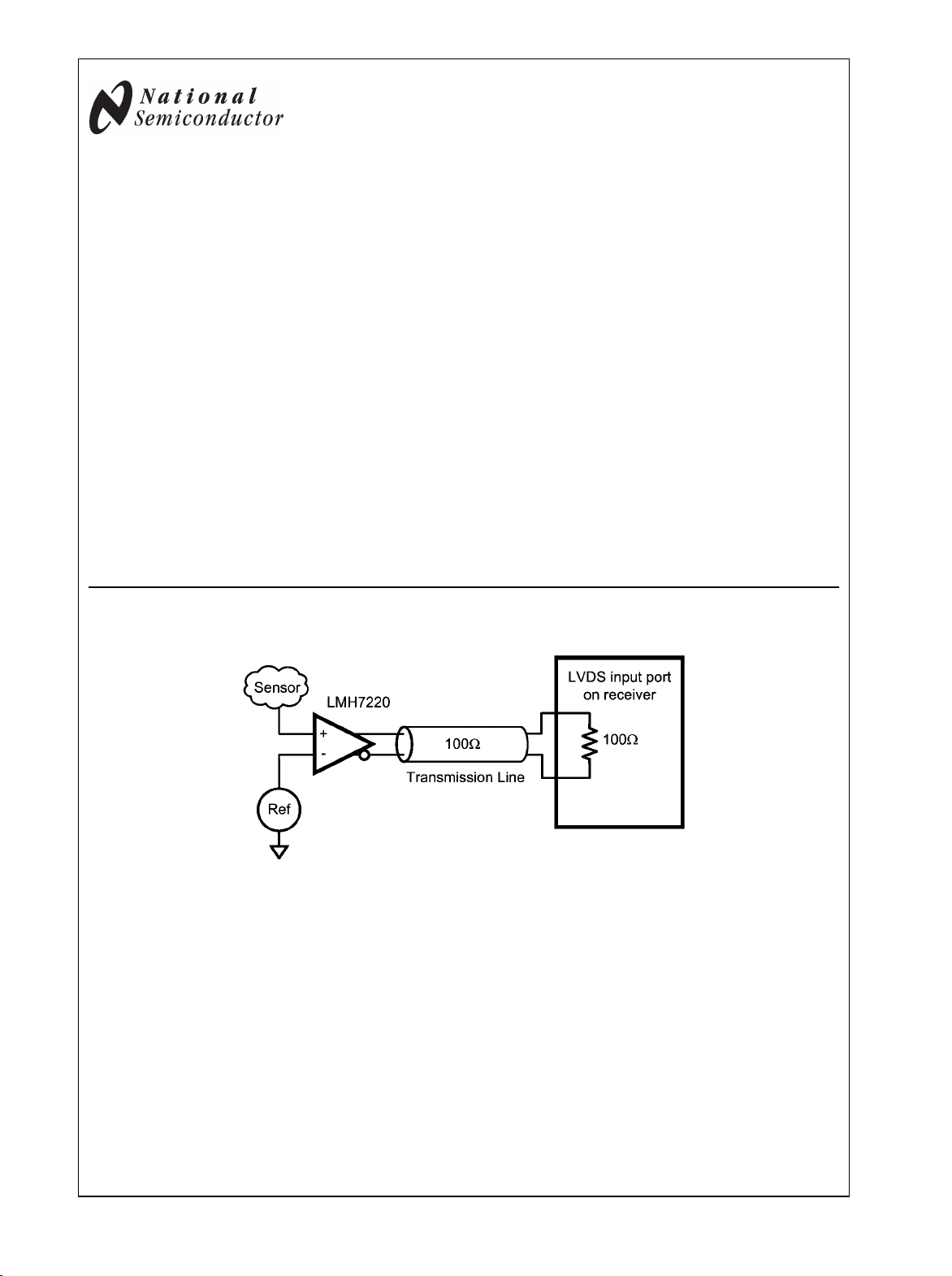
Typical Schematic
Features
(VS = 5V TA = 25°C, Typical values unless otherwise specified)
Propagation delay @ 100 mV overdrive 2.9 ns
■
Rise and fall times 0.6 ns
■
Supply voltage 2.7V to 12V
■
Supply current 6.8 mA
■
Temperature range −40°C to 125°C
■
LVDS output
■
Applications
Acquisition trigger
■
Fast differential line receiver
■
Pulse height analyzer
■
Peak detector
■
Pulse width modulator
■
Remote threshold detection
■
Oscilloscope triggering
■
20137603
© 2007 National Semiconductor Corporation 201376 www.national.com
Absolute Maximum Ratings (Note 1)
If Military/Aerospace specified devices are required,
please contact the National Semiconductor Sales Office/
LMH7220
Distributors for availability and specifications.
ESD Tolerance (Note 2)
Human Body Model 2.5 kV
Machine Model 250V
Supply Voltage (VCC - GND)
Differential Input Voltage ±13V
Output Shorted to GND (Note 4) Continuous
13.5V
Output Shorted Together (Note 4) Continuous
Storage Temperature Range −65°C to +150°C
Voltage on any I/O Pin GND−0.2V to VCC+0.2V
Junction Temperature (Note 3) 150°C max
Operating Ratings (Note 1)
Temperature Range (Note 3) −40°C to +125°C
Supply Voltage 2.7V to 13V
Package Thermal Resistance (θJA )
6-Pin TSOT 189°C/W
+12V DC Electrical Characteristics
Unless otherwise specified, all limits are guaranteed for TJ = 25°C, VCM = 300 mV, −50 mV < VID < +50 mV and RL = 100Ω.
Boldface limits apply at the temperature extremes. (Note 6)
Symbol Parameter Conditions Min
(Note 6)
I
B
Input Bias Current VIN Differential = 0 −5
−7
I
OS
TC I
V
OS
TC V
Input Offset Current VIN Differential = 0 −500 +500 nA
Input Offset Current TC VIN Differential = 0 ±2 nA/°C
OS
Input Offset Voltage −9.5 +9.5 mV
Input Offset Voltage TC ± 50
OS
VRI Input Voltage Range CMRR > 50 dB −0.2 VCC−2 V
CMRR Common-Mode Rejection Ratio VCM = 0 to VCC−2.2V 60 70 dB
PSRR Power Supply Rejection Ratio 63 74 dB
A
V
ΔV
V
V
V
ΔV
I
SC
I
S
V
O
O
OH
OL
OD
OD
Open Loop Gain 59 dB
Output Offset Voltage VIN Differential = 50 mV 1125 1225 1325 mV
VO Change Between ‘0’ and ‘1’ VIN Differential = ±50 mV −25 +25 mV
Output Voltage High VIN Differential = 50 mV 1390 1475 mV
Output Voltage Low VIN Differential = 50 mV 925 1060 mV
Output Voltage Differential VIN Differential = 50 mV 250 330 400 mV
VOD Change between ‘0’ to ‘1’ VIN Differential = ±50 mV −25 +25 mV
Short Circuit Current Output to GND
Pin (Note 4)
Output Shorted Together (Note 4) OUT Q to OUT Q
Supply Current Load Current Excluded
OUT Q to GND Pin
VIN Differential = 50 mV
OUT Q to GND Pin
V
Differential = 50 mV
IN
V
Differential = 50 mV
IN
V
Differential = 50 mV
IN
5
5
5
7.5 10.0
Typ
(Note 5)
(Note 6)
−2.1 −0.5
Max
14.0
Units
µA
μV/°C
mA
mA
+12V AC Electrical Characteristics
Unless otherwise specified, all limits guaranteed for TJ = 25°C, VCM = 300 mV, −50 mV < VID < +50 mV and RL = 100Ω. Boldface limits apply at the temperature extremes. (Note 6)
Symbol Parameter Conditions Min
TR Toggle Rate Overdrive = ±50 mV; CL = 2 pF @
50% Output Swing
t
PDLH
www.national.com 2
Propagation Delay
t
= (t
+ t
PDLH
PDH
PDL
) / 2
(see figure 3 application note)
Input SR = Constant
VID start value = −100 mV
Overdrive 20 mV 3.56
Overdrive 50 mV 2.98
Overdrive 100 mV 2.7 7
Overdrive 1V 2.24
(Note 6)
860 1080 Mb/s
Typ
(Note 5)
Max
(Note 6)
Units
ns
LMH7220
Symbol Parameter Conditions Min
(Note 6)
tOD-disp Input Overdrive Dispersion @Overdrive 20 - 100 mV 0.86
@Overdrive 100 mV - 1V 0.46
tSR-disp Input Slew Rate Dispersion 0.05 V/ns to 1 V/ns
0.24 ns
Typ
(Note 5)
Max
(Note 6)
Units
ns
Overdrive 100 mV
tCM-disp Input Common Mode dispersion SR = 4 V/ns; Overdrive 100 mV
0.55 ns
VCM = 0 to 10V
Δt
Δt
t
t
r
f
PDLH
PDHL
Q to Q Time Skew
| t
- t
PDH
| (Note 8)
PDL
Q to Q Time Skew
| t
- t
PDL
| (Note 8)
PDH
Output Rise Time (20% - 80%) (Note9)Overdrive = 100 mV; CL = 2 pF 0.56 ns
Output Fall Time (20% - 80%) (Note9)Overdrive = 100 mV; CL = 2 pF 0.49 ns
Overdrive = 100 mV; CL = 2 pF 0 ns
Overdrive = 100 mV; CL = 2 pF 0.06 ns
+5V DC Electrical Characteristics
Unless otherwise specified, all limits guaranteed for TJ = 25°C, VCM = 300 mV, −50 mV < VID < +50 mV and RL = 100Ω. Boldface limits apply at the temperature extremes. (Note 6)
Symbol Parameter Conditions Min
(Note 6)
I
B
Input Bias Current VIN Differential = 0 −5
−7
I
OS
TC I
V
OS
TC V
Input Offset Current VIN Differential = 0 −500 +500 nA
Input Offset Current TC VIN Differential = 0 ± 2 nA/°C
OS
Input Offset Voltage −9.5 +9.5 mV
Input Offset Voltage TC ± 50
OS
VRI Input Voltage Range CMRR > 50 dB −0.2 VCC−2 V
CMRR Common-Mode Rejection Ratio VCM = 0 to VCC−2.2V 60 70 dB
PSRR Power Supply Rejection Ratio 63 74 dB
A
V
ΔV
V
V
V
ΔV
I
SC
I
S
V
O
O
OH
OL
OD
OD
Open Loop Gain 59 dB
Output Offset Voltage VIN Differential = 50 mV 1125 1217 1325 mV
VO Change Between ‘0’ and ‘1’ VIN Differential = ±50 mV −25 +25 mV
Output Voltage High VIN Differential = 50 mV 1380 1475 mV
Output Voltage Low VIN Differential = 50 mV 925 1060 mV
Output Voltage Differential VIN Differential = 50 mV 250 320 400 mV
VOD Change between ‘0’ to ‘1’ VIN Differential = ±50 mV −25 +25 mV
Short Circuit Current Output to GND
Pin (Note 4)
Output Shorted Together (Note 4) OUT Q to OUT Q
Supply Current Load Current Excluded
OUT Q to GND Pin
VIN Differential = 50 mV
OUT Q to GND Pin
V
Differential = 50 mV
IN
V
Differential = 50 mV
IN
V
Differential = 50 mV
IN
5
5
5
6.8 9
Typ
(Note 5)
(Note 6)
−1.5 −0.5
Max
12.6
Units
µA
μV/°C
mA
mA
3 www.national.com
+5V AC Electrical Characteristics
Unless otherwise specified, all limits guaranteed for TJ = 25°C, VCM = 300 mV, −50 mV < VID < +50 mV and RL = 100Ω. Bold-
LMH7220
face limits apply at the temperature extremes. (Note 6)
Symbol Parameter Conditions Min
(Note 6)
TR Toggle Rate Overdrive = ±50 mV; CL = 2 pF @
750 940 Mb/s
50% Output Swing
t
PDLH
Propagation Delay
t
= (t
+ t
PDLH
PDH
PDL
) / 2
(see figure 3 application note)
Input SR = Constant
VID start value = -100mV
Overdrive 20 mV 3.63
Overdrive 50 mV 3.09
Overdrive 100 mV 2.9 7
Overdrive 1V 2.41
tOD-disp Input Overdrive Dispersion @Overdrive 20 - 100 mV 0.79
@Overdrive 100 mV - 1V 0.43
tSR-disp Input Slew Rate Dispersion 0.05 V/ns to 1 V/ns
0.20 ns
Overdrive 100 mV
tCM-disp Input Common Mode Dispersion SR = 4 V/ns; Overdrive 100 mV
0.21 ns
VCM = 0 to 3V
Δt
Δt
t
r
PDLH
PDHL
Q to Q Time Skew
| t
- t
PDH
| (Note 8)
PDL
Q to Q Time Skew
| t
- t
PDL
| (Note 8)
PDH
Output Rise Time (20% - 80%) (Note9)Overdrive = 100 mV; CL = 2 pF 0.59 ns
Overdrive = 100 mV; CL = 2 pF 0.09 ns
Overdrive = 100 mV; CL = 2 pF 0.07 ns
Typ
(Note 5)
Max
(Note 6)
Units
ns
ns
t
f
Output Fall Time (20% - 80%) (Note9)Overdrive = 100 mV; CL = 2 pF 0.55 ns
+2.7V DC Electrical Characteristics
Unless otherwise specified, all limits guaranteed for TJ = 25°C, VCM = 300 mV, −50 mV < VID < +50 mV and RL = 100Ω. Boldface limits apply at the temperature extremes. (Note 6)
Symbol Parameter Conditions Min
(Note 6)
I
B
Input Bias Current VIN Differential = 0 −5
−7
I
OS
TC I
V
OS
TC V
Input Offset Current VIN Differential = 0 −500 +500 nA
Input Offset Current TC VIN Differential = 0 ±2 nA/°C
OS
Input Offset Voltage −9.5 +9.5 mV
Input Offset Voltage TC ± 50
OS
VRI Input Voltage Range CMRR > 50 dB −0.2 VCC−2 V
CMRR Common-Mode Rejection Ratio VCM = 0 to VCC−2.2V 56 70 dB
PSRR Power Supply Rejection Ratio 63 74 dB
A
V
ΔV
V
V
O
O
OH
Open Loop Gain 59 dB
Output Offset Voltage VIN Differential = 50 mV 1125 1213 1325 mV
VO Change Between ‘0’ and ‘1’ VIN Differential = ± 50 mV −25 +25 mV
Output Voltage High
VIN Differential = 50 mV 1370 1475 mV
Average of ‘0’ to ‘1’
V
OL
Output Voltage Low
VIN Differential = 50 mV 925 1060 mV
Average of ‘0’ to ‘1’
V
ΔV
OD
OD
Output Voltage Differential VIN Differential = 50 mV 250 315 400 mV
VOD Change between ‘0’ to ‘1’ VIN Differential = ±50 mV −25 +25 mV
Typ
(Note 5)
(Note 6)
−1.3 −0.5
Max
Units
µA
μV/°C
www.national.com 4
LMH7220
Symbol Parameter Conditions Min
(Note 6)
I
SC
Short Circuit Current Output to GND
Pin (Note 4)
OUT Q to GND Pin
VIN Differential = 50 mV
OUT Q to GND Pin
V
Differential = 50 mV
IN
Output Shorted Together (Note 4) OUT Q to OUT Q
V
Differential = 50 mV
IN
I
S
Supply Current Load Current Excluded
V
Differential = 50 mV
IN
5
5
5
6.6 9
Typ
(Note 5)
Max
(Note 6)
12.6
+2.7V AC Electrical Characteristics
Unless otherwise specified, all limits guaranteed for TJ = 25°C, VCM = 300 mV, −50 mV < VID < +50 mV and RL = 100Ω. Boldface limits apply at the temperature extremes. (Note 6)
Symbol Parameter Conditions Min
(Note 6)
TR Toggle Rate Overdrive = ±50 mV; CL = 2 pF @
700 880 Mb/s
50% Output Swing
t
PDLH
Propagation Delay
t
= (t
+ t
PDLH
PDH
PDL
) / 2
(see figure 3 application note)
Input SR = Constant
VID start value = -100mV
Overdrive 20 mV 3.80
Overdrive 50 mV 3.29
Overdrive 100 mV 3.0 7
Overdrive 1V 2.60
tOD-disp Input Overdrive Dispersion @Overdrive 20 - 100 mV 0.83
@Overdrive 100 mV - 1V 0.37
tSR-disp Input Slew Rate Dispersion 0.05 V/ns to 1 V/ns
0.23 ns
Overdrive 100 mV
tCM-disp Input Common Mode dispersion SR = 4 V/ns; Overdrive 100 mV
0.16 ns
VCM = 0 to 1.5V
Δt
PDLH
ΔtPDHL
t
r
Q to Q Time Skew
| t
- t
PDH
| (Note 8)
PDL
Q to Q Time Skew
| t
- t
PDL
| (Note 8)
PDH
Output Rise Time (20% - 80%) (Note9)Overdrive = 100 mV; CL = 2 pF 0.64 ns
Overdrive = 100 mV; CL = 2 pF 0.09 ns
Overdrive = 100 mV; CL = 2 pF 0.09 ns
Typ
(Note 5)
Max
(Note 6)
Units
mA
mA
Units
ns
ns
t
f
Note 1: Absolute Maximum Ratings indicate limits beyond which damage to the device may occur. Operating Conditions indicate specifications for which the
device is intended to be functional, but specific performance is not guaranteed. For guaranteed specifications and the test conditions, see the Electrical
Characteristics.
Note 2: Human Body Model, applicable std. MIL-STD-883, Method 3015.7. Machine Model, applicable std. JESD22-A115-A (ESD MM std. of JEDEC)
Field-Induced Charge-Device Model, applicable std. JESD22-C101-C (ESD FICDM std. of JEDEC)
Note 3: The maximum power dissipation is a function of T
PD = (T
Note 4: Applies to both single-supply and split-supply operation. Continuous short circuit operation at elevated ambient temperature can result in exceeding the
maximum allowed junction temperature of 150°C.
Note 5: Typical values represent the most likely parametric norm as determined at the time of characterization. Actual typical values may vary over time and will
also depend on the application and configuration. The typical values are not tested and are not guaranteed on shipped production material.
Note 6: All limits are guaranteed by testing or statistical analysis.
Note 7: Electrical Table values apply only for factory testing conditions at the temperature indicated. Factory testing conditions result in very limited self-heating
of the device such that TJ = TA. No guarantee of parametric performance is indicated in the electrical tables under conditions of internal self heating where TJ >
TA. See applications section for information on temperature de-rating of this device.
Note 8: Propagation Delay Skew, ΔtPD, is defined as the average of Δt
Note 9: The rise or fall time is the average of the Q and Q
Output Fall Time (20% - 80%) (Note9)Overdrive = 100 mV; CL = 2 pF 0.59 ns
, θJA. The maximum allowable power dissipation at any ambient temperature is
– TA)/ θJA. All numbers apply for packages soldered directly onto a PC Board.
J(MAX)
J(MAX)
PDLH
rise or fall time.
and Δt
.
PDHL
5 www.national.com
Diagrams
LMH7220
Schematic Diagram
Ordering Information
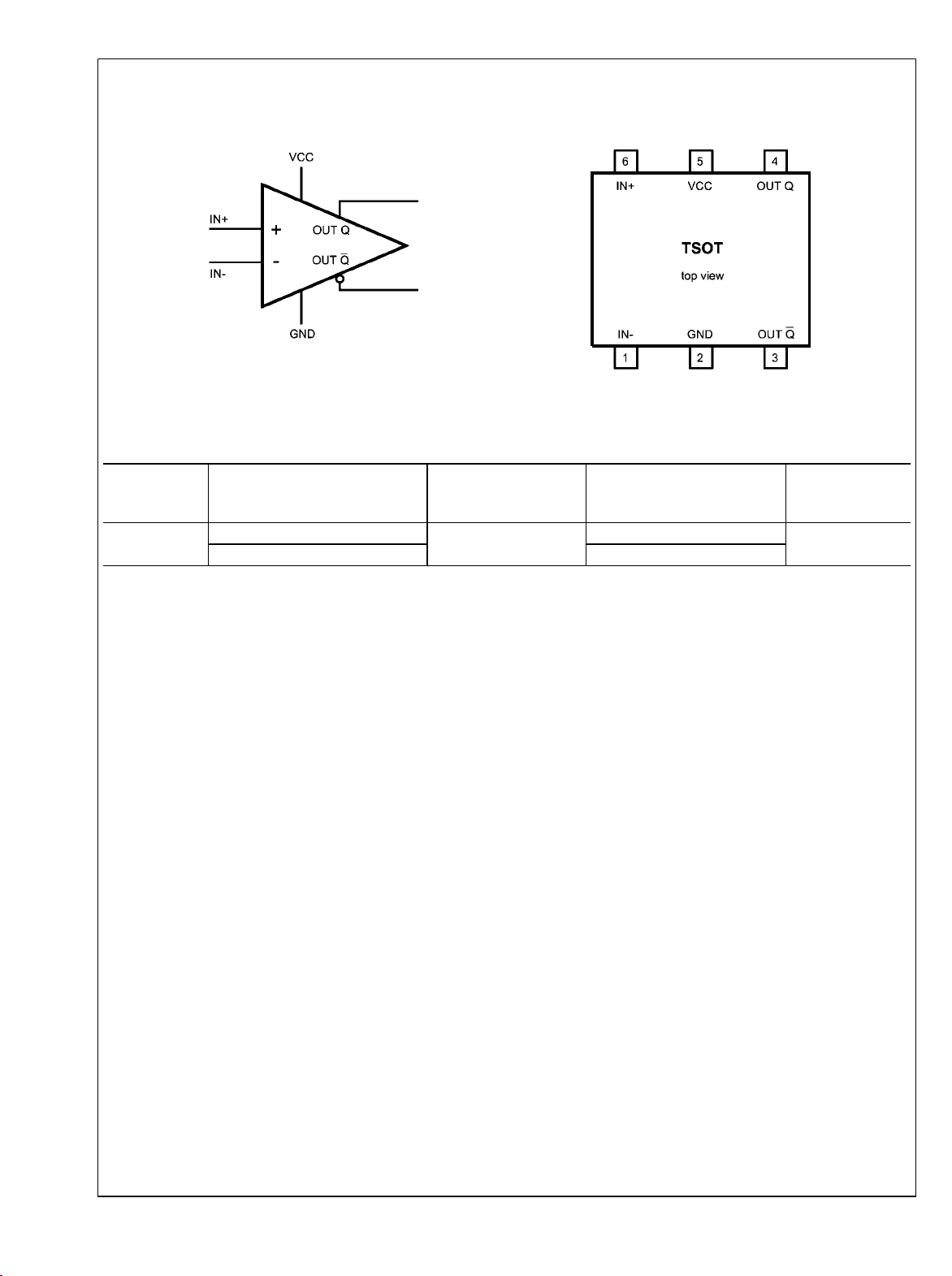
Package Part Number
Temperature Range (TA)
6-Pin TSOT
Connection Diagram
20137601
Package Marking Transport Media NSC Drawing
−40°C to +85°C
LMH7220MK
LMH7220MKX 3k Units Tape and Reel
C29A
1k Units Tape and Reel
20137602
MK06A
www.national.com 6

Typical Performance Characteristics
At TJ = 25°C; unless otherwise specified: VCM = 0.3V, V
OVERDRIVE
LMH7220
= 100 mV, RL = 100Ω.
Input Current vs. Differential Input Voltage
20137621
Bias Current vs. Temperature
Bias Current vs. Supply Voltage
20137636
Output Offset Voltage vs. Supply Voltage
20137623
Output Offset Voltage vs. Temperature
20137625
20137624
Differential Output Voltage vs. Supply Voltage
20137626
7 www.national.com

LMH7220
Differential Output Voltage vs. Temperature
Supply Current vs. Supply Voltage
Supply Current vs. Temperature
Propagation Delay vs. Temperature
20137627
20137629
20137628
Rise & Fall Time vs. Temperature
20137630
Propagation Delay vs. Overdrive Voltage
20137631
www.national.com 8
20137632

LMH7220
Propagation Delay vs. Common Mode Voltage
20137633
Pulse Response Over Temperature
Propagation Delay vs. Slew Rate
20137634
20137635
9 www.national.com

Application Information
INTRODUCTION
LMH7220
The LMH7220 is a high speed comparator with LVDS outputs.
The LVDS (Low Voltage Differential Signaling) standard uses
differential outputs with a voltage swing of approximately 325
mV on each output. The most widely used setup for LVDS
outputs consists of a switched current source of 3.25 mA. The
output pins need to be differentially terminated with an external 100Ω resistor, producing the standardized output voltage
swing of 325 mV. The common mode level of both outputs is
about 1.2V, and is independent of the power supply voltage.
The use of complementary outputs gives a high level of suppression for common mode noise. The very fast rise and fall
times of the LMH7220 enable data transmission rates up to
several hundreds of Megabits per second (Mbps). Due to the
current-nature of the outputs the power consumption remains
at a very low level even if the data transmission rate is rising.
Power delivered to a load resistance of 100Ω is only 1.2 mW.
More information about the LVDS standard can be found on
the National site:
http://www.national.com/appinfo/lvds/0,1798,100,00.html
The LMH7220 inputs have a common mode voltage range
that extends 200 mV below the negative supply voltage thus
allowing ground sensing in case of single supply. The rise and
fall times of the LMH7220 are about 0.6 ns, while the propagation delay time is about 2.7 ns. The LMH7220 can operate
over the full supply voltage range of 2.7V to 12V, while using
single or dual supply voltages. The LVDS outputs refer to the
negative supply rail. The supply current is 6.8 mA at 5V (load
current excluded). The LMH7220 is available in the 6-Pin
TSOT package.
This package is ideal where space is an important issue. In
the next sections the following issues are discussed:
•
In- and output topology
•
Definition of terms of used specifications
•
Propagation delay and dispersion
•
Hysteresis and oscillations
•
The output
•
Applying transmission lines
•
PCB layout
20137610
FIGURE 1. Equivalent Input Circuitry
The output can be seen as a bridge configuration in which
switches are crosswise closed, producing the differential
LVDS logic high and low levels (see Figure 2). The output
switches are fed at top and bottom by two current sources.
The top one is fixed and determines the differential voltage
across the external load resistor. The other one is regulated
and determines the common-mode voltage on the outputs. It
is essential to keep the output common-mode voltage at the
defined standardized LVDS level under all circumstances. To
realize this, both outputs are internally connected together via
two equal resistors. At the midpoint this produces the common mode output voltage, which is made equal to V
by means of the CM feedback loop.
REF
(1.2V)
INPUT & OUTPUT TOPOLOGY
All input and output pins are protected against excessive voltages by ESD diodes. These diodes are connected from the
negative supply to the positive supply. As can be seen in
Figure 1, both inputs are connected to these diodes. Protection against excessive supply voltages is provided by a power
clamp between VCC and GND. Both inputs are also connected
to the bases of the input transistors of the differential pair via
1.5 kΩ resistors. The input transistors cannot withstand high
reverse voltages between bases and emitter, due to their high
frequency properties. To protect the input stage against damage, both bases are connected together by a string of antiparallel diodes. Be aware of situations in which differential
input voltage level is such that these diodes are conducting.
In this case the input current is raised far above the normal
value stated in the datasheet tables.
www.national.com 10
20137611
FIGURE 2. Equivalent Output Circuitry

LMH7220
DEFINITIONS
For a good understanding of many parameters of the
LMH7220 it is necessary to perform a lot of measurements.
All of those parameters are listed in the data tables in the first
part of the datasheet. There are different tables for several
supply voltages containing a separate set of data per supply
voltage. In the table below is a list of abbreviations of the
measured parameters and a short description of the conditions which are applied for measuring them . Following this
table several parameters are highlighted to explain more
clearly what it means exactly and what effects such a phenomena can have for any applied electronic circuit.
Symbol Text Description
I
B
Input Bias Current Current flowing in or out the input pins, when both biased at 0.3 Volt
above GND
I
OS
Input Offset Current Difference between the positive- and the negative input currents
needed to make the outputs change state, averaged for H to L and L
to H transitions
TC I
V
OS
OS
Average Input Offset Current Drift Temperature Coefficient of I
OS
Input Offset Voltage Voltage difference needed between IN+ and IN− to make the outputs
change state, averaged for H to L and L to H transitions
TC V
OS
Average Input Offset Voltage Drift Temperature Coefficient of V
OS
CMRR Common Mode Rejection Ratio Ratio of input offset voltage change and input common mode voltage
change
VRI Input Voltage Range Upper and lower limits of the input voltage are defined as where
CMRR drops below 50 dB.
PSRR Power Supply Rejection Ratio Ratio of input offset voltage change and supply voltage change from
V
to V
S-MIN
V
O
Output Offset Voltage Output Common Mode Voltage averaged for logic ‘0’ and logic ‘1’
S-MAX
levels (See Figure 12)
ΔV
O
Change in Output Offset Voltage Difference in Output Common Mode Voltage between logic ‘0’ and
logic ‘1’ levels (See Figure 13)
V
V
V
V
V
ΔV
OH
OL
ODH
ODL
OD
OD
Output Voltage High High state single ended output voltage (Q or Q) (See Figure 12)
Output Voltage Low Low state single ended output voltage (Q or Q) (See Figure 12)
Output Differential Voltage logic ‘1’ V
Output Differential Voltage logic ‘0’ V
Average of V
ODH
and V
ODL
Change in VOD between ‘0’ and ‘1’ |V
OH(Q)
OH(Q)
(V
ODH
ODH
– V
OL(Q)
– V
OL(Q)
+ V
ODL
– V
| (See Figure 13)
ODL
(logic level ‘1’) (See Figure 13)
(logic level ‘0’) (See Figure 13)
) / 2
Hyst Hysteresis Difference in input switching levels for L to H and H to L transitions.
(See Figure 11)
I
SQG
, I
SQG
Short Circuit Current one output to
Current that flows from one output to GND if shorted single ended
GND
I
SQQ
Short Circuit Current outputs together Current flowing between output Q and output Q if shorted differentially
TR Maximum Toggle Rate Maximum frequency at which the outputs can toggle before VOD drops
under 50% of the nominal value.
PW Pulse Width Time from 50% of the rising edge of a signal to 50% of the falling edge
t
PDH
resp t
PDL
Propagation Delay Delay time between the moment the input signal crosses the switching
level L to H and the moment the output signal crosses 50% of the
rising edge of Q output (t
), or delay time between the moment the
PDH
input signal crosses the switching level H to L and the moment the
t
PDL
resp t
PDH
output signal crosses 50% of the falling edge of Q output (t
Delay time between the moment the input signal crosses the switching
PDL
)
level L to H and the moment the output signal crosses 50% of the
falling edge of Q output (t
), or delay time between the moment the
PDL
input signal crosses the switching level H to L and the moment the
t
PDLH
t
PDHL
t
PD
output signal crosses 50% of the rising edge of Q output (t
Average of t
Average of t
Average of t
PDH
PDL
PDLH
and t
and t
and t
PDL
PDH
PDHL
PDH
)
11 www.national.com

t
PDHd
LMH7220
Δt
PDLH
Δt
PD
Δt
PDd
t
OD-disp
t
SR-disp
t
CM-disp
tr / t
rd
tf / t
fd
Symbol Text Description
resp t
PDLd
Delay time between the moment the input signal crosses the switching
level L to H and the zero crossing of the rising edge of the differential
output signal (t
), or delay time between the moment the input
PDHd
signal crosses the switching level H to L and the zero crossing of the
falling edge of the differential output signal (t
resp Δt
Q to Q time skew Time skew between 50% levels of rising edge of Q output and falling
PDHL
edge of Q output (Δt
), or time skew between 50% levels of falling
PDLH
edge of Q output and rising edge of Q output (Δt
Average Q to Q time skew Average of t
Average diff. time skew Average of t
PDLH
PDHd
and t
and t
for L to H and H to L transients
PDHL
for L to H and H to L transients
PDLd
Input overdrive dispersion Change in tPD for different overdrive voltages at the input pins
Input slew rate dispersion Change in tPD for different slew rates at the input pins
Input Common Mode dispersion Change in tPD for different common mode voltages at the input pins
Output rise time (20% - 80%) Time needed for the (single ended or differential) output voltage to
change from 20% of its nominal value to 80%
Output fall time (20% - 80%) Time needed for the (single ended or differential) output voltage to
change from 80% of its nominal value to 20%
PDLd
)
PDHL
)
FIGURE 3. Propagation Delay Definition
DELAY AND DISPERSION
Comparators are widely used to connect the analog world to
the digital one. The accuracy of a comparator is dictated by
its DC properties such as offset voltage and hysteresis and
by its timing aspects such as rise and fall times and delay. For
low frequency applications most comparators are much faster
than the analog input signals they handle. The timing aspects
are less important here than the accuracy of the input switching levels. The higher the frequency, the more important the
timing properties of the comparator become, because the response of the comparator can give e.g. a noticeable change
in time frame or duty cycle. A designer has to know these
effects in order to deal with them. In order to predict what the
output signal will do compared to the input signal, several parameters are defined which describe the behavior of the
www.national.com 12
20137620
comparator. For a good understanding of the timing parameters discussed in the following section, a brief explanation is
given and several timing diagrams are shown for clarification.
PROPAGATION DELAY
The propagation delay parameter is defined as the time it
takes for the comparator to change the output level halfway
in its transition from L to H or H to L, in reaction to the moment
the input signal crosses the switching level. Due to this definition there are two parameters, t
parameters don’t necessarily have the same value. It is pos-
PDH
and t
(Figure 4). Both
PDL
sible that differences will occur due to a different response of
the internal circuitry. As a result of this effect another parameter is defined: ΔtPD. This parameter is defined as the absolute value of the difference between t
PDH
and t
PDL
.

20137604
FIGURE 4. Pulse Parameter
If ΔtPD isn’t zero, duty cycle distortion will occur. For example
when applying a symmetrical waveform (e.g. a sinewave) at
the input, it is expected that the comparator produces a symmetrical square wave at the output with a duty cycle of 50%.
In case of different t
signal will not remain at 50%, but will be lower or higher. In
PDH
and t
the duty cycle of the output
PDL
addition to the propagation delay parameters for single ended
outputs discussed before, there are other parameters in case
of complementary outputs. These parameters describe the
delay from input to each of the outputs and the difference between both delay times (see Figure 5). When the differential
input signal crosses the reference level from L to H, both outputs will switch to their new state with some delay. This is
defined as t
the difference between both signals is defined as ΔtP
similar definitions for the falling slope of the input signal can
for the Q output and t
PDH
for the Q output, while
PDL
DLH
be seen in Figure 3.
LMH7220
Both output circuits should be symmetrical. At the moment
one output is switching ‘on’ the other is switching ‘off’ with
ideally no skew between them. The design of the LMH7220
is optimized to minimize this timing difference. Propagation
delay tPD is defined as the average delay of both outputs at
both slopes: (t
DISPERSION
There are several circumstances that will produce a variation
of the propagation delay time. This effect is called dispersion.
Amplitude Overdrive Dispersion
One of the parameters that causes dispersion is the amplitude
variation of the input signal. Figure 6 shows the dispersion
due to a variation of the input overdrive voltage. The overdrive
is defined as the ‘goto’ differential voltage applied to the inputs. Figure 6 shows the impact it has on the propagation
delay time if overdrive is varied from 10 millivolts to 100 millivolts. This parameter is measured with a constant slew rate
of the input signal.
.
PDLH
+ t
PDHL
) / 2.
FIGURE 5. Propagation Delay
20137607
FIGURE 6. Overdrive Dispersion
The overdrive dispersion is caused by the fact that switching
currents in the input stage depend on the level of the differential input signal.
Slew Rate Dispersion
The slew rate is another parameter that affects propagation
delay. The higher the input slew rate, the faster the input stage
switches (Figure 7).
20137612
13 www.national.com

LMH7220
FIGURE 7. Slew Rate Dispersion
A combination of overdrive- and slew rate dispersion occurs
when applying signals with different amplitude at constant
frequency. A small amplitude will produce a small voltage
change per time unit (dV/dt) but also a small maximum switching current (overdrive) in the input transistors. High amplitudes produce a high dV/dt and a bigger overdrive.
Common Mode Dispersion
Dispersion will also occur when changing the common mode
level of the input signal (Figure 8). When V
through the CMVR (Common Mode Voltage Range), this results in a variation of the propagation delay time. This variation is called Common Mode Dispersion.
20137608
is swept
REF
All of the dispersion effects discussed before influence the
propagation delay. In practice the dispersion is often caused
by a combination of more than one varied parameter. It is
good to realize this if there is the need to predict how much
dispersion a circuit will show.
HYSTERESIS & OSCILLATIONS
In contrast to an op amp, the output of a comparator has only
two defined states ‘0’ or ‘1’. Due to finite comparator gain
however, there will be a small band of input differential voltage
where the output is in an undefined state. An input signal with
fast slopes will pass this band very quickly without problems.
During slow slopes however, passing the band of uncertainty
can be relatively long. This enables the comparator outputs
to switch back and forth several times between ‘0’ and ‘1’ on
a single slope. The comparator will switch on its input noise,
ground bounce (possible oscillations), ringing etc. Noise in
the input signal will also contribute to these undesired switching effects.
In the next sections an explanation follows about these phenomena in situations where no hysteresis is applied, and the
possible improvement hysteresis can give.
Using No Hysteresis
In Figure 9 can be seen what happens when the input signal
rises from just under the threshold V
it. From the moment the input reaches the lowest dotted line
around V
ends when the input signal leaves the undefined area at t=1.
at t=0, the output toggles on noise etc. Toggling
REF
to a level just above
REF
In this example the output was fast enough to toggle three
times. Due to this behavior digital circuitry connected to the
output will count a wrong number of pulses. One way to prevent this is to choose a very slow comparator with an output
that is not able to switch more than once between ‘0’ and ‘1’
during the time the input state is undefined.
20137609
FIGURE 8. Common Mode Dispersion
www.national.com 14
20137614
FIGURE 9. Oscillations & Noise
In most circumstances this is not an option because the slew
rate of the input signal will vary.

LMH7220
Using Hysteresis
A good way to avoid oscillations and noise during slow slopes
is the use of hysteresis. For this purpose a threshold is introduced that pushes the input switching level back at the moment the output switches (See Figure 10). In this simple
setup, a comparator with a single output and a resistive divider to the positive input is drawn.
20137613
FIGURE 10. Simplified Schematic
The divider RF-RP feeds back a portion of the output voltage
to the positive input. Only a small part of the output voltage is
needed, just enough to avoid the area at which the input is in
an undefined state. Assuming this is only a few millivolts, it is
sufficient to add (plus or minus) 10 mV to the positive input to
prevent the circuit from oscillations. If the output switches between 0V and 5V and the choice for one of the resistors is
done the other can be calculated. Assume RP is 50Ω then
RF is 25 kΩ for 10 mV threshold on the positive input. The
situation of Figure 11 is now created.
to level B. So before the output has the possibility to toggle
again, the difference between both inputs is made sufficient
to have a stable situation again. When the input signal comes
down from high to low, the situation is stable until level B is
reached at t=0. At this moment the output will toggle back,
and the circuit is back in the start situation with the negative
input at a much lower level than the positive one. In the situation without hysteresis, the output would toggle exactly at
V
. With hysteresis this happens at the introduced levels A
REF
and B, as can be seen in Figure 11. Varying the levels A and
B will also vary the timing of t=0 and t=1. When designing a
circuit be aware of this effect. Introducing hysteresis will
cause some time shifts between output and input (e.g. duty
cycle variations), but eliminates undesired switching of the
output.
Parasitic Capacitors
In the simple schematic of Figure 10 some capacitors are
drawn. The capacitors CP. represent the parasitic (board) capacitance at the input of the part. This capacity will slow down
the change of the level of the positive input in reaction to the
changing output voltage. As a result of this, the output may
have the time to switch over more than once. Actually the
parasitic capacity represented by CP makes the attenuation
circuit of RF and RP frequency dependent. The only action to
take is to create a frequency independent circuit. This is simply done by placing the compensation capacitor CC in parallel
with RF. The capacitor CC can be calculated with the formula
RF *CC = RP *CP, this means that both of the time constants
must be the same to create a frequency independent network.
A simple example gives the following assuming that CP is in
total 2.5 pF and as already calculated RF = 25 kΩ in combination with RP = 50Ω. These input data gives:
CC = RP * CP/R
CC = 50*2.5e-12/25e3
F
CC = 5e-15 = 0.005 pF
This is not a practical value and different conclusions are
possible:
•
No capacitor CC needed
•
Place a capacitor CC of 1 pF and accept a big overshoot
at the positive input being sure that the input stage is in a
secure new position
•
Place an extra CP of such a value that CC has a realistic
value of say 1 pF (extra CP = ±500 pF).
20137615
FIGURE 11. Hysteresis
In this picture there are two dotted lines A and B, both indicating the resulting level at the positive input. When the signal
at the negative input is low, the state of the input stage is well
defined with the negative input much lower than the positive
input. As a result the output will be in the high state. The positive input is at level A. With the input signal sloping up, this
situation remains until VIN crosses level A at t=1. Now the
output toggles, and the voltage at the positive input is lowered
Position of Feedback Resistors
Another important issue while using positive feedback is the
placement of the resistors RP and RF. These resistors must
be placed as near as possible to the positive input, because
this input is most sensitive for picking up spurious signals,
noise etc. This connection must be very clean for the best
performance of the overall circuit. With raising speeds the total PCB design becomes more and more critical, the
LMH7220 comparator doesn’t have built in hysteresis, so the
input signal must meet minimum requirements to make the
output switch over properly. In the following sections some
aspects concerning the load connected to the outputs and
transmission lines will be discussed.
THE OUTPUT SWING PROPERTIES
LVDS has differential outputs which means that both outputs
have the same swing but in opposite direction (Figure 12).
Both outputs swing around a voltage called the common
mode output voltage (VO). This voltage can be measured at
the midpoint of two equal resistors connected to both outputs
as discussed in the section ‘Input and Output Topology’. The
15 www.national.com

absolute value of the difference between both voltages is
called VOD. LVDS outputs cannot be held at the VO level because of their digital nature. They only cross this level during
LMH7220
a transition. Due to the symmetrical structure of the circuit,
both output voltages cross at VO regardless if the output
changes from ‘0’ to ‘1’ or vise versa.
FIGURE 12. LVDS Output Signals
In case the outputs aren’t symmetrical or are a-symmetrically
loaded, the output voltages differ from the situation of Figure
12. For this non-ideal situation there are two additional parameters defined, ΔVO and ΔVOD, as can be seen in Figure
13.
comparator’s outputs. In the case of a balanced input connected to the load resistance, current IP is drawn from both
output connection points to ground. Keep in mind that the
LMH7220’s ability to source currents is much higher than to
sink them. The connected input circuitry also forms a differential load to the outputs of the comparator (see Figure 14).
This will cause the voltage across the termination resistor to
differ from its nominal value.
20137605
20137616
FIGURE 14. Load
20137606
FIGURE 13. LVDS Output Signals with Different
Amplitude
ΔVO is the difference in VO between the ‘1’ state and the ‘0’
state. This variation is acceptable if it is below 50 mV following
the ANSI/TIA/EIA-644 LVDS standard. It is also possible that
VOD in the ‘1’ state isn’t the same as in the ‘0’ state. This parameter is specified as ΔVOD, and is calculated as the absolute value of the difference of V
ODH
and V
ODL
.
LOADING THE OUTPUT
The output structure creates a current (I
through an external differential load resistor of 100Ω nominal.
see Figure 14)
LOOP
This results in a differential output voltage of 325 mV. The
outputs of the comparator are connected to tracks on a PCB.
These tracks can be seen as a differential transmission line.
The differential load resistor acts as a high frequency termination at the end of the transmission line. This means that for
a proper signal behavior the PCB tracks have to be dimensioned for a characteristic impedance of 100Ω as well.
Changing the load resistor also implies a change of the transmission line impedance. More about transmission lines and
termination can be found in the next section. The signal
across the 100Ω termination resistor is fed into the inputs of
subsequent circuitry that processes the data. Any connection
to input circuitry of course draws current from the
In general one single connection only draws a few µA’s, and
doesn’t have much effect on the LVDS output voltage. For
multiple inputs on one output pair, load currents must not exceed the specified limits, as described in the ANSI or IEEE
LVDS standards. Below a specified value of VOD, the functioning of subsequent circuitry becomes uncertain. However
under normal conditions there is no need to worry. Another
point of practice is load capacitances. Capacitances are applied differentially (C
capacitors will disturb the pulse shape. The edges of the out-
) and also to ground (CP). All of these
LOAD
put pulse become slower, and in reaction the detection of the
transition comes at a later moment. Be aware of this effect
when measuring with probes. Both single ended and differential probes have these capacitances. A standard probe
commonly has a load capacity of about 8 to 10 pF. This will
cause some degradation of the pulse shape and will add
some time delay.
TRANSMISSION LINES & TERMINATION TECHNOLOGIES
The LMH7220 uses LVDS technology. LVDS is a way to communicate data using low voltage swing and low power consumption. Nowadays data rates are growing, requiring
increasing speed. Data isn’t only connected to other IC’s on
a single PCB board but in many cases there are interconnections from board to board or from equipment to equipment.
Distances can be short or long but it is always necessary to
have a reliable connection, consume low power and to be able
to handle high data rates. LVDS is a differential signal protocol. The advantage over single ended signal transmission is
its higher immunity to common mode noise. Common mode
signals are signals that are equally apparent on both lines and
because the receiver only looks at the difference between
both lines, this noise is canceled.
www.national.com 16

LMH7220
Maximum Bitrates
A very important specification in high speed circuits are the
rise and fall times. In fact these determine the maximum toggle rate (TR) of the part. The LVDS standard specifies them
at 0.26 ns to 1.5 ns. Rise and fall times are normally specified
at 20% and 80% of the signal amplitude (60% difference). In
order to know what the maximum toggle rate is , it is required
to recalculate the rise- and fall times to 100% swing in stead
of 60%. TR is defined as the bitrate at which the differential
output voltage drops to 50% of its nominal value. TR can be
calculated from the rise & fall times:
TR=60/50 * 2/(Tr + Tf)
So the fastest rise / fall (0.26 ns both) leads to:
max. TR=60/50 * 2e9/(0.26 + 0.26) = 4.62 Gb/s
The slowest edges (1.5 ns both) yield:
min. TR=60/50 * 2e9/(1.5 + 1.5) = 0.8 Gb/s
Other types of transmission lines are the strip line and the
micro strip. These last types are used on PCB boards. They
have the characteristic impedance dictated by the physical
dimensions of a track placed over a metal ground plane (See
Figure 17).
20137617
FIGURE 15. Bitrate
Need for Terminated Transmission Lines
During the ‘80’s and ‘90’s National fabricated the 100k ECL
logic family. The rise and fall time specification was 0.75 ns
which was very fast and will easily introduce errors in digital
circuits if insufficient care has been taken to the transmission
lines and terminations used for these signals. To be helpful to
designers that use ECL with “old” PCB-techniques, the 10k
ECL family was introduced with a rise and fall time specification of 2 ns. This was much slower and more easy to use.
LVDS signals have transition times that exceed the fastest
ECL family. A careful PCB design is needed using RF techniques for transmission and termination. Transmission lines
can be formed in several ways. The most commonly used
types are the coaxial cable and the twisted pair telephony cable (Figure 16).
20137618
FIGURE 16. Cable Configuration
These cables have a characteristic impedance determined by
their geometric parameters. Widely used impedances for the
coaxial cable are 50Ω and 75Ω. Twisted pair cables have
impedances of about 120Ω to 150Ω.
20137619
FIGURE 17. PCB Transmission Lines
Differential Microstrip Line
The transmission line which is ideally suited for LVDS signals
is the differential micro strip line. This is a double micro strip
line with a narrow space in between. This means both lines
have a strong coupling and this determines mainly the characteristic impedance. The fact that they are routed above a
copper plane doesn't affect differential impedance, only CMcapacitance is added. Each of the structures above has its
own geometric parameters so for each structure there is another formula to calculate the right impedance. For calculations of these transmission lines visit the National website or
feel free to order the RAPIDESIGNER. For some formula’s
given in the ‘LVDS owners manual’ see chapter 3 (see the
‘Introduction’ section for the URL). At the end of the transmission line there must be a termination having the same
impedance as of the transmission line itself. It doesn’t matter
what impedance the line has, if the load has the same value
no reflections will occur. When designing a PCB board with
transmission lines on it, space becomes an important item
especially on high density boards. With a single micro strip
line, line width is fixed for given impedance and a board material. Other line widths will result in different impedances.
Advantage of Differential Microstrip
Impedances of transmission lines are always dictated by their
geometric parameters. This is also true for differential micro
strip lines. Using this type of transmission lines, track distance
determines mainly the resulting impedance. So, if the PCB
manufacturer can produce reliable boards with narrow track
spacing the track width for a given impedance is also small.
17 www.national.com

The wider the spacing, the wider tracks are needed for a certain impedance. For example two tracks of 0.2 mm width and
0.1 mm spacing have the same impedance as two tracks of
LMH7220
0.8 mm width and 0.4 mm spacing. With high-end PCB processes, it is possible to design very narrow differential microstrip transmission lines. It is desirable to use these
phenomena to create optimal connections to the receiving
part or the terminating resistor, in accordance with their physical dimensions. Seen from the comparator, the termination
resistor must be connected at the far end of the line. Open
connections after the termination resistor (e.g. to an input of
a receiver) must be as short as possible. The allowed length
of such connections varies with the received transients. The
faster the transients the shorter open lines must be to prevent
signal degradation.
PCB LAYOUT CONSIDERATIONS AND COMPONENT VALUES SELECTION
High frequency designs require that both active- and passive
components are selected that are specially designed for this
purpose. The LMH7220 is fabricated in two different small
packages intended for surface mount design. For reliable high
speed design it is highly recommended also to use small surface mount passive components because these packages
have low parasitic capacitance and low inductance simply
because they have no leads to connect them to the PCB. It is
possible to amplify signals at frequencies of several hundreds
of MHz using standard through- hole resistors. Surface mount
devices however are better suited for this purpose. Another
important issue is the PCB itself, which is no longer a simple
carrier for all the parts and a medium to interconnect them.
The PCB becomes a real component itself and consequently
contributes its own high frequency properties to the overall
performance of the circuit. Practice dictates that a high frequency design at least has one ground plane, providing a low
impedance path for all decoupling capacitors and other
ground connections. Care should be taken especially that onboard transmission lines have the same impedance as the
cables to which they are connected. Most single ended applications have 50Ω impedance (75Ω for video and cable TV
applications). On PCBs, such low impedance single ended
microstrip transmission lines usually require much wider
traces (2 to 3 mm) on a standard double sided PCB board
than needed for a ‘normal’ trace. Another important issue is
that inputs and outputs shouldn’t ‘see’ each other. This occurs
if input- and output tracks are routed in parallel over the PCB
with only a small amount of physical separation, and particularly when the difference in signal level is high. Furthermore
components should be placed as flat and low as possible on
the surface of the PCB. For higher frequencies a long lead
can act as a coil, a capacitor or an antenna. A pair of leads
can even form a transformer. Careful design of the PCB minimizes oscillations, ringing and other unwanted behavior. For
ultra high frequency designs only surface mount components
will give acceptable results. (for more information see OA-15).
NSC suggests the following evaluation boards as a guide for
high frequency layout and as an aid in device testing and
characterization.
LMH730220 / 551012993-002 Rev A
www.national.com 18

Physical Dimensions inches (millimeters) unless otherwise noted
LMH7220
NS Package Number MK06A
6-Pin TSOT
19 www.national.com

Notes
THE CONTENTS OF THIS DOCUMENT ARE PROVIDED IN CONNECTION WITH NATIONAL SEMICONDUCTOR CORPORATION
(“NATIONAL”) PRODUCTS. NATIONAL MAKES NO REPRESENTATIONS OR WARRANTIES WITH RESPECT TO THE ACCURACY
OR COMPLETENESS OF THE CONTENTS OF THIS PUBLICATION AND RESERVES THE RIGHT TO MAKE CHANGES TO
SPECIFICATIONS AND PRODUCT DESCRIPTIONS AT ANY TIME WITHOUT NOTICE. NO LICENSE, WHETHER EXPRESS,
IMPLIED, ARISING BY ESTOPPEL OR OTHERWISE, TO ANY INTELLECTUAL PROPERTY RIGHTS IS GRANTED BY THIS
DOCUMENT.
LMH7220 High Speed Comparator with LVDS Output
TESTING AND OTHER QUALITY CONTROLS ARE USED TO THE EXTENT NATIONAL DEEMS NECESSARY TO SUPPORT
NATIONAL’S PRODUCT WARRANTY. EXCEPT WHERE MANDATED BY GOVERNMENT REQUIREMENTS, TESTING OF ALL
PARAMETERS OF EACH PRODUCT IS NOT NECESSARILY PERFORMED. NATIONAL ASSUMES NO LIABILITY FOR
APPLICATIONS ASSISTANCE OR BUYER PRODUCT DESIGN. BUYERS ARE RESPONSIBLE FOR THEIR PRODUCTS AND
APPLICATIONS USING NATIONAL COMPONENTS. PRIOR TO USING OR DISTRIBUTING ANY PRODUCTS THAT INCLUDE
NATIONAL COMPONENTS, BUYERS SHOULD PROVIDE ADEQUATE DESIGN, TESTING AND OPERATING SAFEGUARDS.
EXCEPT AS PROVIDED IN NATIONAL’S TERMS AND CONDITIONS OF SALE FOR SUCH PRODUCTS, NATIONAL ASSUMES NO
LIABILITY WHATSOEVER, AND NATIONAL DISCLAIMS ANY EXPRESS OR IMPLIED WARRANTY RELATING TO THE SALE
AND/OR USE OF NATIONAL PRODUCTS INCLUDING LIABILITY OR WARRANTIES RELATING TO FITNESS FOR A PARTICULAR
PURPOSE, MERCHANTABILITY, OR INFRINGEMENT OF ANY PATENT, COPYRIGHT OR OTHER INTELLECTUAL PROPERTY
RIGHT.
LIFE SUPPORT POLICY
NATIONAL’S PRODUCTS ARE NOT AUTHORIZED FOR USE AS CRITICAL COMPONENTS IN LIFE SUPPORT DEVICES OR
SYSTEMS WITHOUT THE EXPRESS PRIOR WRITTEN APPROVAL OF THE CHIEF EXECUTIVE OFFICER AND GENERAL
COUNSEL OF NATIONAL SEMICONDUCTOR CORPORATION. As used herein:
Life support devices or systems are devices which (a) are intended for surgical implant into the body, or (b) support or sustain life and
whose failure to perform when properly used in accordance with instructions for use provided in the labeling can be reasonably expected
to result in a significant injury to the user. A critical component is any component in a life support device or system whose failure to perform
can be reasonably expected to cause the failure of the life support device or system or to affect its safety or effectiveness.
National Semiconductor and the National Semiconductor logo are registered trademarks of National Semiconductor Corporation. All other
brand or product names may be trademarks or registered trademarks of their respective holders.
Copyright© 2007 National Semiconductor Corporation
For the most current product information visit us at www.national.com
www.national.com
National Semiconductor
Americas Customer
Support Center
Email:
new.feedback@nsc.com
Tel: 1-800-272-9959
National Semiconductor Europe
Customer Support Center
Fax: +49 (0) 180-530-85-86
Email: europe.support@nsc.com
Deutsch Tel: +49 (0) 69 9508 6208
English Tel: +49 (0) 870 24 0 2171
Français Tel: +33 (0) 1 41 91 8790
National Semiconductor Asia
Pacific Customer Support Center
Email: ap.support@nsc.com
National Semiconductor Japan
Customer Support Center
Fax: 81-3-5639-7507
Email: jpn.feedback@nsc.com
Tel: 81-3-5639-7560
 Loading...