

查询LMH6715供应商
LMH6715
Dual Wideband Video Op Amp
LMH6715 Dual Wideband Video Op Amp
January 2003
General Description
The LMH6715 combines National’s VIP10™high speed
complementary bipolar process with National’s current feedback topology to produce a very high speed dual op amp.
The LMH6715 provides 400MHz small signal bandwidth at a
gain of +2V/V and 1300V/µs slew rate while consuming only
5.8mA per amplifier from
The LMH6715 offers exceptional video performance with its
0.02% and 0.02˚ differential gain and phase errors for NTSC
and PAL video signals while driving up to four back terminated 75Ω loads. The LMH6715 also offers a flat gain response of 0.1dB to 100MHz and very low channel-tochannel crosstalk of −70dB at 10MHz. Additionally, each
amplifier can deliver 70mA of output current. This level of
performance makes the LMH6715 an ideal dual op amp for
high density, broadcast quality video systems.
The LMH6715’s two very well matched amplifiers support a
number of applications such as differential line drivers and
receivers. In addition, the LMH6715 is well suited for Sallen
Key active filters in applications such as anti-aliasing filters
for high speed A/D converters. Its small 8-pin SOIC package,
low power requirement, low noise and distortion allow the
LMH6715 to serve portable RF applications such as IQ
channels.
±
5V supplies.
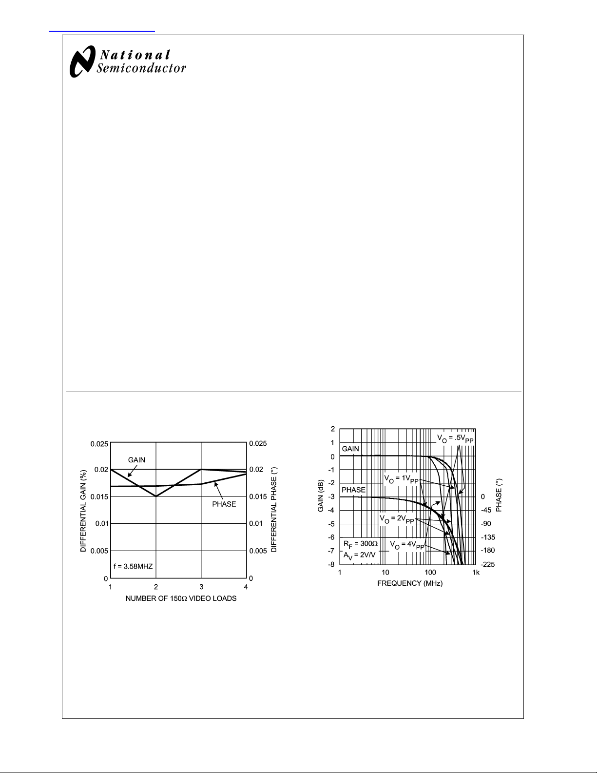
Differential Gain & Phase with
Multiple Video Loads
Features
TA= 25˚C, RL= 100Ω, typical values unless specified.
n Very low diff. gain, phase: 0.02%, 0.02˚
n Wide bandwidth: 480MHz (A
+2V/V)
n 0.1dB gain flatness to 100MHz
n Low power: 5.8mA/channel
n −70dB channel-to-channel crosstalk (10MHz)
n Fast slew rate: 1300V/µs
n Unity gain stable
n Improved replacement for CLC412
= +1V/V); 400MHz (AV=
V
Applications
n HDTV, NTSC & PAL video systems
n Video switching and distribution
n IQ amplifiers
n Wideband active filters
n Cable drivers
n DC coupled single-to-differential conversions
Frequency Response vs. V
OUT
20042916
20042908
© 2003 National Semiconductor Corporation DS200429 www.national.com
Absolute Maximum Ratings (Note 1)
If Military/Aerospace specified devices are required,
please contact the National Semiconductor Sales Office/
LMH6715
Storage Temperature Range −65˚C to +150˚C
Lead Temperature (Soldering 10
sec)
Distributors for availability and specifications.
ESD Tolerance (Note 4)
Operating Ratings
Human Body Model 2000V
Machine Model 150V
±
V
CC
I
OUT
Common-Mode Input Voltage
6.75V
(Note 3)
±
V
CC
Differential Input Voltage 2.2V
Thermal Resistance
Package (θ
)(θJA)
JC
SOIC 65˚C/W 145˚C/W
Operating Temperature Range −40˚C to +85˚C
Nominal Operating Voltage
Maximum Junction Temperature +150˚C
Electrical Characteristics
AV= +2, RF= 500Ω,VCC=±5V,RL= 100Ω; unless otherwise specified. Boldface limits apply at the temperature extremes.
Symbol Parameter Conditions Min Typ Max Units
Frequency Domain Response
SSBW -3dB Bandwidth V
LSBW -3dB Bandwidth V
Gain Flatness V
GFP Peaking DC to 100MHz, RF= 300Ω 0.1 dB
GFR Rolloff DC to 100MHz, R
LPD Linear Phase Deviation DC to 100MHz, R
DG Differential Gain R
DP Differential Phase R
Time Domain Response
Tr Rise and Fall Time 0.5V Step 1.4 ns
Ts Settling Time to 0.05% 2V Step 12 ns
OS Overshoot 0.5V Step 1 %
SR Slew Rate 2V Step 1300 V/µs
Distortion And Noise Response
HD2 2nd Harmonic Distortion 2V
HD3 3rd Harmonic Distortion 2V
Equivalent Input Noise
V
N
I
N
I
NN
Non-Inverting Voltage
Inverting Current
Non-Inverting Current
SNF Noise Floor
XTLKA Crosstalk Input Referred 10MHz −70 dB
Static, DC Performance
V
DV
I
BN
DI
I
BI
DI
IO
IO
BN
BI
Input Offset Voltage
Average Drift
Input Bias Current Non-Inverting
Average Drift
Input Bias Current Inverting
Average Drift
PSRR Power Supply Rejection Ratio DC 46
<
0.5VPP,RF= 300Ω 280 400 MHz
OUT
<
4.0VPP,RF= 300Ω 170 MHz
OUT
<
0.5V
OUT
= 150Ω, 4.43MHz 0.02 %
L
= 150Ω, 4.43MHz 0.02 deg
L
PP
= 300Ω 0.1 dB
F
= 300Ω 0.25 deg
F
4V Step 3 ns
, 20MHz −60 dBc
PP
, 20MHz −75 dBc
PP
>
1MHz 3.4 nV/
>
1MHz 10.0 pA/
>
1MHz 1.4 pA/
>
1MHz −153 dB
±
2
±
30 µV/˚C
±
5
±
30 nA/˚C
±
6
±
20 nA/˚C
±
6
±
8
±
12
±
20
±
21
±
35
60 dB
44
+300˚C
±
5V to±6V
mV
1Hz
µA
µA
www.national.com 2
Electrical Characteristics (Continued)
AV= +2, RF= 500Ω,VCC=±5V,RL= 100Ω; unless otherwise specified. Boldface limits apply at the temperature extremes.
Symbol Parameter Conditions Min Typ Max Units
CMRR Common Mode Rejection Ratio DC 50
47
I
CC
Supply Current per Amplifier RL=
∞
4.7
4.1
Miscellaneous Performance
R
IN
C
IN
R
OUT
V
O
V
OL
Input Resistance Non-Inverting 1000 kΩ
Input Capacitance Non-Inverting 1.0 pF
Output Resistance Closed Loop .06 Ω
Output Voltage Range RL=
∞
RL= 100Ω
±
3.5
±
3.4
CMIR Input Voltage Range Common Mode
I
O
Note 1: Absolute Maximum Ratings indicate limits beyond which damage to the device may occur. Operating Ratings indicate conditions for which the device is
intended to be functional, but specific performance is not guaranteed. For guaranteed specifications, see the Electrical Characteristics tables.
Note 2: Electrical Table values apply only for factory testing conditions at the temperature indicated. Factory testing conditions result in very limited self-heating of
the device such that T
See Applications Section for information on temperature de-rating of this device." Min/Max ratings are based on product characterization and simulation. Individual
parameters are tested as noted.
Note 3: The maximum output current (I
more details.
Note 4: Human body model, 1.5kΩ in series with 100pF. Machine model, 0Ω In series with 200pF.
Output Current 70 mA
. No guarantee of parametric performance is indicated in the electrical tables under conditions of internal self heating where T
J=TA
) is determined by device power dissipation limitations. See the Power Dissipation section of the Application Division for
OUT
56 dB
5.8 7.6
8.1
±
4.0 V
±
3.9 V
±
2.2 V
mA
J
LMH6715
>
TA.
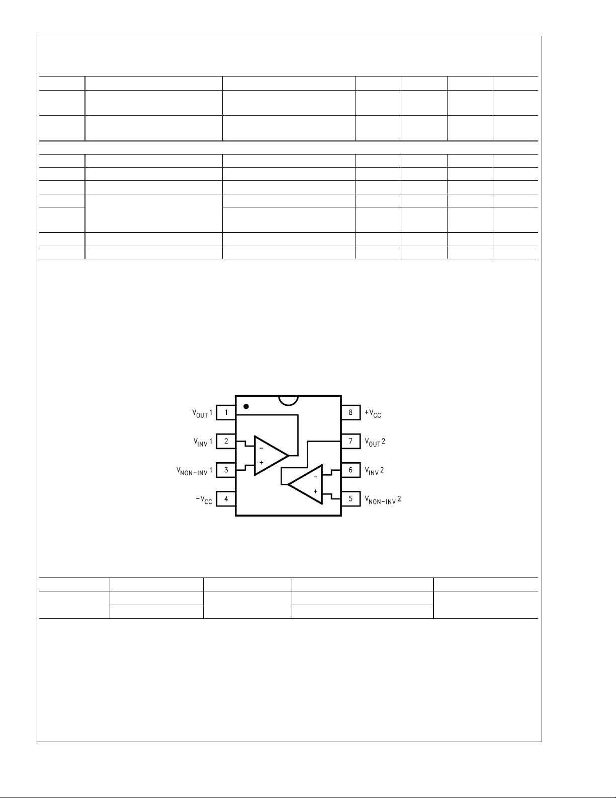
Connection Diagram
8-Pin SOIC
Top View
20042904
Ordering Information
Package Part Number Package Marking Transport Media NSC Drawing
8-pin SOIC
LMH6715MA
LMH6715MAX 2.5k Units Tape and Reel
LMH6715MA
Rails
M08A
www.national.com3
Typical Performance Characteristics (T
100Ω, unless otherwise specified).
LMH6715
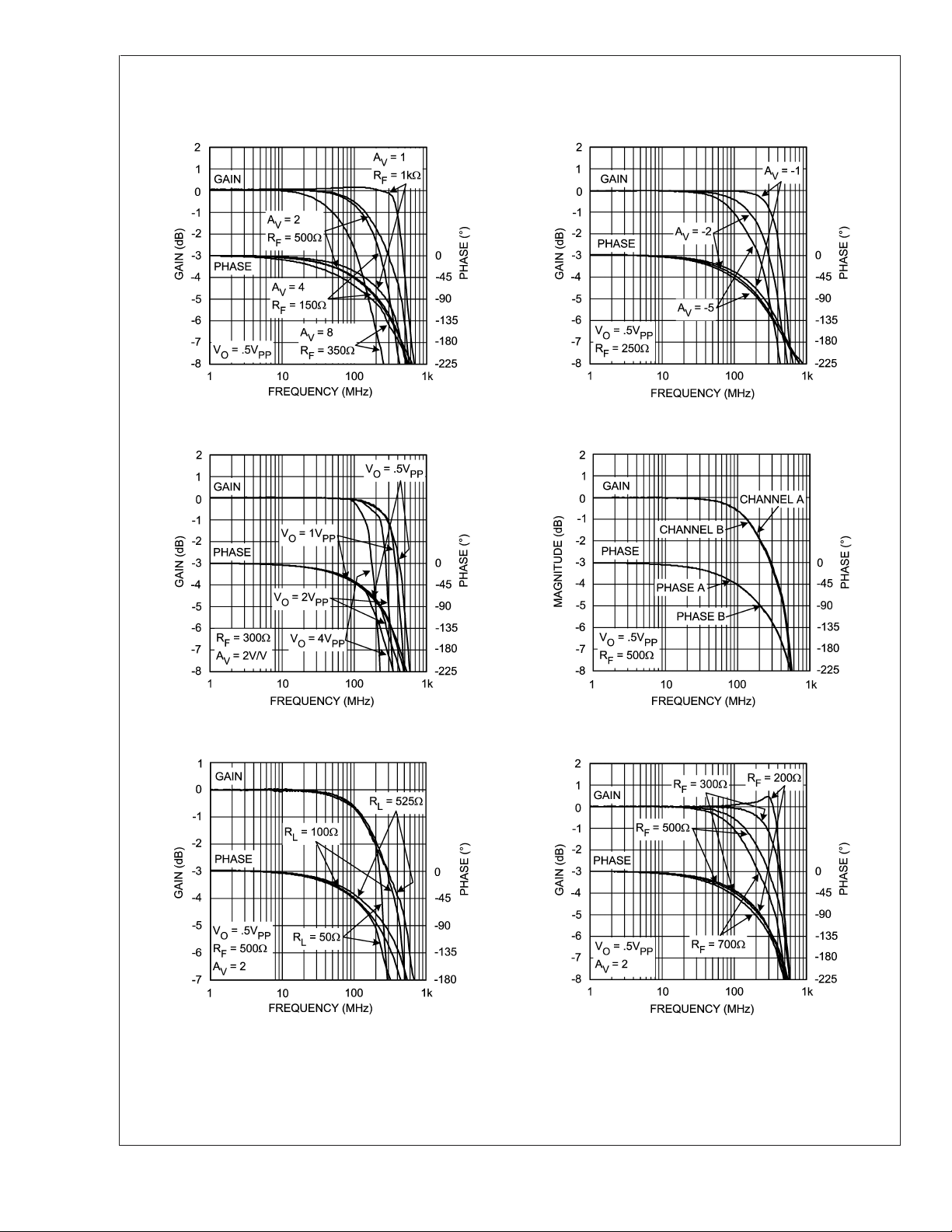
Non-Inverting Frequency Response Inverting Frequency Response
= 25˚C, VCC=±5V, AV=±2V/V, RF= 500Ω,RL=
A
20042913
Non-Inverting Frequency Response vs. V
OUT
20042916 20042901
Small Signal Channel Matching
Frequency Response vs. Load Resistance Non-Inverting Frequency Response vs. R
20042912
F
20042915
www.national.com 4
20042914

LMH6715
Typical Performance Characteristics (T
unless otherwise specified). (Continued)
Small Signal Pulse Response Large Signal Pulse Response
20042918 20042919
Input-Referred Crosstalk Settling Time vs. Accuracy
= 25˚C, VCC=±5V, AV=±2V/V, RF= 500Ω,RL= 100Ω,
A
−3dB Bandwidth vs. V
OUT
20042907
20042925
20042924
DC Errors vs. Temperature
20042926
www.national.com5

Typical Performance Characteristics (T
unless otherwise specified). (Continued)
LMH6715
Open Loop Transimpedance, Z(s) Equivalent Input Noise vs. Frequency
Differential Gain & Phase vs. Load Differential Gain vs. Frequency
= 25˚C, VCC=±5V, AV=±2V/V, RF= 500Ω,RL= 100Ω,
A
20042920 20042923
20042908
Differential Phase vs. Frequency Gain Flatness & Linear Phase Deviation
20042910
www.national.com 6
20042909
20042911

LMH6715
Typical Performance Characteristics (T
= 25˚C, VCC=±5V, AV=±2V/V, RF= 500Ω,RL= 100Ω,
A
unless otherwise specified). (Continued)
2nd Harmonic Distortion vs. Output Voltage 3rd Harmonic Distortion vs. Output Voltage
20042902 20042905
Closed Loop Output Resistance PSRR & CMRR
Suggested RSvs. C
20042906 20042917
L
20042927
www.national.com7

Application Section
LMH6715
FIGURE 1. Non-Inverting Configuration with Power
Supply Bypassing
20042935
FEEDBACK RESISTOR SELECTION
One of the key benefits of a current feedback operational
amplifier is the ability to maintain optimum frequency response independent of gain by using appropriate values for
the feedback resistor (R
Typical Performance plots specify an R
±
+2V/V and
5V power supplies (unless otherwise specified).
Generally, lowering R
). The Electrical Characteristics and
F
from it’s recommended value will
F
of 500Ω, a gain of
F
peak the frequency response and extend the bandwidth
while increasing the value of R
response to roll off faster. Reducing the value of R
will cause the frequency
F
too far
F
below it’s recommended value will cause overshoot, ringing
and, eventually, oscillation.
Frequency Response vs. R
F
20042937
FIGURE 2. Inverting Configuration with Power Supply
Bypassing
Application Introduction
Offered in an 8-pin package for reduced space and cost, the
wideband LMH6715 dual current-feedback op amp provides
closely matched DC and AC electrical performance characteristics making the part an ideal choice for wideband signal
processing. Applications such as broadcast quality video
systems, IQ amplifiers, filter blocks, high speed peak detectors, integrators and transimedance amplifiers will all find
superior performance in the LMH6715 dual op amp.
20042914
The plot labeled “Frequency Response vs. RF” shows the
LMH6715’s frequency response as R
= +2). This plot shows that an RFof 200Ω results in
A
V
peaking and marginal stability. An R
is varied (RL= 100Ω,
F
of 300Ω gives near
F
maximal bandwidth and gain flatness with good stability, but
>
with very light loads (R
peaking. An R
of 500Ω gives excellent stability with good
F
300Ω) the device may show some
L
bandwidth and is the recommended value for most applications. Since all applications are slightly different it is worth
some experimentation to find the optimal R
for a given
F
circuit. For more information see Application Note OA-13
which describes the relationship between R
and closed-
F
loop frequency response for current feedback operational
amplifiers.
When configuring the LMH6715 for gains other than +2V/V,
it is usually necessary to adjust the value of the feedback
resistor. The two plots labeled “R
and “R
vs. Inverting Gain” provide recommended feedback
F
vs. Non-inverting Gain”
F
resistor values for a number of gain selections.
www.national.com 8

Application Introduction (Continued)
R
vs. Non-Inverting Gain
F
20042921
Both plots show the value of RFapproaching a minimum
value (dashed line) at high gains. Reducing the feedback
resistor below this value will result in instability and possibly
oscillation. The recommended value of R
solid line, which begins to increase at higher gains. The
reason that a higher R
need to keep R
G
is required at higher gains is the
F
from decreasing too far below the output
impedance of the input buffer. For the LMH6715 the output
resistance of the input buffer is approximately 160Ω and 50Ω
is a practical lower limit for R
. Due to the limitations on R
G
the LMH6715 begins to operate in a gain bandwidth limited
±
fashion for gains of
5V/V or greater.
R
vs. Inverting Gain
F
is depicted by the
F
LMH6715
tances (to AC ground) arising from traces or pads placed too
closely (
due to the frequency response peaking caused by these
parasitics, a small adjustment of the feedback resistor value
will serve to compensate the frequency response. Also, it is
very important to keep the parasitic capacitance across the
feedback resistor to an absolute minimum.
The performance plots in the data sheet can be reproduced
using the evaluation boards available from National. The
CLC730036 board uses all SMT parts for the evaluation of
the LMH6715. The board can serve as an example layout for
the final production printed circuit board.
Care must also be taken with the LMH6715’s layout in order
to achieve the best circuit performance, particularly channelto-channel isolation. The decoupling capacitors (both tantalum and ceramic) must be chosen with good high frequency
characteristics to decouple the power supplies and the
physical placement of the LMH6715’s external components
is critical. Grouping each amplifier’s external components
with their own ground connection and separating them from
the external components of the opposing channel with the
maximum possible distance is recommended. The input
(R
also recommended that the ceramic decoupling capacitor
(0.1µF chip or radial-leaded with low ESR) should be placed
as closely to the power pins as possible.
POWER DISSIPATION
Follow these steps to determine the Maximum power dissipation for the LMH6715:
G
1. Calculate the quiescent (no-load) power: P
-VEE)
2. Calculate the RMS power at the output stage: P
-V
current across the external load.
3. Calculate the total RMS power: Pt = P
The maximum power that the LMH6715, package can dissi-
pate at a given temperature can be derived with the following
equation:
Pmax = (150
ture (˚C) and θ
ambient, for a given package (˚C/W). For the SOIC package
θ
<
0.1”) to power or ground planes. In some cases,
) and gain setting resistors (RF) are the most critical. It is
IN
AMP=ICC(VCC
)(I
LOAD
is 145˚C/W.
JA
), where V
LOAD
o
- Tamb)/ θJA, where Tamb = Ambient tempera= Thermal resistance, from junction to
JA
LOAD
and I
are the voltage and
LOAD
AMP+PO
O
=(V
CC
20042922
When using the LMH6715 as a replacement for the CLC412,
identical bandwidth can be obtained by using an appropriate
value of R
that an R
. The chart “Frequency Response vs. RF” shows
F
of approximately 700Ω will provide bandwidth
F
very close to that of the CLC412. At other gains a similar
increase in R
can be used to match the new and old parts.
F
CIRCUIT LAYOUT
With all high frequency devices, board layouts with stray
capacitances have a strong influence over AC performance.
The LMH6715 is no exception and its input and output pins
are particularly sensitive to the coupling of parasitic capaci-
MATCHING PERFORMANCE
With proper board layout, the AC performance match between the two LMH6715’s amplifiers can be tightly controlled
as shown in Typical Performance plot labeled “Small-Signal
Channel Matching”.
The measurements were performed with SMT components
using a feedback resistor of 300Ω at a gain of +2V/V.
The LMH6715’s amplifiers, built on the same die, provide the
advantage of having tightly matched DC characteristics.
SLEW RATE AND SETTLING TIME
One of the advantages of current-feedback topology is an
inherently high slew rate which produces a wider full power
bandwidth. The LMH6715 has a typical slew rate of 1300V/
µs. The required slew rate for a design can be calculated by
the following equation: SR = 2πfV
.
pk
Careful attention to parasitic capacitances is critical to
achieving the best settling time performance. The LMH6715
www.national.com9

Application Introduction (Continued)
has a typical short term settling time to 0.05% of 12ns for a
LMH6715
2V step. Also, the amplifier is virtually free of any long term
thermal tail effects at low gains.
When measuring settling time, a solid ground plane should
be used in order to reduce ground inductance which can
cause common-ground-impedance coupling. Power supply
and ground trace parasitic capacitances and the load capacitance will also affect settling time.
Placing a series resistor (R
mended for optimal settling time performance when driving a
capacitive load. The Typical Performance plot labeled “R
and Settling Time vs. Capacitive Load” provides a means for
selecting a value of R
DC & NOISE PERFORMANCE
A current-feedback amplifier’s input stage does not have
equal nor correlated bias currents, therefore they cannot be
canceled and each contributes to the total DC offset voltage
at the output by the following equation:
The input resistance is the resistance looking from the noninverting input back toward the source. For inverting DCoffset calculations, the source resistance seen by the input
resistor R
must be included in the output offset calculation
g
as a part of the non-inverting gain equation. Application note
OA-7 gives several circuits for DC offset correction. The
noise currents for the inverting and non-inverting inputs are
graphed in the Typical Performance plot labeled “Equivalent
Input Noise”. A more complete discussion of amplifier inputreferred noise and external resistor noise contribution can be
found in OA-12.
DIFFERENTIAL GAIN & PHASE
The LMH6715 can drive multiple video loads with very low
differential gain and phase errors. The Typical Performance
plots labeled “Differential Gain vs. Frequency” and “Differential Phase vs. Frequency” show performance for loads from
1 to 4. The Electrical Characteristics table also specifies
performance for one 150Ω load at 4.43MHz. For NTSC
video, the performance specifications also apply. Application
note OA-24 “Measuring and Improving Differential Gain &
Differential Phase for Video”, describes in detail the techniques used to measure differential gain and phase.
) at the output pin is recom-
s
for a given capacitive load.
s
Applications Circuits
SINGLE-TO-DIFFERENTIAL LINE DRIVER
The LMH6715’s well matched AC channel-response allows a
single-ended input to be transformed to highly matched
push-pull driver. From a 1V single-ended input the circuit of
Figure 3 produces 1V differential signal between the two
20042945
=
1
outputs. For larger signals the input voltage divider (R
) is necessary to limit the input voltage on channel 2.
2R
2
S
FIGURE 3. Single-to-Differential Line Driver
DIFFERENTIAL LINE RECEIVER
Figure 4 and Figure 5 show two different implementations of
an instrumentation amplifier which convert differential signals to single-ended. Figure 5 allows CMRR adjustment
through R
.
2
I/O VOLTAGE & OUTPUT CURRENT
The usable common-mode input voltage range (CMIR) of
the LMH6715 specified in the Electrical Characteristics table
±
of the data sheet shows a range of
2.2 volts. Exceeding
this range will cause the input stage to saturate and clip the
output signal.
The output voltage range is determined by the load resistor
±
and the choice of power supplies. With
output driver will typically drive
±
5 volts the class A/B
3.9V into a load resistance
of 100Ω. Increasing the supply voltages will change the
common-mode input and output voltage swings while at the
same time increase the internal junction temperature.
www.national.com 10
20042946
FIGURE 4. Differential Line Receiver

LMH6715
Applications Circuits (Continued)
20042947
FIGURE 5. Differential Line Receiver with CMRR
Adjustment
NON-INVERTING CURRENT-FEEDBACK INTEGRATOR
The circuit of Figure 6 achieves its high speed integration by
placing one of the LMH6715’s amplifiers in the feedback
loop of the second amplifier configured as shown.
LOW NOISE WIDE-BANDWIDTH TRANSIMPEDANCE
AMPLIFIER
Figure 7 implements a low noise transimpedance amplifier
using both channels of the LMH6715. This circuit takes
advantage of the lower input bias current noise of the noninverting input and achieves negative feedback through the
second LMH6715 channel. The output voltage is set by the
value of R
through the adjustment of R
while frequency compensation is achieved
F
.
T
20042950
FIGURE 7. Low-Noise, Wide Bandwidth,
Transimpedance Amp.
20042949
FIGURE 6. Current Feedback Integrator
www.national.com11

Physical Dimensions inches (millimeters)
unless otherwise noted
LMH6715 Dual Wideband Video Op Amp
8-Pin SOIC
NS Package Number M08A
LIFE SUPPORT POLICY
NATIONAL’S PRODUCTS ARE NOT AUTHORIZED FOR USE AS CRITICAL COMPONENTS IN LIFE SUPPORT
DEVICES OR SYSTEMS WITHOUT THE EXPRESS WRITTEN APPROVAL OF THE PRESIDENT AND GENERAL
COUNSEL OF NATIONAL SEMICONDUCTOR CORPORATION. As used herein:
1. Life support devices or systems are devices or
systems which, (a) are intended for surgical implant
into the body, or (b) support or sustain life, and
whose failure to perform when properly used in
accordance with instructions for use provided in the
2. A critical component is any component of a life
support device or system whose failure to perform
can be reasonably expected to cause the failure of
the life support device or system, or to affect its
safety or effectiveness.
labeling, can be reasonably expected to result in a
significant injury to the user.
National Semiconductor
Americas Customer
Support Center
Email: new.feedback@nsc.com
Tel: 1-800-272-9959
www.national.com
National does not assume any responsibility for use of any circuitry described, no circuit patent licenses are implied and National reserves the right at any time without notice to change said circuitry and specifications.
National Semiconductor
Europe Customer Support Center
Fax: +49 (0) 180-530 85 86
Email: europe.support@nsc.com
Deutsch Tel: +49 (0) 69 9508 6208
English Tel: +44 (0) 870 24 0 2171
Français Tel: +33 (0) 1 41 91 8790
National Semiconductor
Asia Pacific Customer
Support Center
Fax: 65-6250 4466
Email: ap.support@nsc.com
Tel: 65-6254 4466
National Semiconductor
Japan Customer Support Center
Fax: 81-3-5639-7507
Email: nsj.crc@jksmtp.nsc.com
Tel: 81-3-5639-7560
 Loading...