

查询LMH6714供应商
LMH6714/6720/6722
Wideband Video Op Amp; Single, Single with Shutdown
and Quad
LMH6714/6720/6722 Wideband Video Op Amp; Single, Single with Shutdown and Quad
March 2003
General Description
The LMH6714/6720/6722 series combine National’s
™
VIP10
National’s current feedback topology to produce a very high
speed op amp. These amplifiers provide a 400MHz small
signal bandwidth at a gain of +2V/V and a 1800V/µs slew
rate while consuming only 5.6mA from
The LMH6714/6720/6722 series offer exceptional video performance with its 0.01% and 0.01˚ differential gain and
phase errors for NTSC and PAL video signals while driving a
back terminated 75Ω load. They also offer a flat gain response of 0.1dB to 120MHz. Additionally, they can deliver
70mA continuous output current. This level of performance
makes them an ideal op amp for broadcast quality video
systems.
The LMH6714/6720/6722’s small packages (SOIC &
SOT23), low power requirement, low noise and distortion
allow the LMH6714/6720/6722 to serve portable RF applications. The high impedance state during shutdown makes the
LMH6720 suitable for use in multiplexing multiple high speed
signals onto a shared transmission line. The LMH6720 is
also ideal for portable applications where current draw can
be reduced with the shutdown function.
high speed complementary bipolar process with
±
5V supplies.
Features
n 400MHz (AV= +2V/V, V
n 250MHz (A
n 0.1dB gain flatness to 120MHz
n Low power: 5.6mA
n TTL compatible shutdown pin (LMH6720)
n Very low diff. gain, phase: 0.01%, 0.01˚ (LMH6714)
n −58 HD2/ −70 HD3 at 20MHz
n Fast slew rate: 1800V/µs
n Low shutdown current: 500uA (LMH6720)
n 11ns turn on time (LMH6720)
n 7ns shutdown time (LMH6720)
n Unity gain stable
n Improved replacement for CLC400,401,402,404,406 and
446 (LMH6714)
n Improved replacement for CLC405 (LMH6720)
n Improved replacement for CLC415 (LMH6722)
= +2V/V, V
V
= 500mVPP) −3dB BW
OUT
=2VPP) -3dB BW
OUT
Applications
n HDTV, NTSC & PAL video systems
n Video switching and distribution
n Wideband active filters
n Cable drivers
n High speed multiplexer (LMH6720)
n Programmable gain amplifier (LMH6720)
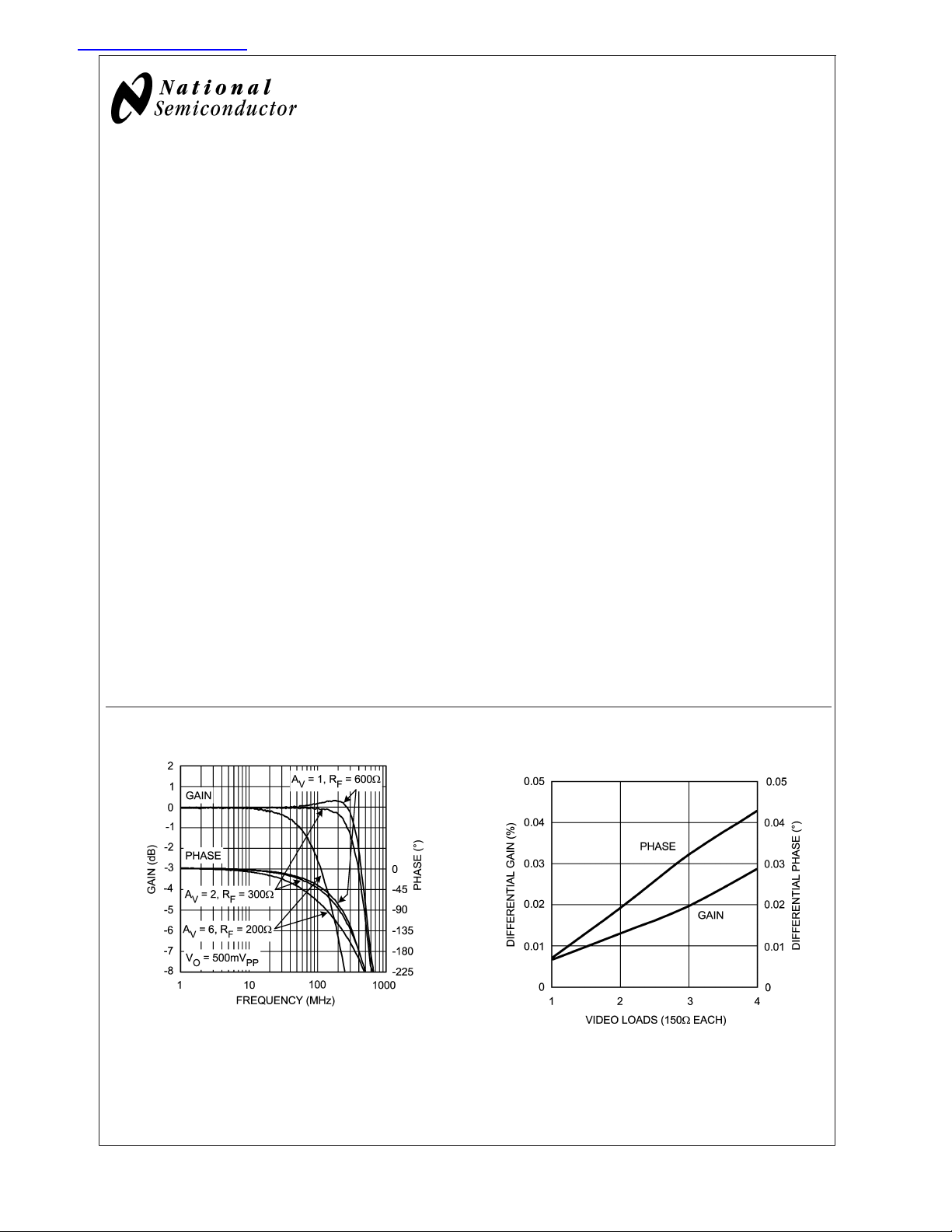
Non-Inverting Small Signal Frequency Response
20056506
© 2003 National Semiconductor Corporation DS200565 www.national.com
Differential Gain and Phase vs. Number of Video
Loads (LMH6714)
20056528
Absolute Maximum Ratings (Note 1)
If Military/Aerospace specified devices are required,
Storage Temperature Range −65˚C to +150˚C
Shutdown Pin Voltage (Note 5) +V
to VCC/2-1V
CC
please contact the National Semiconductor Sales Office/
Distributors for availability and specifications.
Operating Ratings (Note 3)
ESD Tolerance (Note 4)
Human Body Model 2000V
LMH6714/6720/6722
Machine Model 200V
V
CC
I
OUT
Common Mode Input Voltage
Differential Input Voltage 2.2V
Maximum Junction Temperature +150˚C
Storage Temperature Range −65˚C to +150˚C
Lead Temperature (soldering 10 sec) +300˚C
±
6.75V
(Note 3)
±
V
CC
Thermal Resistance
Package (θ
5-Pin SOT23 232˚C/W
6-Pin SOT23 198˚C/W
8-Pin SOIC 145˚C/W
14-Pin SOIC 130˚C/W
Operating Temperature −40˚C +85˚C
Nominal Supply Voltage
±
5V
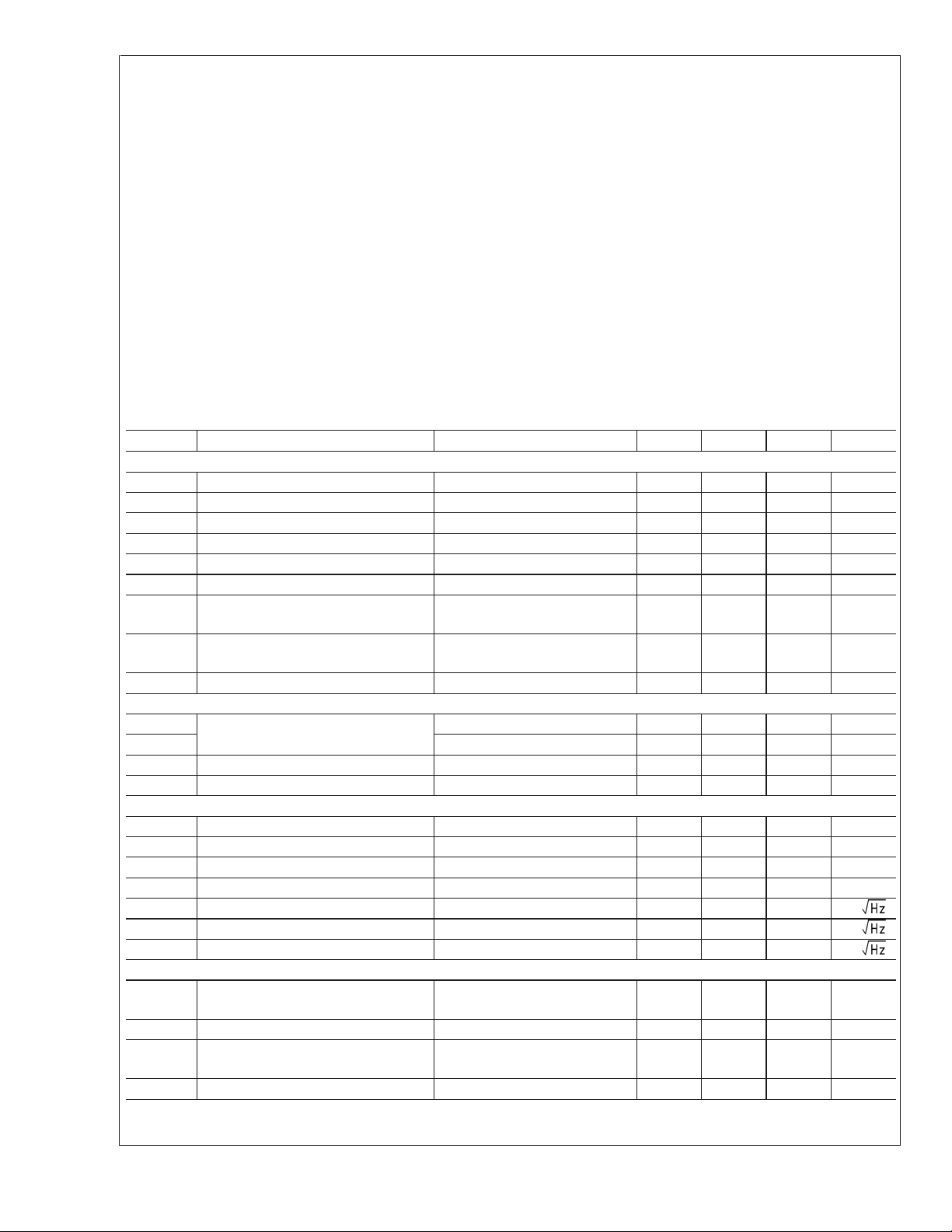
Electrical Characteristics
Unless specified, AV= +2, RF= 300Ω:VCC=±5V, RL= 100Ω, LMH6714/6720/6722. Boldface limits apply at temperature
extremes.
Symbol Parameter Conditions Min Typ Max Units
Frequency Domain Response
SSBW −3dB Bandwidth V
LSBW −3dB Bandwidth V
Gain Flatness V
GFP Peaking DC to 120MHz 0.1 dB
GFR Rolloff DC to 120MHz 0.1 dB
LPD Linear Phase Deviation DC to 120MHz 0.5 deg
DG Differential Gain R
DG Differential Gain R
DP Differential Phase RL= 150Ω, 4.43MHz 0.01 deg
Time Domain Response
TRS Rise and Fall Time .5V Step 1.5 ns
TRL 2V Step 2.6 ns
t
s
Settling Time to 0.05% 2V Step 12 ns
SR Slew Rate 6V Step 1200 1800 V/µs
Distortion and Noise Response
HD2 2nd Harmonic Distortion 2V
HD3 3rd Harmonic Distortion 2V
IMD 3rd Order Intermodulation Products 10MHz, P
Equivalent Input Noise
VN Non-Inverting Voltage
NICN Inverting Current
ICN Non-Inverting Current
Static, DC Performance
V
IO
Output Offset Voltage
DVIO Average Drift 8 µV/˚C
I
BN
Input Bias Current Non-Inverting
DIBN Average Drift 4 nA/˚C
= 0.5V
OUT
OUT
OUT
= 150Ω, 4.43MHz
L
= 2.0V
=2V
PP
PP
PP
345 400 MHz
200 250 MHz
0.01 %
(LMH6714)
= 150Ω, 4.43MHz
L
0.02 %
(LMH6720)
, 20MHz −58 dBc
PP
, 20MHz −70 dBc
PP
= 0dBm −78 dBc
OUT
>
1MHz 3.4 nV/
>
1MHz 10 pA/
>
1MHz 1.2 pA/
±
0.2
±
1
±
6
±
8
±
10
±
15
)
JA
±
6V
mV
µA
www.national.com 2
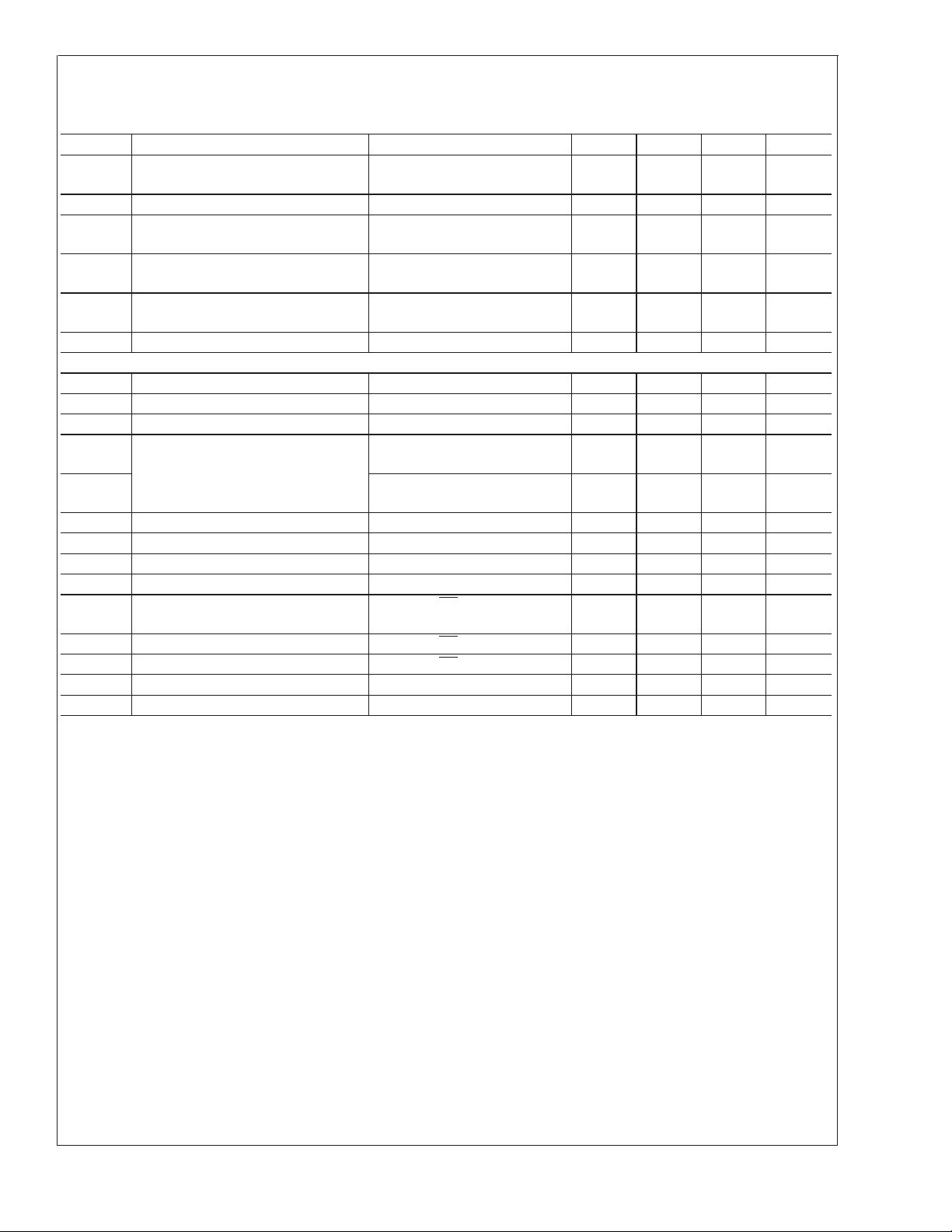
Electrical Characteristics (Continued)
Unless specified, AV= +2, RF= 300Ω:VCC=±5V, RL= 100Ω, LMH6714/6720/6722. Boldface limits apply at temperature
extremes.
Symbol Parameter Conditions Min Typ Max Units
I
BI
Input Bias Current Inverting −4
±
12
±
20
DIBI Average Drift 41 nA/˚C
PSRR Power Supply Rejection Ratio DC 48
58 dB
47
CMRR Common Mode Rejection Ratio DC 48
54 dB
45
I
CC
I
CCI
Supply Current RL=
Supply Current During Shutdown LMH6720 500 670 µA
∞
4.5
3
5.6 7.5
8
Miscellaneous Performance
R
IN
C
IN
R
OUT
V
O
V
OL
CMIR Input Voltage Range Common Mode
I
O
Input Resistance Non-Inverting 2 MΩ
Input Capacitance Non-Inverting 1.0 pF
Output Resistance Closed Loop 0.06 Ω
Output Voltage Range RL=
RL= 100Ω
∞
±
3.5
±
3.4
±
3.6
±
3.4
±
3.9 V
±
3.8 V
±
2.2 V
Output Current (Note 3) VIN= 0V, Max Linear Current 50 70 mA
OFFMAX Voltage for Shutdown LMH6720 0.8 V
ONMIN Voltage for Turn On LMH6720 2.0 V
IIH Current Turn On LMH6720, SD = 2.0V
−20
22030µA
−30
IIL Current Shutdown LMH6720, SD = .8V −600 −400 −100 µA
IOZ R
t
on
t
off
Note 1: Absolute Maximum Ratings indicate limits beyond which damage to the device may occur. Operating Ratings indicate conditions for which the device is
intended to be functional, but specific performance is not guaranteed. For guaranteed specifications, see the Electrical Characteristics tables.
Note 2: Electrical Table values apply only for factory testing conditions at the temperature indicated. Factory testing conditions result in very limited self-heating of
the device such that T
See Applications Section for information on temperature derating of this device." Min/Max ratings are based on product characterization and simulation. Individual
parameters are tested as noted.
Note 3: The maximum output current (I
more details.
Note 4: Human body model, 1.5kΩ in series with 100pF. Machine model, 0Ω In series with 200pF.
Note 5: The shutdown pin is designed to work between 0 and V
not be taken below V
Shutdown LMH6720, SD = .8V 0.2 1.8 MΩ
OUT
Turn on Time LMH6720 11 ns
Turn off Time LMH6720 7 ns
. No guarantee of parametric performance is indicated in the electrical tables under conditions of internal self heating where T
J=TA
) is determined by device power dissipation limitations. See the Power Dissipation section of the Application Division for
OUT
with split supplies (VCC=-VEE). With single supplies (VEE= ground) the shutdown pin should
/2.
CC
CC
µA
mA
>
TA.
J
LMH6714/6720/6722
www.national.com3
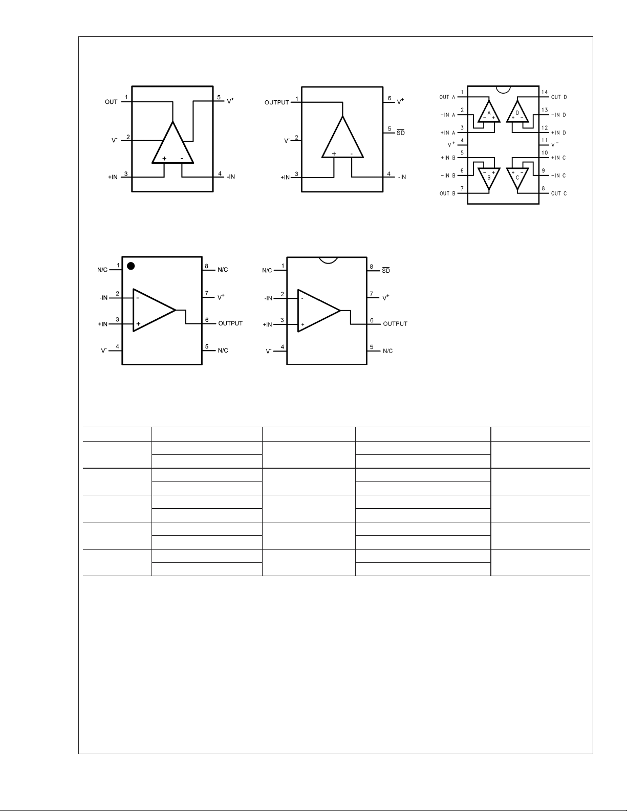
Connection Diagrams
5-Pin SOT23 (LMH6714) 6-Pin SOT23 (LMH6720) 14-Pin SOIC (LMH6722)
LMH6714/6720/6722
Top View
20056531
Top View
20056532
20056534
Top View
8-Pin SOIC (LMH6714) 8-Pin SOIC (LMH6720)
Top View
20056539
Top View
20056538
Ordering Information
Package Part Number Package Marking Transport Media NSC Drawing
5-Pin SOT23
8-Pin SOIC
6-Pin SOT23
8-Pin SOIC
14-Pin SOIC
LMH6714MF
LMH6714MFX 3k Units Tape and Reel
LMH6714MA
LMH6714MAX 2.5k Units Tape and Reel
LMH6720MF
LMH6720MFX 3k Units Tape and Reel
LMH6720MA
LMH6720MAX 2.5k Units Tape and Reel
LMH6722MA
LMH6722MAX 2.5 Units Tape and Reel
A95A
LMH6714MA
A96A
LMH6720MA
LMH6722MA
1k Units Tape and Reel
95 Units/Rail
1k Units Tape and Reel
95 Units/Rail
55 Units/Rail
MF05A
M08A
MF06A
M08A
M14A
www.national.com 4
LMH6714/6720/6722
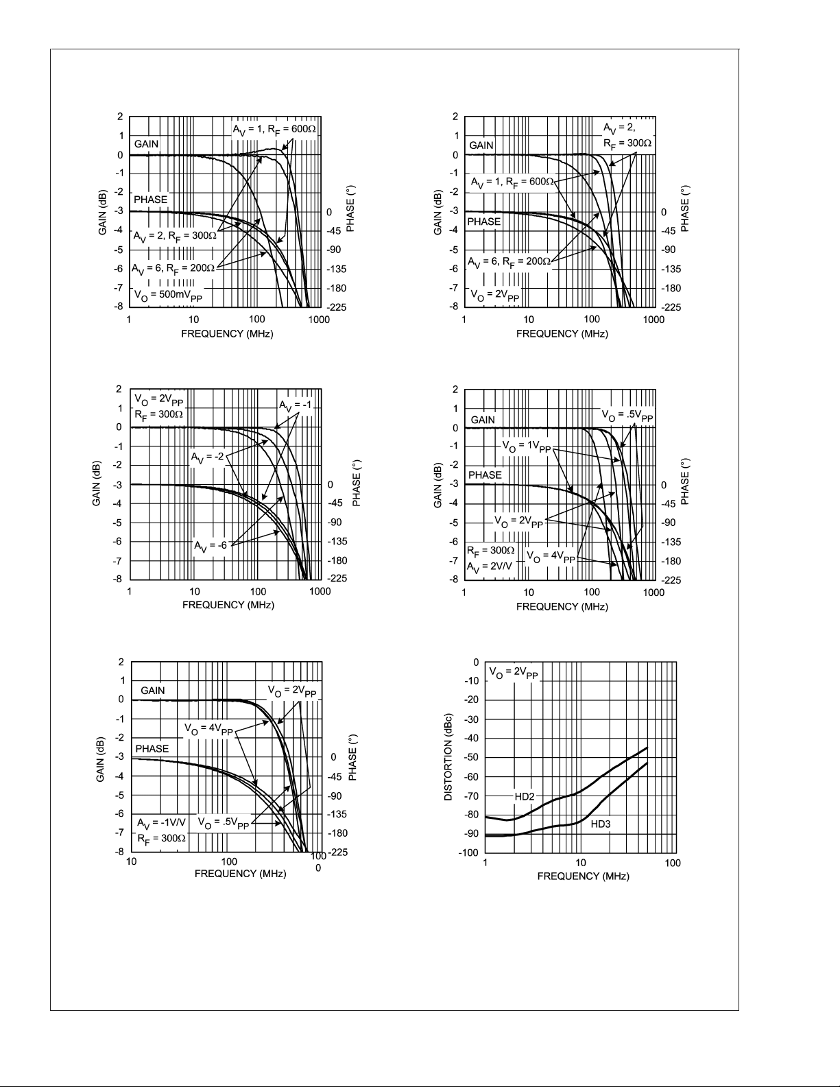
Typical Performance Characteristics (A
=2,RF= 300Ω,RL= 100Ω Unless Specified).
V
Non-Inverting Small Signal Frequency Response Non-Inverting Large Signal Frequency Response
20056506 20056507
Inverting Frequency Response Non-Inverting Frequency Response vs. V
O
Inverting Frequency Response vs. V
O
20056509
20056503
20056508
Harmonic Distortion vs. Frequency
20056504
www.national.com5

Typical Performance Characteristics (A
Specified). (Continued)
=2,RF= 300Ω,RL= 100Ω Unless
V
2nd Harmonic Distortion vs. V
LMH6714/6720/6722
OUT
20056502
3rd Harmonic Distortion vs. V
DG/DP (LMH6714) DG/DP (LMH6720)
OUT
20056501
20056528
DG/DP (LMH6722) Large Signal Pulse Response
20056535
www.national.com 6
20056505
20056513

LMH6714/6720/6722
Typical Performance Characteristics (A
Specified). (Continued)
Small Signal Pulse Response Closed Loop Output Resistance
20056510
Open Loop Transimpedance Z(s) PSRR vs. Frequency
=2,RF= 300Ω,RL= 100Ω Unless
V
20056511
20056523
CMRR vs. Frequency Frequency Response vs. R
20056525
20056516
F
20056512
www.national.com7

Typical Performance Characteristics (A
Specified). (Continued)
=2,RF= 300Ω,RL= 100Ω Unless
V
DC Errors vs. Temperature Maximum V
LMH6714/6720/6722
3rd Order Intermodulation vs. Output Power
vs. Frequency
OUT
20056518 20056526
Crosstalk vs. Frequency (LMH6722)
for each channel with all others active
20056527 20056536
www.national.com 8

Application Section
FEEDBACK RESISTOR SELECTION
One of the key benefits of a current feedback operational
amplifier is the ability to maintain optimum frequency response independent of gain by using appropriate values for
the feedback resistor (R
Typical Performance plots specify an R
±
+2V/V and
5V power supplies (unless otherwise specified).
Generally, lowering R
peak the frequency response and extend the bandwidth
while increasing the value of R
response to roll off faster. Reducing the value of R
below it’s recommended value will cause overshoot, ringing
and, eventually, oscillation.
). The Electrical Characteristics and
F
from it’s recommended value will
F
F
of 300Ω, a gain of
F
will cause the frequency
F
too far
LMH6714/6720/6722
20056515
FIGURE 2. RFvs. Non-Inverting Gain
20056512
FIGURE 1. Frequency Response vs. R
The plot labeled "Frequency Response vs. R
LMH6714/6720/6722’s frequency response as R
= 100Ω,AV= +2). This plot shows that an RFof 147Ω
(R
L
results in peaking. An R
of 300Ω gives near maximal band-
F
width and gain flatness with good stability. An R
F
" shows the
F
is varied
F
of 400Ω
F
gives excellent stability with only a small bandwidth penalty.
Since all applications are slightly different it is worth some
experimentation to find the optimal R
for a given circuit.
F
Note that it is not possible to use a current feedback amplifier
with the output shorted directly to the inverting input. The
buffer configuration of the LMH6714/6720/6722 requires a
600Ω feedback resistor for stable operation.
For more information see Application Note OA-13 which
describes the relationship between R
and closed-loop fre-
F
quency response for current feedback operational amplifiers.
The value for the inverting input impedance for the
LMH6714/6720/6722 is approximately 180Ω. The LMH6714/
6720/6722 is designed for optimum performance at gains of
±
+1 to +6 V/V and −1 to −5V/V. When using gains of
more the low values of R
required will make inverting input
G
7V/V or
impedances very low.
When configuring the LMH6714/6720/6722 for gains other
than +2V/V, it is usually necessary to adjust the value of the
feedback resistor. The two plots labeled “R
inverting Gain” and “R
vs. Inverting Gain” provide recom-
F
vs. Non-
F
mended feedback resistor values for a number of gain selections.
In the “R
Gain” charts the recommended value of R
vs. Non-Inverting Gain” and the “RFvs. Inverting
F
is depicted by
F
the solid line, which starts high, decreases to 200Ω and
begins increasing again. The reason that a higher R
required at higher gains is the need to keep R
from de-
G
F
creasing too far below the output impedance of the input
buffer. For the LMH6714/6720/6722 the output resistance of
the input buffer is approximately 180Ω and 50Ω is a practical
lower limit for R
. Due to the limitations on RGthe LMH6714/
G
6720/6722 begins to operate in a gain bandwidth limited
±
fashion for gains of
5V/V or greater.
20056514
FIGURE 3. RFvs. Inverting Gain
ACTIVE FILTERS
When using any current feedback Operational Amplifier as
an active filter it is important to be very careful when using
reactive components in the feedback loop. Anything that
reduces the impedance of the negative feedback, especially
at higher frequencies, will almost certainly cause stability
problems. Likewise capacitance on the inverting input needs
is
www.national.com9

Application Section (Continued)
to be avoided. See Application Notes OA-7 and OA-26 for
more information on Active Filter applications for Current
Feedback Op Amps.
LMH6714/6720/6722
20056524
20056521
FIGURE 4. Enable/Disable Operation
±
ENABLE/DISABLE OPERATION USING
5V SUPPLIES
(LMH6720 ONLY)
The LMH6720 has a TTL logic compatible disable function.
<
Apply a logic low (
disabled. Apply a logic high (
.8V) to the DS pin and the LMH6720 is
>
2.0V), or let the pin float and
the LMH6720 is enabled. Voltage, not current, at the Disable
pin determines the enable/disable state. Care must be exercised to prevent the disable pin voltage from going more
than .8V below the midpoint of the supply voltages (0V with
split supplies, V
/2 with single supplies) doing so could
CC
cause transistor Q1 to Zener resulting in damage to the
disable circuit. The core amplifier is unaffected by this, but
disable operation could become slower as a result.
Disabled, the LMH6720 inputs and output become high impedances. While disabled the LMH6720 quiescent current is
approximately 500µA. Because of the pull up resistor on the
disable circuit the I
the disabled state. The positive supply current (I
proximately 500µA while the negative supply current (I
only 200µA. The remaining I
and IEEcurrents are not balanced in
CC
CC
current of 300µA flows
EE
)isap-
)is
EE
through the disable pin.
The disable function can be used to create analog switches
or multiplexers. Implement a single analog switch with one
LMH6720 positioned between an input and output. Create
an analog multiplexer with several LMH6720’s. The
LMH6720 is at it’s best at a gain of 1 for multiplexer applications because there is no R
to shunt signals to ground.
G
DISABLE LIMITATIONS (LMH6720 ONLY)
The feedback Resistor (R
) limits off isolation in inverting
F
gain configurations. During shutdown the impedance of the
>
LMH6720 inputs and output become very high (
however R
and RGare the dominant factor for effective
F
1MΩ),
output impedance.
Do not apply voltages greater than +V
/2 single supply) to the disable pin. The input ESD
(V
CC
or less than 0V
CC
diodes will also conduct if the signal leakage through the
feedback resistors brings the inverting input near either supply rail.
FIGURE 5. Typical Application with Suggested Supply
Bypassing
LAYOUT CONSIDERATIONS
Whenever questions about layout arise, use the evaluation
board as a guide. The following Evaluation boards are available with sample parts:
LMH6714 SOT CLC730216
SOIC CLC730227
LMH6720 SOT CLC730216
SOIC CLC730227
LMH6722 SOIC CLC730231
To reduce parasitic capacitances, the ground plane should
be removed near the input and output pins. To reduce series
inductance, trace lengths of components in the feedback
loop should be minimized. For long signal paths controlled
impedance lines should be used, along with impedance
matching at both ends.
Bypass capacitors should be placed as close to the device
as possible. Bypass capacitors from each rail to ground are
applied in pairs. The larger electrolytic bypass capacitors
can be located anywhere on the board, the smaller ceramic
capacitors should be placed as close to the device as possible. In addition Figure 2 shows a capacitor (C1) across the
supplies with no connection to ground. This capacitor is
optional, however it is required for best 2nd Harmonic suppression. If this capacitor is omitted C2 and C3 should be
increased to .1µF each.
VIDEO PERFORMANCE
The LMH6714/6720/6722 has been designed to provide excellent performance with both PAL and NTSC composite
video signals. Performance degrades as the loading is increased, therefore best performance will be obtained with
back terminated loads. The back termination reduces reflections from the transmission line and effectively masks capacitance from the amplifier output stage. While all parts
offer excellent video performance the LMH6714 and
LMH6722 are slightly better than the LMH6720.
www.national.com 10

Application Section (Continued)
WIDE BAND DIGITAL PROGRAMMABLE GAIN AMPLIFIER (LMH6720 ONLY)
LMH6714/6720/6722
20056519
FIGURE 6. Wideband Digitally Controlled Programmable Gain Amplifier
Channel Switching
FIGURE 7. PGA Output
As shown in Figure 6 and Figure 7 the LMH6720 can be
used to construct a digitally controlled programmable gain
amplifier. Each amplifier is configured to provide a digitally
selectable gain. To provide for accurate gain settings, 1% or
better tolerance is recommended on the feedback and gain
resistors. The gain provided by each digital code is arbitrary
through selection of the feedback and gain resistor values.
AMPLITUDE EQUALIZATION
Sending signals over coaxial cable greater than 50 meters in
length will attenuate high frequency signal components
much more than lower frequency components. An equalizer
can be made to pre emphasize the higher frequency components so that the final signal has less distortion. This
process can be done at either end of the cable. The circuit in
Figure 8 shows a receiver with some additional components
20056520
in the feedback loop to equalize the incoming signal. The RC
networks peak the signal at higher frequencies. This peaking
is a piecewise linear approximation of the inverse of the
frequency response of the coaxial cable. Figure 9 shows the
effect of this equalization on a digital signal that has passed
through 150 meters of coaxial cable. Figure 10 shows a
Bode plot of the frequency response of the circuit in Figure 8
along with equations needed to design the pole and zero
frequencies. Figure 11 shows a network analyzer plot of an
LMH6714/6720/6722 with the following component values:
= 309Ω
R
G
R1 = 450Ω
C1 = 470pF
R2=91Ω
C2 = 68pF
www.national.com11

Application Section (Continued)
LMH6714/6720/6722
FIGURE 8.
20056522
20056529
20056517
FIGURE 11. Equalizer Frequency Response
POWER DISSIPATION
Follow these steps to determine the Maximum power dissipation for the LMH6714/6720/6722:
1. Calculate the quiescent (no load) power: P
AMP=ICC
(VCC-VEE)
2. Calculate the RMS power at the output stage:
(RMS) = ((VCC-V
P
OUT
where V
OUT
and I
are the voltage and current across
OUT
OUT
(RMS))*I
OUT
(RMS)),
the external load.
3. Calculate the total RMS power: P
T=PAMP+POUT
The maximum power that the LMH6714/6720/6722, package can dissipate at a given temperature can be derived with
the following equation:
= (150˚ - TA)/ θJA, where TA= Ambient temperature
P
MAX
(˚C) and θ
for a given package (˚C/W). For the SOIC package θ
= Thermal resistance, from junction to ambient,
JA
JA
148˚C/W, for the SOT it is 250˚C/W.
is
FIGURE 9. Digital Signal without and with Equalization
20056530
FIGURE 10. Design Equations
www.national.com 12

Physical Dimensions inches (millimeters)
unless otherwise noted
LMH6714/6720/6722
5-Pin SOT23
NS Product Number MF05A
6-Pin SOT23
NS Product Number MF06A
www.national.com13

Physical Dimensions inches (millimeters) unless otherwise noted (Continued)
LMH6714/6720/6722
8-Pin SOIC
NS Product Number M08A
14-Pin SOIC
NS Product Number M14A
www.national.com 14

Notes
LMH6714/6720/6722 Wideband Video Op Amp; Single, Single with Shutdown and Quad
LIFE SUPPORT POLICY
NATIONAL’S PRODUCTS ARE NOT AUTHORIZED FOR USE AS CRITICAL COMPONENTS IN LIFE SUPPORT
DEVICES OR SYSTEMS WITHOUT THE EXPRESS WRITTEN APPROVAL OF THE PRESIDENT AND GENERAL
COUNSEL OF NATIONAL SEMICONDUCTOR CORPORATION. As used herein:
1. Life support devices or systems are devices or
systems which, (a) are intended for surgical implant
into the body, or (b) support or sustain life, and
whose failure to perform when properly used in
accordance with instructions for use provided in the
2. A critical component is any component of a life
support device or system whose failure to perform
can be reasonably expected to cause the failure of
the life support device or system, or to affect its
safety or effectiveness.
labeling, can be reasonably expected to result in a
significant injury to the user.
National Semiconductor
Americas Customer
Support Center
Email: new.feedback@nsc.com
Tel: 1-800-272-9959
www.national.com
National does not assume any responsibility for use of any circuitry described, no circuit patent licenses are implied and National reserves the right at any time without notice to change said circuitry and specifications.
National Semiconductor
Europe Customer Support Center
Fax: +49 (0) 180-530 85 86
Email: europe.support@nsc.com
Deutsch Tel: +49 (0) 69 9508 6208
English Tel: +44 (0) 870 24 0 2171
Français Tel: +33 (0) 1 41 91 8790
National Semiconductor
Asia Pacific Customer
Support Center
Fax: +65-6250 4466
Email: ap.support@nsc.com
Tel: +65-6254 4466
National Semiconductor
Japan Customer Support Center
Fax: 81-3-5639-7507
Email: jpn.feedback@nsc.com
Tel: 81-3-5639-7560
 Loading...