

查询LMH6639供应商
LMH6639
190MHz Rail-to-Rail Output Amplifier with Disable
LMH6639 190MHz Rail-to-Rail Output Amplifier with Disable
July 2003
General Description
The LMH6639 is a voltage feedback operational amplifier
with a rail-to-rail output drive capability of 110mA. Employing
National’s patented VIP10 process, the LMH6639 delivers a
bandwidth of 190MHz at a current consumption of only
3.6mA. An input common mode voltage range extending to
0.2V below the V
LMH6639 a true single supply op-amp. The output voltage
range extends to within 30mV of either supply rail providing
the user with a dynamic range that is especially desirable in
low voltage applications.
The LMH6639 offers a slew rate of 172V/µs resulting in a full
power bandwidth of approximately 28MHz. The T
83nsec combined with a settling time of 33nsec makes this
device ideally suited for multiplexing applications. Careful
attention has been paid to ensure device stability under all
operating voltages and modes. The result is a very well
behaved frequency response characteristic for any gain setting including +1, and excellent specifications for driving
video cables including harmonic distortion of −60dBc, differential gain of 0.12% and differential phase of 0.045˚
−
and to within 1V of V+, makes the
value of
ON
Features
(VS= 5V, Typical values unless specified)
n Supply current (no load) 3.6mA
n Supply current (off mode) 400µA
n Output resistance (closed loop 1MHz) 0.186Ω
n −3dB BW (A
n Settling time 33nsec
n Input common mode voltage −0.2V to 4V
n Output voltage swing 40mV from rails
n Linear output current 110mA
n Total harmonic distortion −60dBc
n Fully characterized for 3V, 5V and
n No output phase reversal with CMVR exceeded
n Excellent overdrive recovery
n Off Isolation 1MHz −70dB
n Differential Gain 0.12%
n Differential Phase 0.045˚
= 1) 190MHz
V
±
5V
Applications
n Active filters
n CD/DVD ROM
n ADC buffer amplifier
n Portable video
n Current sense buffer
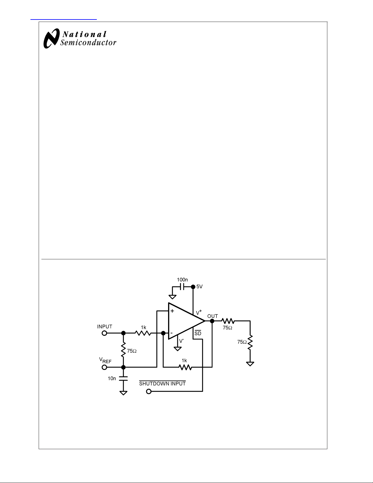
20030246
FIGURE 1. Typical Single Supply Schematic
© 2003 National Semiconductor Corporation DS200302 www.national.com
Absolute Maximum Ratings (Note 1)
If Military/Aerospace specified devices are required,
please contact the National Semiconductor Sales Office/
LMH6639
Distributors for availability and specifications.
Junction Temperature (Note 4) +150˚C
Soldering Information
Infrared or Convection (20 sec) 235˚C
Wave Soldering (10 sec) 260˚C
ESD Tolerance 2KV (Note 2)
200V (Note 9)
Differential
V
IN
Input Current
Supply Voltage (V
+–V−
) 13.5V
Voltage at Input/Output pins V
+
+0.8V, V−−0.8V
±
±
10mA
2.5V
Storage Temperature Range −65˚C to +150˚C
Operating Ratings (Note 1)
Operating Temperature Range (Note 4) −40˚C to +85˚C
Package Thermal Resistance (θ
SOT23-6 265˚C/W
SOIC-8 190˚C/W
) (Note 4)
JA
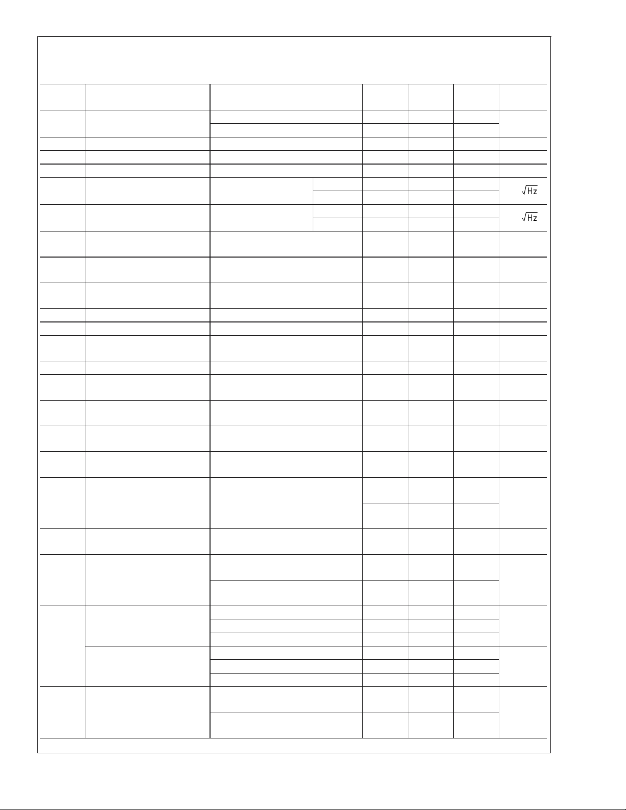
3V Electrical Characteristics
Unless otherwise specified, all limits guaranteed for at TJ= 25˚C, V+= 3V, V−= 0V, VO=VCM=V+/2, and RL=2kΩ to V+/2.
Boldface limits apply at the temperature extremes.
Symbol Parameter Conditions Min
(Note 6)
BW −3dB BW A
BW
0.1dB
0.1dB Gain Flatness RF= 2.65kΩ ,RL=1kΩ, 16.4 MHz
FPBW Full Power Bandwidth A
GBW Gain Bandwidth product A
e
n
Input-Referred Voltage Noise RF= 33kΩ f = 10kHz 19
= +1 120 170
V
A
=−1 63
V
= +1, V
V
+
= 1.8V, V−= 1.2V
V
= +1 83 MHz
V
=2VPP, −1dB
OUT
f = 1MHz 16
i
n
Input-Referred Current Noise RF=1MΩ f = 10kHz 1.30
f = 1MHz 0.36
THD Total Harmonic Distortion f = 5MHz, V
=1kΩ to V+/2
R
L
T
S
SR Slew Rate A
V
OS
TC V
I
B
I
OS
R
IN
Settling Time VO=2VPP,±0.1% 37 ns
= −1 (Note 8) 120 167 V/µs
V
Input Offset Voltage 1.01 5
Input Offset Average Drift (Note 11) 8 µV/˚C
OS
Input Bias Current (Note 7) −1.02 −2.6
Input Offset Current 20 800
Common Mode Input
AV= +1, f = 1kHz, RS=1MΩ 6.1 MΩ
=2VPP,AV= +2,
O
Resistance
C
IN
Common Mode Input
AV= +1, RS= 100kΩ 1.35 pF
Capacitance
CMVR Input Common-Mode Voltage
CMRR ≥ 50dB −0.3 −0.2
Range
CMRR Common Mode Rejection
(Note 12) 72 93 dB
Ratio
A
VOL
Large Signal Voltage Gain VO=2VPP,RL=2kΩ to V+/2 80
=2VPP,RL= 150Ω to V+/2 74
V
O
1.8
1.6
76
70
Typ
(Note 5)
Max
(Note 6)
21 MHz
−50
7
−3.5
1000
−0.1
2
100
78
Units
MHz
nV/
pA/
dBc
mV
µA
nA
V
dB
www.national.com 2
3V Electrical Characteristics (Continued)
Unless otherwise specified, all limits guaranteed for at TJ= 25˚C, V+= 3V, V−= 0V, VO=VCM=V+/2, and RL=2kΩ to V+/2.
Boldface limits apply at the temperature extremes.
Symbol Parameter Conditions Min
(Note 6)
V
O
Output Swing
High
Output Swing
Low
I
SC
Output Short Circuit Current Sourcing to V+/2, (Note 10) 50
RL=2kΩ to V+/2, VID= 200mV 2.90 2.98
= 150Ω to V+/2, VID= 200mV 2.75 2.93
L
R
=50Ω to V+/2, VID= 200mV 2.6 2.85
L
R
=2kΩ to V+/2, VID= −200mV 25 75
L
= 150Ω to V+/2, VID= −200mV 75 200
L
R
=50Ω to V+/2, VID= −200mV 130 300
L
35
+
Sinking to V
/2, (Note 10) 67
40
I
OUT
Output Current VO= 0.5V from either supply 99 mA
PSRR Power Supply Rejection Ratio (Note 12) 72 96 dB
I
S
Supply Current (Enabled) No Load 3.5 5.6
Supply Current (Disabled) 0.3 0.5
TH_SD Threshold Voltage for
Shutdown Mode
I_SD PIN Shutdown Pin Input Current SD Pin Connect to 0V (Note 7) −13 µA
T
ON
T
OFF
R
OUT
On Time After Shutdown 83 nsec
Off Time to Shutdown 160 nsec
Output Resistance Closed
Loop
RF= 10kΩ, f = 1kHz, AV=−1 27
R
= 10kΩ, f = 1MHz, AV= −1 266
F
Typ
(Note 5)
Max
(Note 6)
120
140
7.5
0.7
+
−1.59 V
V
Units
mVR
mA
mA
mΩ
LMH6639
VR
5V Electrical Characteristics
Unless otherwise specified, all limits guaranteed for at TJ= 25˚C, V+= 5V, V−= 0V, VO=VCM=V+/2, and RL=2kΩ to V+/2.
Boldface limits apply at the temperature extremes.
Symbol Parameter Conditions Min
(Note 6)
BW −3dB BW A
BW
0.1dB
0.1dB Gain Flatness RF= 2.51kΩ,RL=1kΩ, 16.4 MHz
FPBW Full Power Bandwidth A
GBW Gain Bandwidth Product A
e
n
Input-Referred Voltage Noise RF= 33kΩ f = 10kHz 19
= +1 130 190
V
A
=−1 64
V
= +1, V
V
= +1 86 MHz
V
=2VPP, −1dB 28 MHz
OUT
f = 1MHz 16
i
n
Input-Referred Current Noise RF=1MΩ f = 10KHz 1.35
f = 1MHz 0.35
THD Total Harmonic Distortion f = 5MHz, V
=1kΩ to V+/2
R
L
DG Differential Gain NTSC, A
= 150Ω to V+/2
R
L
DP Differential Phase NTSC, A
= 150Ω to V+/2
R
L
T
S
SR Slew Rate A
V
OS
Settling Time VO=2VPP,±0.1% 33 ns
= −1, (Note 8) 130 172 V/µs
V
Input Offset Voltage 1.02 5
=2VPP,AV=+2
O
=+2
V
=+2
V
Typ
(Note 5)
Max
(Note 6)
nV/
pA/
−60 dBc
0.12 %
0.045 deg
7
Units
MHz
mV
www.national.com3
5V Electrical Characteristics (Continued)
Unless otherwise specified, all limits guaranteed for at TJ= 25˚C, V+= 5V, V−= 0V, VO=VCM=V+/2, and RL=2kΩ to V+/2.
Boldface limits apply at the temperature extremes.
LMH6639
Symbol Parameter Conditions Min
(Note 6)
TC V
I
B
I
OS
R
IN
Input Offset Average Drift (Note 11) 8 µV/˚C
OS
Input Bias Current (Note 7) −1.2 −2.6
Input Offset Current 20 800
Common Mode Input
AV= +1, f = 1kHz, RS=1MΩ 6.88 MΩ
Resistance
C
IN
Common Mode Input
AV= +1, RS= 100kΩ 1.32 pF
Capacitance
CMVR Common-Mode Input Voltage
CMRR ≥ 50dB −0.3 −0.2
Range
CMRR Common Mode Rejection
(Note 12) 72 95 dB
Ratio
A
VOL
Large Signal Voltage Gain VO=4V
PP
RL=2kΩ to V+/2
V
= 3.75V
O
PP
RL= 150Ω to V+/2
V
O
I
SC
Output Swing
High
Output Swing
Low
RL=2kΩ to V+/2, VID= 200mV 4.90 4.97
= 150Ω to V+/2, VID= 200mV 4.65 4.90
L
R
=50Ω to V+/2, VID= 200mV 4.40 4.77
L
R
=2kΩ to V+/2, VID= −200mV 25 100
L
= 150Ω to V+/2, VID= −200mV 85 200
L
R
=50Ω to V+/2, VID= −200mV 190 400
L
Output Short Circuit Current Sourcing to V+/2, (Note 10) 100
86
82
74
70
79
+
Sinking from V
/2, (Note 10) 120
85
I
OUT
Output Current VO= 0.5V from either supply 110 mA
PSRR Power Supply Rejection Ratio (Note 12) 72 96 dB
I
S
Supply Current (Enabled) No Load 3.6 5.8
Supply Current (Disabled) 0.40 0.8
TH_SD Threshold Voltage for
Shutdown Mode
I_SD PIN Shutdown Pin Input Current SD Pin Connected to 0V (Note 7) −30 µA
T
ON
T
OFF
R
OUT
On Time after Shutdown 83 nsec
Off Time to Shutdown 160 nsec
Output Resistance Closed
Loop
RF= 10kΩ, f = 1kHz, AV=−1 29
R
= 10kΩ, f = 1MHz, AV= −1 253
F
Typ
(Note 5)
Max
(Note 6)
−3.25
1000
−0.1
4 3.8
3.6
100
77
160
190
8.0
1.0
V+−1.65 V
Units
µA
nA
V
dB
VR
mVR
mA
mA
mΩ
www.national.com 4
±
5V Electrical Characteristics
Unless otherwise specified, all limits guaranteed for at TJ= 25˚C, V
=±5V, VO=VCM= GND, and RL=2kΩ to V+/2.
SUPPLY
Boldface limits apply at the temperature extremes.
Symbol Parameter Conditions Min
(Note 6)
BW −3dB BW A
BW
0.1dB
0.1dB Gain Flatness RF= 2.26kΩ,RL=1kΩ 18 MHz
FPBW Full Power Bandwidth A
GBW Gain Bandwidth Product A
e
n
Input-Referred Voltage Noise RF= 33kΩ f = 10kHz 19
= +1 150 228
V
A
=−1 65
V
= +1, V
V
= +1 90 MHz
V
=2VPP, −1dB 29 MHz
OUT
f = 1MHz 16
i
n
Input-Referred Current Noise RF=1MΩ f = 10kHz 1.13
f = 1MHz 0.34
THD Total Harmonic Distortion f = 5MHz, V
=1kΩ
R
L
DG Differential Gain NTSC, A
= 150Ω
R
L
DP Differential Phase NTSC, A
= 150Ω
R
L
T
S
SR Slew Rate A
V
OS
TC V
I
B
I
OS
R
IN
Settling Time VO=2VPP,±0.1% 33 ns
= −1 (Note 8) 140 200 V/µs
V
Input Offset Voltage 1.03 5
Input Offset Voltage Drift (Note 11) 8 µV/˚C
OS
Input Bias Current (Note 7) −1.40 −2.6
Input Offset Current 20 800
Common Mode Input
AV+1, f = 1kHz, RS=1MΩ 7.5 MΩ
=2VPP,AV= +2,
O
=+2
V
=+2
V
Resistance
C
IN
Common Mode Input
AV= +1, RS= 100kΩ 1.28 pF
Capacitance
CMVR Common Mode Input Voltage
CMRR ≥ 50dB −5.3 −5.2
Range
CMRR Common Mode Rejection
(Note 12) 72 95 dB
Ratio
A
VOL
Large Signal Voltage Gain VO=9VPP,RL=2kΩ 88
VO=8VPP,RL= 150Ω 74
V
O
Output Swing
High
Output Swing
Low
I
SC
Output Short Circuit Current Sourcing to Ground, (Note 10) 100
RL=2kΩ,VID= 200mV 4.85 4.96
= 150Ω,VID= 200mV 4.55 4.80
L
R
=50Ω,VID= 200mV 3.60 4.55
L
R
=2kΩ,VID= −200mV −4.97 −4.90
L
= 150Ω,VID= −200mV −4.85 −4.55
L
R
=50Ω,VID= −200mV −4.65 −4.30
L
Sinking to Ground, (Note 10) 110
3.8
3.6
84
70
80
85
Typ
(Note 5)
Max
(Note 6)
nV/
pA/
−71.2 dBc
0.11 %
0.053 deg
7
−3.25
1000
−5.1
4.0
100
77
168
190
LMH6639
Units
MHz
mV
µA
nA
V
dB
VR
VR
mA
www.national.com5
±
5V Electrical Characteristics (Continued)
Unless otherwise specified, all limits guaranteed for at TJ= 25˚C, V
Boldface limits apply at the temperature extremes.
LMH6639
Symbol Parameter Conditions Min
I
OUT
Output Current VO= 0.5V from either supply 112 mA
=±5V, VO=VCM= GND, and RL=2kΩ to V+/2.
SUPPLY
Typ
(Note 6)
(Note 5)
(Note 6)
Max
PSRR Power Supply Rejection Ratio (Note 12) 72 96 dB
I
S
Supply Current (Enabled) No Load 4.18 6.5
8.5
Supply Current (Disabled) 0.758 1.0
1.3
+
TH_SD Threshold Voltage for
− 1.67 V
V
Shutdown Mode
I_SD PIN Shutdown Pin Input Current SD Pin Connected to −5V (Note 7) −84 µA
T
ON
T
OFF
R
OUT
Note 1: Absolute Maximum Ratings indicate limits beyond which damage to the device may occur. Operating Ratings indicate conditions for which the device is
intended to be functional, but specific performance is not guaranteed. For guaranteed specifications and the test conditions, see the Electrical Characteristics.
Note 2: Human body model, 1.5kΩ in series with 100pF.
Note 3: Applies to both single-supply and split-supply operation. Continuous short circuit operation at elevated ambient temperature can result in exceeding the
maximum allowed junction temperature of 150˚C.
Note 4: The maximum power dissipation is a function of T
P
D
Note 5: Typical values represent the most likely parametric norm.
Note 6: All limits are guaranteed by testing or statistical analysis.
Note 7: Positive current corresponds to current flowing into the device.
Note 8: Slew rate is the average of the rising and falling slew rates.
Note 9: Machine Model, 0Ω in series with 200pF.
Note 10: Short circuit test is a momentary test.
Note 11: Offset voltage average drift determined by dividing the change in V
Note 12: f ≤ 1kHz (see typical performance Characteristics)
On Time after Shutdown 83 nsec
Off Time to Shutdown 160 nsec
Output Resistance Closed
Loop
=(T
J(MAX)-TA
)/ θJA. All numbers apply for packages soldered directly onto a PC board.
RF= 10kΩ, f = 1kHz, AV=−1 32
R
= 10kΩ, f = 1MHz, AV= −1 226
F
, θJA, and TA. The maximum allowable power dissipation at any ambient temperature is
J(MAX)
at temperature extremes into the total temperature change.
OS
Units
mA
mΩ
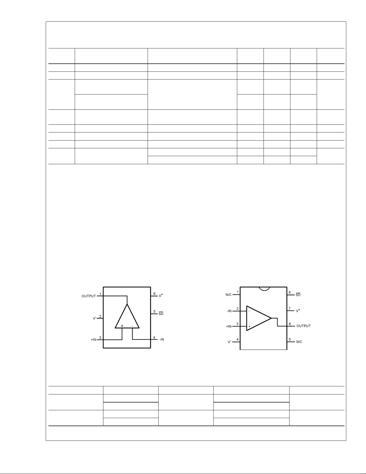
Connection Diagrams
SOT23-6 SOIC-8
Top View
20030201
Top View
20030202
Ordering Information
Package Part Number Package Marking Transport Media NSC Drawing
6-Pin SOT-23 LMH6639MF A81A 1k Units Tape and Reel MF06A
LMH6639MFX 3k Units Tape and Reel
8-Pin SOIC LMH6639MA LMH6639MA Rails M08A
LMH6639MAX 2.5k Units Tape and Reel
www.national.com 6

LMH6639
Typical Performance Characteristics At T
=1kΩ for AV= −1. Unless otherwise specified.
R
F
Output Sinking Saturation Voltage vs. I
for Various Temperature
Positive Output Saturation Voltage vs. V
for Various Temperature
OUT
20030239
SUPPLY
= 25˚C, V+= +2.5, V−= −2.5V, RF= 330Ω for AV= +2,
J
Output Sourcing Saturation Voltage vs. I
OUT
for Various Temperature
20030237
Negative Output Saturation Voltage vs. V
SUPPLY
for Various Temperature
V
OUT
from V+vs. I
SOURCE
20030233
V
from V−vs. I
OUT
20030238 20030236
SINK
20030234
www.national.com7

Typical Performance Characteristics At T
=1kΩ for AV= −1. Unless otherwise specified. (Continued)
R
F
LMH6639
I
vs. VSfor Various Temperature VOSvs. VSfor 3 Representative Units
OS
20030232 20030245
VOSvs. VSfor 3 Representative Units VOSvs. VSfor 3 Representative Units
= 25˚C, V+= +2.5, V−= −2.5V, RF= 330Ω for AV= +2,
J
20030244
VOSvs. VSfor 3 Representative Units I
20030242 20030240
www.national.com 8
vs. VCMfor Various Temperature
SUPPLY
20030243

LMH6639
Typical Performance Characteristics At T
=1kΩ for AV= −1. Unless otherwise specified. (Continued)
R
F
I
vs. VSfor Various Temperature IBvs. VSfor Various Temperature
SUPPLY
20030241 20030235
Bandwidth for Various V
S
= 25˚C, V+= +2.5, V−= −2.5V, RF= 330Ω for AV= +2,
J
Bandwidth for Various V
S
20030206 20030205
Gain vs. Frequency Normalized Gain vs. Frequency Normalized
20030207 20030208
www.national.com9

Typical Performance Characteristics At T
=1kΩ for AV= −1. Unless otherwise specified. (Continued)
R
F
LMH6639
0.1dB Gain Flatness
20030209 20030204
Frequency Response vs. Temperature Harmonic Distortion
= 25˚C, V+= +2.5, V−= −2.5V, RF= 330Ω for AV= +2,
J
Gain and phase vs.
Frequency for Various Temperature
20030210
Differential Gain/Phase On-Off Switching DC Voltage
20030270
www.national.com 10
20030269
20030211

LMH6639
Typical Performance Characteristics At T
=1kΩ for AV= −1. Unless otherwise specified. (Continued)
R
F
On-Off Switching 10MHz Slew Rate (Positive)
20030212
Slew Rate (Negative) On-Off Switching of Sinewave
= 25˚C, V+= +2.5, V−= −2.5V, RF= 330Ω for AV= +2,
J
20030214
20030213 20030215
Power Sweep CMRR vs. Frequency
20030216 20030218
www.national.com11

Typical Performance Characteristics At T
=1kΩ for AV= −1. Unless otherwise specified. (Continued)
R
F
LMH6639
PSRR vs. Frequency Current Noise
20030217 20030220
Voltage Noise Closed Loop Output Resistance vs. Frequency
= 25˚C, V+= +2.5, V−= −2.5V, RF= 330Ω for AV= +2,
J
20030219
Off Isolation Small Signal Pulse Response (AV= +1, RL=2k)
20030222
www.national.com 12
20030221
20030250

LMH6639
Typical Performance Characteristics At T
=1kΩ for AV= −1. Unless otherwise specified. (Continued)
R
F
Small Signal Pulse Response (A
Large Signal Pulse Response Large Signal Pulse Response
= −1) Large Signal Pulse Response (RL= 2k)
V
20030249
= 25˚C, V+= +2.5, V−= −2.5V, RF= 330Ω for AV= +2,
J
20030226
20030227 20030228
www.national.com13

Application Notes
MULTIPLEXING 5 AND 10MHz
LMH6639
The LMH6639 may be used to implement a circuit which
multiplexes two signals of different frequencies. Three
LMH6639 high speed op-amps are used in the circuit of
Figure 2 to accomplish the multiplexing function. Two
LMH6639 are used to provide gain for the input signals, and
the third device is used to provide output gain for the selected signal.
In the circuit of Figure 2, the outputs of IC1 and IC2 are tied
together such that their output impedances are placed in
parallel at the input of IC3. The output impedance of the
disabled amplifier is high compared both to the output impedance of the active amplifier and the 330Ω gain setting
resistors. The closed loop output resistance for the
LMH6639 is around 0.2Ω. Thus the active state amplifier
output impedance dominates the input node to IC3, while the
disabled amplifier is assured of a high level of suppression of
unwanted signals which might be present at the output.
SHUTDOWN OPERATION
With SD pin left floating, the device enters normal operation.
However, since the SD pin has high input impedance, it is
best tied to V+for normal operation. This will avoid inadvertent shutdown due to capacitive pick-up from nearby nodes.
LMH6639 will typically go into shutdown when SD pin is
more than 1.7V below V+, regardless of operating supplies.
The SD pin can be driven by push-pull or open collector
(open drain) output logic. Because the LMH6639’s shutdown
is referenced to V+, interfacing to the shutdown logic is
rather simple, for both single and dual supply operation, with
either form of logic used. Typical configurations are shown in
Figure 4 and Figure 5 below for push-pull output:
Note: Pin numbers pertain to SOIC-8 package
20030247
FIGURE 2. Multiplexer
Multiplexing signals “FREQ 1” and “FREQ 2” exhibit closed
loop non-inverting gain of +2 each based upon identical
330Ω resistors in the gain setting positions of IC1 and IC2.
The two multiplexing signals are combined at the input of
IC3, which is the third LMH6639. This amplifier may be used
as a unity gain buffer or may be used to set a particular gain
for the circuit.
20030271
FIGURE 4. Shutdown Interface (Single Supply)
20030248
FIGURE 3. Switching between 5 and 10MHz
1k resistors are used to set an inverting gain of −1 for IC3 in
the circuit of Figure 2. Figure 3 illustrates the waveforms
produced. The upper trace shows the switching waveform
used to switch between the 5MHz and 10MHz multiplex
signals. The lower trace shows the output waveform consisting of 5MHz and 10MHz signals corresponding to the high or
low state of the switching signal.
www.national.com 14
20030272
FIGURE 5. Shutdown Interface (Dual Supplies)
Common voltages for logic gates are +5V or +3V. To ensure
proper power on/off with these supplies, the logic should be
able to swing to 3.4V and 1.4V minimum, respectively.

Application Notes (Continued)
LMH6639’s shutdown pin can also be easily controlled in
applications where the analog and digital sections are operated at different supplies. Figure 6 shows a configuration
where a logic output, SD, can turn the LMH6639 on and off,
independent of what supplies are used for the analog and
the digital sections:
20030273
FIGURE 6. Shutdown Interface (Single Supply, Open
Collector Logic)
The LMH6639 has an internal pull-up resistor on SD such
that if left un-connected, the device will be in normal operation. Therefore, no pull-up resistor is needed on this pin.
Another common application is where the transistor in Figure
6 above, would be internal to an open collector (open drain)
logic gate; the basic connections will remain the same as
shown.
PCB LAYOUT CONSIDERATION AND COMPONENTS
SELECTION
Care should be taken while placing components on a PCB.
All standard rules should be followed especially the ones for
high frequency and/ or high gain designs. Input and output
pins should be separated to reduce cross-talk, especially
under high gain conditions. A groundplane will be helpful to
avoid oscillations. In addition, a ground plane can be used to
create micro-strip transmission lines for matching purposes.
Power supply, as well as shutdown pin de-coupling will
reduce cross-talk and chances of oscillations.
Another important parameter in working with high speed
amplifiers is the component values selection. Choosing high
value resistances reduces the cut-off frequency because of
the influence of parasitic capacitances. On the other hand
choosing the resistor values too low could "load down" the
nodes and will contribute to higher overall power dissipation.
Keeping resistor values at several hundreds of ohms up to
several kΩ will offer good performance.
National Semiconductor suggests the following evaluation
boards as a guide for high frequency layout and as an aid in
device testing and characterization:
Device Package Evaluation
Board PN
LMH6639MA 8-Pin SOIC CLC730027
LMH6639MF SOT23-6 CLC730116
These free evaluation boards are shipped when a device
sample request is placed with National Semiconductor. For
normal operation, tie the SD pin to V
+
.
LMH6639
www.national.com15

Physical Dimensions inches (millimeters) unless otherwise noted
LMH6639
6-Pin SOT23
NS Package Number MF06A
8-Pin SOIC
NS Package Number M08A
www.national.com 16

Notes
LMH6639 190MHz Rail-to-Rail Output Amplifier with Disable
LIFE SUPPORT POLICY
NATIONAL’S PRODUCTS ARE NOT AUTHORIZED FOR USE AS CRITICAL COMPONENTS IN LIFE SUPPORT
DEVICES OR SYSTEMS WITHOUT THE EXPRESS WRITTEN APPROVAL OF THE PRESIDENT AND GENERAL
COUNSEL OF NATIONAL SEMICONDUCTOR CORPORATION. As used herein:
1. Life support devices or systems are devices or
systems which, (a) are intended for surgical implant
into the body, or (b) support or sustain life, and
whose failure to perform when properly used in
accordance with instructions for use provided in the
2. A critical component is any component of a life
support device or system whose failure to perform
can be reasonably expected to cause the failure of
the life support device or system, or to affect its
safety or effectiveness.
labeling, can be reasonably expected to result in a
significant injury to the user.
National Semiconductor
Americas Customer
Support Center
Email: new.feedback@nsc.com
Tel: 1-800-272-9959
www.national.com
National does not assume any responsibility for use of any circuitry described, no circuit patent licenses are implied and National reserves the right at any time without notice to change said circuitry and specifications.
National Semiconductor
Europe Customer Support Center
Fax: +49 (0) 180-530 85 86
Email: europe.support@nsc.com
Deutsch Tel: +49 (0) 69 9508 6208
English Tel: +44 (0) 870 24 0 2171
Français Tel: +33 (0) 1 41 91 8790
National Semiconductor
Asia Pacific Customer
Support Center
Email: ap.support@nsc.com
National Semiconductor
Japan Customer Support Center
Fax: 81-3-5639-7507
Email: jpn.feedback@nsc.com
Tel: 81-3-5639-7560
 Loading...