

查询LMH6628供应商
LMH6628
Dual Wideband, Low Noise, Voltage Feedback Op Amp
General Description
The National LMH6628 is a high speed dual op amp that
offers a traditional voltage feedback topology featuring unity
gain stability and slew enhanced circuitry. The LMH6628’s
low noise and very low harmonic distortion combine to form
a wide dynamic range op amp that operates from a single
(5V to 12V) or dual (
Each of the LMH6628’s closely matched channels provides
a 300MHz unity gain bandwidth and low input voltage noise
density (2nV/
−74dBc at 10MHz) make the LMH6628 a perfect wide dynamic range amplifier for matched I/Q channels.
With its fast and accurate settling (12ns to 0.1%), the
LMH6628 is also an excellent choice for wide dynamic
range, anti-aliasing filters to buffer the inputs of hi resolution
analog-to-digital converters. Combining the LMH6628’s two
tightly matched amplifiers in a single 8-pin SOIC package
reduces cost and board space for many composite amplifier
applications such as active filters, differential line drivers/
receivers, fast peak detectors and instrumentation amplifiers.
The LMH6628 is fabricated using National’s VIP10
plimentary bipolar process.
±
5V) power supply.
). Low 2nd/3rd harmonic distortion (−65/
™
com-
To reduce design times and assist in board layout, the
LMH6628 is supported by an evaluation board
(CLC730036).
Features
n Wide unity gain bandwidth: 300MHz
n Low noise: 2nV/
n Low Distortion: −65/−74dBc (10MHz)
n Settling time: 12ns to 0.1%
±
85mA
±
2.5V to±6V
n Wide supply voltage range:
n High output current:
n Improved replacement for CLC428
Applications
n High speed dual op amp
n Low noise integrators
n Low noise active filters
n Driver/receiver for transmission systems
n High speed detectors
n I/Q channel amplifiers
LMH6628 Dual Wideband, Low Noise, Voltage Feedback Op Amp
January 2003
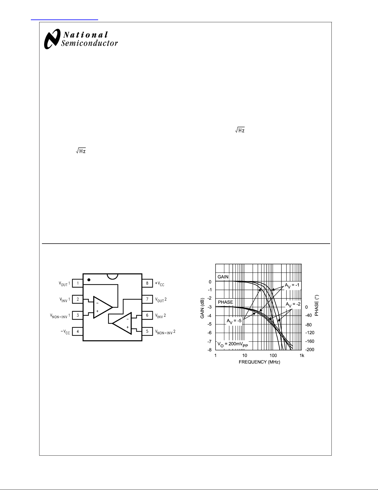
Connection Diagram
8-Pin SOIC
Top View
Inverting Frequency Response
20038535
20038515
© 2003 National Semiconductor Corporation DS200385 www.national.com
Absolute Maximum Ratings (Note 1)
If Military/Aerospace specified devices are required,
please contact the National Semiconductor Sales Office/
LMH6628
Distributors for availability and specifications.
ESD Tolerance (Note 4)
Maximum Junction Temperature +150˚C
Storage Temperature Range −65˚C to +150˚C
Lead Temperature (soldering 10 sec) +300˚C
Operating Ratings (Note 1)
Human Body Model 2kV
Machine Model 200V
Supply Voltage 13.5
Short Circuit Current (Note 3)
Common-Mode Input Voltage V
+-V−
Differential Input Voltage V+-V
−
Thermal Resistance (Note 5)
Package (θ
)(θJA)
JC
SOIC 65˚C/W 145˚C/W
Temperature Range −40˚C to +85˚C
Nominal Supply Voltage
±
Electrical Characteristics (Note 2)
VCC=±5V, AV= +2V/V, RF= 100Ω,RG= 100Ω,RL= 100Ω; unless otherwise specified. Boldface limits apply at the
temperature extremes.
Symbol Parameter Conditions Min Typ Max Units
Frequency Domain Response
GB Gain Bandwidth Product V
SSBW -3dB Bandwidth, A
SSBW -3dB Bandwidth, A
=+1 V
V
=+2 V
V
GFL Gain Flatness V
GFP Peaking DC to 200MHz 0.0 dB
GFR Rolloff DC to 20MHz .1 dB
LPD Linear Phase Deviation DC to 20MHz .1 deg
Time Domain Response
TR Rise and Fall Time 1V Step 4 ns
TS Settling Time 2V Step to 0.1% 12 ns
OS Overshoot 1V Step 1 %
SR Slew Rate 4V Step 300 550 V/µs
Distortion And Noise Response
HD2 2nd Harmonic Distortion 1V
HD3 3rd Harmonic Distortion 1V
Equivalent Input Noise
V
N
I
N
Voltage 1MHz to 100MHz 2 nV/
Current 1MHz to 100MHz 2 pA/
XTLKA Crosstalk Input Referred, 10MHz −62 dB
Static, DC Performance
G
V
DV
I
BN
DI
I
OS
I
OSD
OL
IO
IO
BN
Open-Loop Gain 56
Input Offset Voltage
Average Drift 5 µV/˚C
Input Bias Current
Average Drift 150 nA/˚C
Input Offset Current 0.3
Average Drift 5 nA/˚C
PSRR Power Supply Rejection Ratio 60
CMRR Common-Mode Rejection Ratio 57
I
CC
Supply Current Per Channel, RL=
<
0.5V
O
O
O
O
PP
<
0.5V
PP
<
0.5V
PP
<
0.5V
PP
, 10MHz −65 dBc
PP
, 10MHz −74 dBc
PP
180 300 MHz
200 MHz
100 MHz
63 dB
53
±
.5
±
.7
±
2
±
2.6
±
20
±
30
±
6µA
70 dB
46
62 dB
54
∞
7.5
7.0
912
12.5
2.5V to±6V
mV
µA
mA
www.national.com 2
Electrical Characteristics (Note 2) (Continued)
VCC=±5V, AV= +2V/V, RF= 100Ω,RG= 100Ω,RL= 100Ω; unless otherwise specified. Boldface limits apply at the
temperature extremes.
Symbol Parameter Conditions Min Typ Max Units
Miscellaneous Performance
R
IN
C
IN
R
OUT
V
O
V
OL
CMIR Input Voltage Range Common- Mode
I
O
Note 1: Absolute Maximum Ratings indicate limits beyond which damage to the device may occur. Operating Ratings indicate conditions for which the device is
intended to be functional, but specific performance is not guaranteed. For guaranteed specifications, see the Electrical Characteristics tables.
Note 2: Electrical Table values apply only for factory testing conditions at the temperature indicated. Factory testing conditions result in very limited self-heating of
the device such that T
See Note 6 for information on temperature de-rating of this device." Min/Max ratings are based on product characterization and simulation. Individual parameters
are tested as noted.
Note 3: Output is short circuit protected to ground, however maximum reliability is obtained if output current does not exceed 160mA.
Note 4: Human body model, 1.5kΩ in series with 100pF. Machine model, 0Ω In series with 200pF.
Note 5: The maximum power dissipation is a function of T
P
=(T
D
Input Resistance Common-Mode 500 kΩ
Differential-Mode 200 kΩ
Input Capacitance Common-Mode 1.5 pF
Differential-Mode 1.5 pF
Output Resistance Closed-Loop .1 Ω
Output Voltage Range RL=
RL= 100Ω
Output Current
. No guarantee of parametric performance is indicated in the electrical tables under conditions of internal self heating where T
J=TA
, θJAand TA. The maximum allowable power dissipation at any ambient temperature is
)/ θJA. All numbers apply for packages soldered directly onto a PC board.
J(MAX)-TA
J(MAX)
∞
±
3.2
±
3.1
±
50
±
3.8 V
±
3.5 V
±
3.7 V
±
85 mA
J
LMH6628
>
TA.
Ordering Information
Package Part Number Package Marking Transport Media NSC Drawing
8-pin SOIC LMH6628MA LMH6628MA Rails M08A
LMH6628MAX 2.5k Units Tape and Reel
www.national.com3
Typical Performance Characteristics (T
less specified)
LMH6628
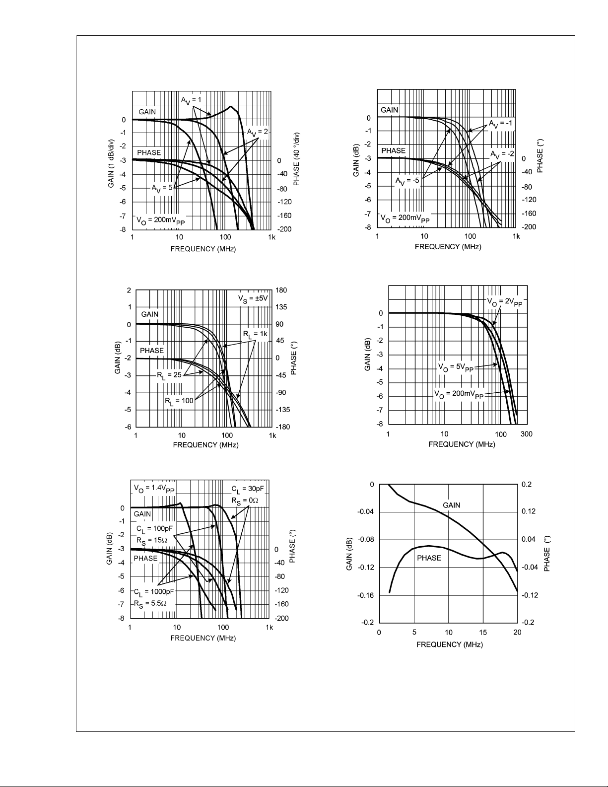
Non-Inverting Frequency Response Inverting Frequency Response
= +25˚, AV= +2, VCC=±5V, Rf=100Ω,RL= 100Ω, un-
A
20038513
20038515
Frequency Response vs. Load Resistance Frequency Response vs. Output Amplitude
20038525
20038510
Frequency Response vs. Capacitive Load Gain Flatness & Linear Phase
20038516
www.national.com 4
20038524

LMH6628
Typical Performance Characteristics (T
unless specified) (Continued)
Channel Matching Channel to Channel Crosstalk
20038514
Pulse Response (VO= 2V) Pulse Response (VO= 100mV)
= +25˚, AV= +2, VCC=±5V, Rf=100Ω,RL= 100Ω,
A
20038509
20038511 20038512
2nd Harmonic Distortion vs. Output Voltage 3rd Harmonic Distortion vs. Output Voltage
20038507 20038508
www.national.com5

Typical Performance Characteristics (T
unless specified) (Continued)
LMH6628
2nd & 3rd Harmonic Distortion vs. Frequency PSRR and CMRR (
= +25˚, AV= +2, VCC=±5V, Rf=100Ω,RL= 100Ω,
A
±
5V)
20038517
PSRR and CMRR (±2.5V) Closed Loop Output Resistance (±2.5V)
20038523 20038518
Closed Loop Output Resistance (±5V) Open Loop Gain & Phase (±2.5V)
20038522
20038519 20038521
www.national.com 6

LMH6628
Typical Performance Characteristics (T
unless specified) (Continued)
Open Loop Gain & Phase (
DC Errors vs. Temperature Maximum VOvs. R
±
5V) Recommended RSvs. C
20038520
= +25˚, AV= +2, VCC=±5V, Rf=100Ω,RL= 100Ω,
A
L
L
20038526
20038546
20038545
2-Tone, 3rd Order Intermodulation Intercept Voltage & Current Noise vs. Frequency
20038544
20038547
www.national.com7

Typical Performance Characteristics (T
unless specified) (Continued)
LMH6628
Settling Time vs. Accuracy
= +25˚, AV= +2, VCC=±5V, Rf=100Ω,RL= 100Ω,
A
20038548
Application Section
LOW NOISE DESIGN
Ultimate low noise performance from circuit designs using
the LMH6628 requires the proper selection of external resistors. By selecting appropriate low valued resistors for R
, amplifier circuits using the LMH6628 can achieve output
R
G
noise that is approximately the equivalent voltage input
noise of 2nV/
multiplied by the desired gain (AV).
DC BIAS CURRENTS AND OFFSET VOLTAGES
Cancellation of the output offset voltage due to input bias
currents is possible with the LMH6628. This is done by
making the resistance seen from the inverting and noninverting inputs equal. Once done, the residual output offset
voltage will be the input offset voltage (V
desired gain (A
). National Application Note OA-7 offers
V
) multiplied by the
OS
several solutions to further reduce the output offset.
OUTPUT AND SUPPLY CONSIDERATIONS
±
With
5V supplies, the LMH6628 is capable of a typical
output swing of
±
3.8V under a no-load condition. Additional
output swing is possible with slightly higher supply voltages.
For loads of less than 50Ω, the output swing will be limited by
the LMH6628’s output current capability, typically 85mA.
Output settling time when driving capacitive loads can be
improved by the use of a series output resistor. See the plot
labeled "R
vs. CL" in the Typical Performance section.
S
and
F
See OA-15 for more information. National suggests the
730036 (SOIC) dual op amp evaluation board as a guide for
high frequency layout and as an aid in device evaluation.
ANALOG DELAY CIRCUIT (ALL-PASS NETWORK)
The circuit in Figure 1 implements an all-pass network using
the LMH6628. A wide bandwidth buffer (LM7121) drives the
circuit and provides a high input impedance for the source.
As shown in Figure 2, the circuit provides a 13.1ns delay
(with R = 40.2Ω, C = 47pF). R
and RGshould be of equal
F
and low value for parasitic insensitive operation.
20038501
FIGURE 1.
LAYOUT
Proper power supply bypassing is critical to insure good high
frequency performance and low noise. De-coupling capacitors of 0.1µF should be placed as close as possible to the
power supply pins. The use of surface mounted capacitors is
recommended due to their low series inductance.
A good high frequency layout will keep power supply and
ground traces away from the inverting input and output pins.
Parasitic capacitance from these nodes to ground causes
frequency response peaking and possible circuit oscillation.
www.national.com 8
20038502
FIGURE 2. Delay Circuit Response to 0.5V Pulse

Application Section (Continued)
The circuit gain is +1 and the delay is determined by the
following equations.
(1)
φ
d
1
=
T
d
360
where T
is the delay of the op amp at AV= +1.
d
The LMH6628 provides a typical delay of 2.8ns at its −3dB
point.
;
df
(2)
LMH6628
20038531
FULL DUPLEX DIGITAL OR ANALOG TRANSMISSION
Simultaneous transmission and reception of analog or digital
signals over a single coaxial cable or twisted-pair line can
reduce cabling requirements. The LMH6628’s wide bandwidth and high common-mode rejection in a differential amplifier configuration allows full duplex transmission of video,
telephone, control and audio signals.
In the circuit shown in Figure 3, one of the LMH6628’s amps
is used as a "driver" and the other as a difference "receiver"
amplifier. The output impedance of the "driver" is essentially
zero. The two R’s are chosen to match the characteristic
impedance of the transmission line. The "driver" op amp gain
can be selected for unity or greater.
Receiver amplifier A
) is connected across R and forms
2(B2
differential amplifier for the signals transmitted by driver A
(B2). If RFequals RG, receiver A2(B1) will then reject the
signals from driver A
).
B
1(A1
) and pass the signals from driver
1(B1
FIGURE 4.
POSITIVE PEAK DETECTOR
The LMH6628’s dual amplifiers can be used to implement a
unity-gain peak detector circuit as shown in Figure 5.
2
20038505
FIGURE 5.
20038503
FIGURE 3.
The output of the receiver amplifier will be:
(3)
Care must be given to layout and component placement to
maintain a high frequency common-mode rejection. The plot
of Figure 4 shows the simultaneous reception of signals
transmitted at 1MHz and 10MHz.
The acquisition speed of this circuit is limited by the dynamic
resistance of the diode when charging C
. A plot of the
hold
circuit’s performance is shown in Figure 6 with a 1MHz
sinusoidal input.
www.national.com9

Application Section (Continued)
LMH6628
20038537
FIGURE 6.
A current source, built around Q1, provides the necessary
bias current for the second amplifier and prevents saturation
when power is applied. The resistor, R, closes the loop while
diode D2 prevents negative saturation when V
. A MOS-type switch (not shown) can be used to reset the
V
C
capacitor’s voltage.
The maximum speed of detection is limited by the delay of
the op amps and the diodes. The use of Schottky diodes will
provide faster response.
ADJUSTABLE OR BANDPASS EQUALIZER
A "boost" equalizer can be made with the LMH6628 by
summing a bandpass response with the input signal, as
shown in Figure 7.
is less than
IN
(4)
To build a boost circuit, use the design equations Eq. 6 and
Eq. 7.
(5)
(6)
Select R
frequency circuits - R
and C using Eq. 6. Use reasonable values for high
2
between 10Ω and 5kΩ, C between
2
10pF and 2000pF. Use Eq. 7 to determine the parallel combination of R
and Rb. Select Raand Rbby either the 10Ω to
a
5kΩ criteria or by other requirements based on the impedance V
is capable of driving. Finish the design by determin-
in
ing the value of K from Eq. 8.
(7)
Figure 8 shows an example of the response of the circuit of
Figure 9, where f
follows: R
a
is 2.3MHz. The component values are as
o
=2.1kΩ,Rb= 68.5Ω,R2= 4.22kΩ,R=500Ω,KR
=50Ω, C = 120pF.
20038506
FIGURE 7.
The overall transfer function is shown in Eq. 5.
www.national.com 10
20038543
FIGURE 8.

Physical Dimensions inches (millimeters)
unless otherwise noted
NS Package Number M08A
LMH6628 Dual Wideband, Low Noise, Voltage Feedback Op Amp
8-Pin SOIC
LIFE SUPPORT POLICY
NATIONAL’S PRODUCTS ARE NOT AUTHORIZED FOR USE AS CRITICAL COMPONENTS IN LIFE SUPPORT
DEVICES OR SYSTEMS WITHOUT THE EXPRESS WRITTEN APPROVAL OF THE PRESIDENT AND GENERAL
COUNSEL OF NATIONAL SEMICONDUCTOR CORPORATION. As used herein:
1. Life support devices or systems are devices or
systems which, (a) are intended for surgical implant
into the body, or (b) support or sustain life, and
whose failure to perform when properly used in
accordance with instructions for use provided in the
2. A critical component is any component of a life
support device or system whose failure to perform
can be reasonably expected to cause the failure of
the life support device or system, or to affect its
safety or effectiveness.
labeling, can be reasonably expected to result in a
significant injury to the user.
National Semiconductor
Americas Customer
Support Center
Email: new.feedback@nsc.com
Tel: 1-800-272-9959
www.national.com
National does not assume any responsibility for use of any circuitry described, no circuit patent licenses are implied and National reserves the right at any time without notice to change said circuitry and specifications.
National Semiconductor
Europe Customer Support Center
Fax: +49 (0) 180-530 85 86
Email: europe.support@nsc.com
Deutsch Tel: +49 (0) 69 9508 6208
English Tel: +44 (0) 870 24 0 2171
Français Tel: +33 (0) 1 41 91 8790
National Semiconductor
Asia Pacific Customer
Support Center
Fax: 65-6250 4466
Email: ap.support@nsc.com
Tel: 65-6254 4466
National Semiconductor
Japan Customer Support Center
Fax: 81-3-5639-7507
Email: nsj.crc@jksmtp.nsc.com
Tel: 81-3-5639-7560
 Loading...