

查询LMH6618MKE供应商
LMH6618 Single/LMH6619 Dual
PowerWise® 130 MHz, 1.25 mA RRIO Operational
Amplifiers
LMH6618 Single/LMH6619 Dual PowerWise130 MHz, 1.25 mA RRIO Operational Amplifiers
November 27, 2007
General Description
The LMH6618 (single, with shutdown) and LMH6619 (dual)
are 130 MHz rail-to-rail input and output amplifiers designed
for ease of use in a wide range of applications requiring high
speed, low supply current, low noise, and the ability to drive
complex ADC and video loads. The operating voltage range
extends from 2.7V to 11V and the supply current is typically
1.25 mA per channel at 5V. The LMH6618 and LMH6619 are
members of the PowerWise family and have an exceptional
power-to-performance ratio.
The amplifier’s voltage feedback design topology provides
balanced inputs and high open loop gain for ease of use and
accuracy in applications such as active filter design. Offset
voltage is typically 0.1 mV and settling time to 0.01% is 120
ns which combined with an 100 dBc SFDR at 100 kHz makes
the part suitable for use as an input buffer for popular 8-bit,
10-bit, 12-bit and 14-bit mega-sample ADCs.
The input common mode range extends 200 mV beyond the
supply rails. On a single 5V supply with a ground terminated
150Ω load the output swings to within 37 mV of the ground
rail, while a mid-rail terminated 1 kΩ load will swing to 77 mV
of either rail, providing true single supply operation and maximum signal dynamic range on low power rails. The amplifier
output will source and sink 35 mA and drive up to 30 pF loads
without the need for external compensation.
The LMH6618 has an active low disable pin which reduces
the supply current to 72 µA and is offered in the space saving
6-Pin TSOT23 package. The LMH6619 is offered in the 8-Pin
SOIC package. The LMH6618 and LMH6619 are available
with a −40°C to +125°C extended industrial temperature
grade.
Features
VS = 5V, RL = 1 kΩ, TA = 25°C and AV = +1, unless otherwise
specified.
Operating voltage range 2.7V to 11V
■
Supply current per channel 1.25 mA
■
Small signal bandwidth 130 MHz
■
Slew rate 55 V/µs
■
Settling time to 0.1% 90 ns
■
Settling time to 0.01% 120 ns
■
SFDR (f = 100 kHz, AV = +1, V
■
0.1 dB bandwidth (AV = +2) 15 MHz
■
Low voltage noise 10 nV/√Hz
■
Industrial temperature grade −40°C to +125°C
■
Rail-to-Rail input and output
■
= 2 VPP) 100 dBc
OUT
Applications
ADC driver
■
DAC buffer
■
Active filters
■
High speed sensor amplifier
■
Current sense amplifier
■
Portable video
■
STB, TV video amplifier
■
Typical Application
PowerWise® is a registered trademark of National Semiconductor.
WEBENCH® is a registered trademark of National Semiconductor Corporation.
© 2007 National Semiconductor Corporation 201958 www.national.com
20195829
Absolute Maximum Ratings (Note 1)
If Military/Aerospace specified devices are required,
please contact the National Semiconductor Sales Office/
Distributors for availability and specifications.
ESD Tolerance (Note 2)
Human Body Model
For input pins only 2000V
LMH6618/LMH6619
For all other pins 2000V
Machine Model 200V
Supply Voltage (VS = V+ – V−)
12V
Junction Temperature (Note 3) 150°C max
Operating Ratings (Note 1)
Supply Voltage (VS = V+ – V−)
Ambient Temperature Range (Note 3) −40°C to +125°C
Package Thermal Resistance (θJA)
6-Pin TSOT23 231°C/W
8-Pin SOIC 160°C/W
2.7V to 11V
+3V Electrical Characteristics Unless otherwise specified, all limits are guaranteed for T
= +25°C,
J
V+ = 3V, V− = 0V, DISABLE = 3V, VCM = VO = V+/2, AV = +1 (RF = 0Ω), otherwise RF = 2 kΩ for AV ≠ +1, RL = 1 kΩ || 5 pF.
Boldface Limits apply at temperature extremes. (Note 4)
Symbol Parameter Condition Min
(Note 8)
Typ
(Note 7)
Max
(Note 8)
Units
Frequency Domain Response
SSBW –3 dB Bandwidth Small Signal
GBW Gain Bandwidth
LSBW −3 dB Bandwidth Large Signal
AV = 1, RL = 1 kΩ, V
AV = 2, −1, RL = 1 kΩ, V
OUT
= 0.2 V
= 0.2 V
OUT
AV = 10, RF = 2 kΩ, RG = 221Ω,
RL = 1 kΩ, V
AV = 1, RL = 1 kΩ, V
AV = 2, RL = 150Ω, V
OUT
= 0.2 V
OUT
OUT
PP
= 2 V
= 2 V
PP
PP
PP
PP
120
56
MHz
55 71 MHz
13
13
MHz
Peak Peaking AV = 1, CL = 5 pF 1.5 dB
0.1
dBBW
DG Differential Gain AV = +2, 4.43 MHz, 0.6V < V
0.1 dB Bandwidth AV = 2, V
RF = RG = 825Ω
= 0.5 VPP ,
OUT
OUT
< 2V,
15 MHz
0.1 %
RL = 150Ω to V+/2
DP Differential Phase AV = +2, 4.43 MHz, 0.6V < V
OUT
< 2V,
0.1 deg
RL = 150Ω to V+/2
Time Domain Response
tr/t
f
SR Slew Rate 2V Step, AV = 1 36 46
t
s_0.1
t
s_0.01
Rise & Fall Time 2V Step, AV = 1 36 ns
V/μs
0.1% Settling Time 2V Step, AV = −1 90
0.01% Settling Time 2V Step, AV = −1 120
ns
Noise and Distortion Performance
SFDR Spurious Free Dynamic Range
e
n
i
n
Input Voltage Noise f = 100 kHz 10
Input Current Noise f = 100 kHz 1
fC = 100 kHz, V
fC = 1 MHz, V
fC = 5 MHz, V
OUT
= 2 VPP, RL = 1 kΩ
OUT
= 2 VPP, RL = 1 kΩ
OUT
CT Crosstalk (LMH6619) f = 5 MHz, VIN = 2 V
= 2 VPP, RL = 1 kΩ
PP
100
61
dBc
47
nV/
pA/
80 dB
Input, DC Performance
V
OS
TCV
I
B
I
O
C
IN
R
IN
Input Offset Voltage VCM = 0.5V (pnp active)
0.1 ±0.6
VCM = 2.5V (npn active)
Input Offset Voltage Average Drift (Note 5) 0.8
OS
Input Bias Current VCM = 0.5V (pnp active) −1.4 −2.6
VCM = 2.5V (npn active) +1.0 +1.8
Input Offset Current 0.01 ±0.27
Input Capacitance 1.5 pF
Input Resistance 8
±1.0
mV
μV/°C
μA
μA
MΩ
www.national.com 2
LMH6618/LMH6619
Symbol Parameter Condition Min
(Note 8)
CMVR Input Voltage Range
DC, CMRR ≥ 65 dB
−0.2 3.2 V
CMRR Common Mode Rejection Ratio VCM Stepped from −0.1V to 1.4V 78 96
VCM Stepped from 2.0V to 3.1V 81 107
A
OL
Open Loop Gain
RL = 1 kΩ to +2.7V or +0.3V
RL = 150Ω to +2.6V or +0.4V
85 98
76 82
Typ
(Note 7)
Max
(Note 8)
Units
dB
dB
Output DC Characteristics
V
O
Output Swing High (LMH6618)
(Voltage from V+ Supply Rail)
RL = 1 kΩ to V+/2
RL =150Ω to V+/2
56
62
172
50
160
198
Output Swing Low (LMH6618)
(Voltage from V− Supply Rail)
RL = 1 kΩ to V+/2
RL = 150Ω to V+/2
60 66
74
170 184
mV
217
RL = 150Ω to V
−
29 39
43
Output Swing High (LMH6619)
(Voltage from V+ Supply Rail)
RL = 1 kΩ to V+/2
RL =150Ω to V+/2
56
62
172
50
160
198
Output Swing Low (LMH6619)
(Voltage from V− Supply Rail)
RL = 1 kΩ to V+/2
RL =150Ω to V+/2
62 68
76
175 189
mV
222
RL = 150Ω to V
−
34 44
48
I
R
OUT
O
Linear Output Current V
= V+/2 (Note 6) ±25 ±35 mA
OUT
Output Resistance f = 1 MHz 0.17
Enable Pin Operation
Enable High Voltage Threshold Enabled 2.0 V
Enable Pin High Current V
= 3V 0.04 µA
DISABLE
Enable Low Voltage Threshold Disabled 1.0 V
Enable Pin Low Current V
t
on
t
off
Turn-On Time 25 ns
Turn-Off Time 90 ns
= 0V 1 µA
DISABLE
Power Supply Performance
PSRR Power Supply Rejection Ratio DC, VCM = 0.5V, VS = 2.7V to 11V 84 104 dB
I
S
I
SD
Supply Current (LMH6618)
RL = ∞
1.2 1.5
1.7
Supply Current (LMH6619)
(per channel)
RL = ∞
1.2 1.5
1.75
Disable Shutdown Current DISABLE = 0V 59 85
mA
μA
Ω
3 www.national.com
+5V Electrical Characteristics Unless otherwise specified, all limits are guaranteed for T
= +25°C,
J
V+ = 5V, V− = 0V, DISABLE = 5V, VCM = VO = V+/2, AV = +1 (RF = 0Ω), otherwise RF = 2 kΩ for AV ≠ +1, RL = 1 kΩ || 5 pF.
Boldface Limits apply at temperature extremes.
Symbol Parameter Condition Min
(Note 8)
Typ
(Note 7)
Max
(Note 8)
Frequency Domain Response
SSBW –3 dB Bandwidth Small Signal
LMH6618/LMH6619
GBW Gain Bandwidth
LSBW −3 dB Bandwidth Large Signal
AV = 1, RL = 1 kΩ, V
AV = 2, −1, RL = 1 kΩ, V
OUT
= 0.2 V
= 0.2 V
OUT
AV = 10, RF = 2 kΩ, RG = 221Ω,
RL = 1 kΩ, V
AV = 1, RL = 1 kΩ, V
AV = 2, RL = 150Ω, V
OUT
= 0.2 V
OUT
OUT
PP
= 2 V
= 2 V
PP
PP
PP
PP
130
53
54 64 MHz
15
15
Peak Peaking AV = 1, CL = 5 pF 0.5 dB
0.1
dBBW
DG Differential Gain AV = +2, 4.43 MHz, 0.6V < V
0.1 dB Bandwidth AV = 2, V
RF = RG = 1 kΩ
= 0.5 VPP,
OUT
OUT
< 2V,
15 MHz
0.1 %
RL = 150Ω to V+/2
DP Differential Phase AV = +2, 4.43 MHz, 0.6V < V
OUT
< 2V,
0.1 deg
RL = 150Ω to V+/2
Time Domain Response
tr/t
f
Rise & Fall Time 2V Step, AV = 1 30 ns
SR Slew Rate 2V Step, AV = 1 44 55
t
s_0.1
t
s_0.01
0.1% Settling Time 2V Step, AV = −1 90
0.01% Settling Time 2V Step, AV = −1 120
Distortion and Noise Performance
SFDR Spurious Free Dynamic Range
fC = 100 kHz, V
fC = 1 MHz, V
OUT
= 2 VPP, RL = 1 kΩ
OUT
fC = 5 MHz, VO = 2 VPP, RL = 1 kΩ
e
n
i
n
Input Voltage Noise f = 100 kHz 10
Input Current Noise f = 100 kHz 1
CT Crosstalk (LMH6619) f = 5 MHz, VIN = 2 V
= 2 VPP, RL = 1 kΩ
PP
100
88
61
80 dB
Input, DC Performance
V
OS
TCV
I
B
Input Offset Voltage VCM = 0.5V (pnp active)
VCM = 4.5V (npn active)
Input Offset Voltage Average Drift (Note 5) 0.8 µV/°C
OS
0.1 ±0.6
±1.0
Input Bias Current VCM = 0.5V (pnp active) −1.5 −2.4
VCM = 4.5V (npn active) +1.0 +1.9
I
O
C
IN
R
IN
CMVR Input Voltage Range
Input Offset Current 0.01 ±0.26
Input Capacitance 1.5 pF
Input Resistance 8
DC, CMRR ≥ 65 dB
−0.2 5.2 V
CMRR Common Mode Rejection Ratio VCM Stepped from −0.1V to 3.4V 81 98
VCM Stepped from 4.0V to 5.1V 84 108
A
OL
Open Loop Gain
RL = 1 kΩ to +4.6V or +0.4V
RL = 150Ω to +4.5V or +0.5V
84 100
78 83
Units
MHz
MHz
V/μs
ns
dBc
nV/
pA/
mV
μA
μA
MΩ
dB
dB
www.national.com 4
LMH6618/LMH6619
Symbol Parameter Condition Min
(Note 8)
Typ
(Note 7)
Max
(Note 8)
Units
Output DC Characteristics
V
O
Output Swing High (LMH6618)
(Voltage from V+ Supply Rail)
RL = 1 kΩ to V+/2
RL = 150Ω to V+/2
73
82
255
60
230
295
Output Swing Low (LMH6618)
(Voltage from V− Supply Rail)
RL = 1 kΩ to V+/2
RL = 150Ω to V+/2
75 83
96
250 270
mV
321
RL = 150Ω to V
−
32 43
45
Output Swing High (LMH6619)
(Voltage from V+ Supply Rail)
RL = 1 kΩ to V+/2
RL = 150Ω to V+/2
73
82
255
60
230
295
Output Swing Low (LMH6619)
(Voltage from V− Supply Rail)
RL = 1 kΩ to V+/2
RL = 150Ω to V+/2
77 85
98
255 275
mV
326
RL = 150Ω to V
−
37 48
50
I
R
OUT
O
Linear Output Current V
= V+/2 (Note 6) ±25 ±35 mA
OUT
Output Resistance f = 1 MHz 0.17
Ω
Enable Pin Operation
Enable High Voltage Threshold Enabled 3.0 V
Enable Pin High Current V
= 5V 1.2 µA
DISABLE
Enable Low Voltage Threshold Disabled 2.0 V
Enable Pin Low Current V
t
on
t
off
Turn-On Time 25 ns
Turn-Off Time 90 ns
= 0V 2.5 µA
DISABLE
Power Supply Performance
PSRR Power Supply Rejection Ratio DC, VCM = 0.5V, VS = 2.7V to 11V 84 104 dB
I
S
I
SD
Supply Current (LMH6618)
RL = ∞
1.25 1.5
1.7
Supply Current (LMH6619)
(per channel)
RL = ∞
1.3 1.5
1.75
Disable Shutdown Current DISABLE = 0V 72 105
mA
μA
±5V Electrical Characteristics Unless otherwise specified, all limits are guaranteed for T
= +25°C,
J
V+ = 5V, V− = −5V, DISABLE = 5V, VCM = VO = 0V, AV = +1 (RF = 0Ω), otherwise RF = 2 kΩ for AV ≠ +1, RL = 1 kΩ || 5 pF.
Boldface Limits apply at temperature extremes.
Symbol Parameter Condition Min
(Note 8)
Typ
(Note 7)
Max
(Note 8)
Frequency Domain Response
SSBW –3 dB Bandwidth Small Signal
GBW Gain Bandwidth
LSBW −3 dB Bandwidth Large Signal
AV = 1, RL = 1 kΩ, V
AV = 2, −1, RL = 1 kΩ, V
OUT
= 0.2 V
= 0.2 V
OUT
AV = 10, RF = 2 kΩ, RG = 221Ω,
RL = 1 kΩ, V
AV = 1, RL = 1 kΩ, V
AV = 2, RL = 150Ω, V
= 0.2 V
OUT
PP
= 2 V
OUT
= 2 V
OUT
5 www.national.com
PP
PP
PP
PP
140
53
54 65 MHz
16
15
Units
MHz
MHz
Symbol Parameter Condition Min
(Note 8)
Typ
(Note 7)
Max
(Note 8)
Peak Peaking AV = 1, CL = 5 pF 0.05 dB
0.1
dBBW
DG Differential Gain AV = +2, 4.43 MHz, 0.6V < V
LMH6618/LMH6619
DP Differential Phase AV = +2, 4.43 MHz, 0.6V < V
0.1 dB Bandwidth AV = 2, V
RF = RG = 1.21 kΩ
RL = 150Ω to V+/2
= 0.5 VPP,
OUT
OUT
OUT
< 2V,
< 2V,
15 MHz
0.1 %
0.1 deg
RL = 150Ω to V+/2
Time Domain Response
tr/t
f
Rise & Fall Time 2V Step, AV = 1 30 ns
SR Slew Rate 2V Step, AV = 1 45 57
t
s_0.1
t
s_0.01
0.1% Settling Time 2V Step, AV = −1 90
0.01% Settling Time 2V Step, AV = −1 120
Noise and Distortion Performance
SFDR Spurious Free Dynamic Range
e
n
i
n
Input Voltage Noise f = 100 kHz 10
Input Current Noise f = 100 kHz 1
fC = 100 kHz, V
fC = 1 MHz, V
fC = 5 MHz, V
OUT
= 2 VPP, RL = 1 kΩ
OUT
= 2 VPP, RL = 1 kΩ
OUT
CT Crosstalk (LMH6619) f = 5 MHz, VIN = 2 V
= 2 VPP, RL = 1 kΩ
PP
100
88
70
80 dB
Input DC Performance
V
OS
TCV
I
B
Input Offset Voltage VCM = −4.5V (pnp active)
VCM = 4.5V (npn active)
Input Offset Voltage Average Drift (Note 5) 0.9 µV/°C
OS
0.1 ±0.6
±1.0
Input Bias Current VCM = −4.5V (pnp active) −1.5 −2.4
VCM = 4.5V (npn active) +1.0 +1.9
I
O
C
IN
R
IN
CMVR Input Voltage Range
Input Offset Current 0.01 ±0.26
Input Capacitance 1.5 pF
Input Resistance 8
DC, CMRR ≥ 65 dB
−5.2 5.2 V
CMRR Common Mode Rejection Ratio VCM Stepped from −5.1V to 3.4V 84 100
VCM Stepped from 4.0V to 5.1V 83 108
A
OL
Open Loop Gain
RL = 1 kΩ to +4.6V or −4.6V
RL = 150Ω to +4.3V or −4.3V
86 95
79 84
Units
V/μs
ns
dBc
nV/
pA/
mV
μA
μA
MΩ
dB
dB
www.national.com 6
LMH6618/LMH6619
Symbol Parameter Condition Min
(Note 8)
Typ
(Note 7)
Max
(Note 8)
Units
Output DC Characteristics
V
O
Output Swing High (LMH6618)
(Voltage from V+ Supply Rail)
RL = 1 kΩ to GND
RL = 150Ω to GND
111
126
457
100
430
526
Output Swing Low (LMH6618)
(Voltage from V− Supply Rail)
RL = 1 kΩ to GND
RL = 150Ω to GND
110 121
136
440 474
mV
559
RL = 150Ω to V
−
35 51
52
Output Swing High (LMH6619)
(Voltage from V+ Supply Rail)
RL = 1 kΩ to GND
RL = 150Ω to GND
111
126
457
100
430
526
Output Swing Low (LMH6619)
(Voltage from V− Supply Rail)
RL = 1 kΩ to GND
RL = 150Ω to GND
115 126
141
450 484
mV
569
RL = 150Ω to V
−
45 61
62
I
R
OUT
O
Linear Output Current V
= V+/2 (Note 6) ±25 ±35 mA
OUT
Output Resistance f = 1 MHz 0.17
Ω
Enable Pin Operation
Enable High Voltage Threshold Enabled 0.5 V
Enable Pin High Current V
= +5V 16 µA
DISABLE
Enable Low Voltage Threshold Disabled −0.5 V
Enable Pin Low Current V
t
on
t
off
Turn-On Time 25 ns
Turn-Off Time 90 ns
= −5V 17 µA
DISABLE
Power Supply Performance
PSRR Power Supply Rejection Ratio DC, VCM = −4.5V, VS = 2.7V to 11V 84 104 dB
I
S
I
SD
Supply Current (LMH6618)
RL = ∞
1.35 1.6
1.9
Supply Current (LMH6619)
(per channel)
RL = ∞
1.45 1.65
2.0
Disable Shutdown Current DISABLE = −5V 103 140
mA
μA
Note 1: Absolute Maximum Ratings indicate limits beyond which damage to the device may occur. Operating Ratings indicate conditions for which the device is
intended to be functional, but specific performance is not guaranteed. For guaranteed specifications and the test conditions, see the Electrical Characteristics.
Note 2: Human Body Model, applicable std. MIL-STD-883, Method 3015.7. Machine Model, applicable std. JESD22-A115-A (ESD MM std. of JEDEC)
Field-Induced Charge-Device Model, applicable std. JESD22-C101-C (ESD FICDM std. of JEDEC).
Note 3: The maximum power dissipation is a function of T
PD = (T
Note 4: Boldface limits apply to temperature range of −40°C to 125°C
Note 5: Voltage average drift is determined by dividing the change in VOS by temperature change.
Note 6: Do not short circuit the output. Continuous source or sink currents larger than the I
Note 7: Typical values represent the most likely parametric norm as determined at the time of characterization. Actual typical values may vary over time and will
also depend on the application and configuration. The typical values are not tested and are not guaranteed on shipped production material.
Note 8: Limits are 100% production tested at 25°C. Limits over the operating temperature range are guaranteed through correlations using the Statistical Quality
Control (SQC) method.
) – TA)/ θJA. All numbers apply for packages soldered directly onto a PC Board.
J(MAX
, θJA. The maximum allowable power dissipation at any ambient temperature is
J(MAX)
typical are not recommended as it may damage the part.
OUT
7 www.national.com
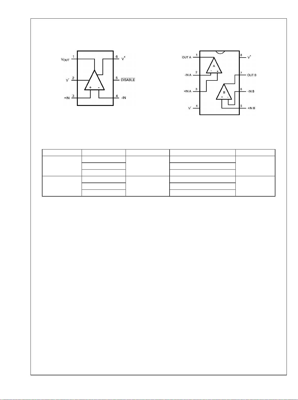
Connection Diagrams
LMH6618/LMH6619
Ordering Information
Package Part Number Package Marking Transport Media NSC Drawing
6-Pin TSOT23
8-Pin SOIC
6-Pin TSOT23
Top View
LMH6618MK
LMH6618MKX 3k Units Tape and Reel
LMH6619MA
LMH6619MAX 2.5k Units Tape and Reel
20195801
1k Units Tape and Reel
AE4A
95 Units/Rail
LMH6619MA
8-Pin SOIC
Top View
20195878
MK06ALMH6618MKE 250 Units Tape and Reel
M08ALMH6619MAE 250 Units Tape and Reel
www.national.com 8
LMH6618/LMH6619
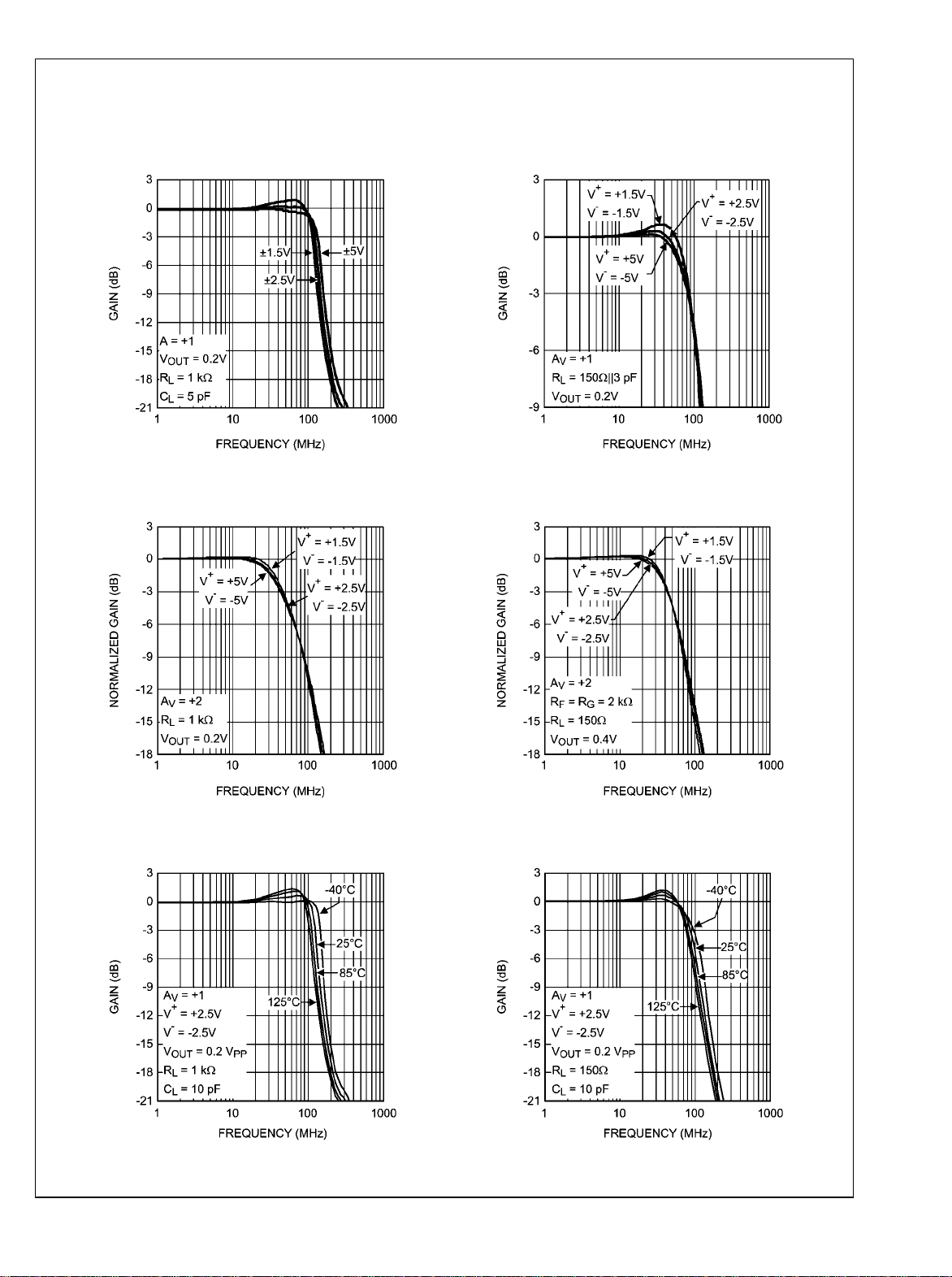
Typical Performance Characteristics At T
unless otherwise specified.
Closed Loop Frequency Response for
Various Supplies
20195831
Closed Loop Frequency Response for
Various Supplies
= 25°C, AV = +1 (RF = 0Ω), otherwise RF = 2 kΩ for AV ≠ +1,
J
Closed Loop Frequency Response for
Various Supplies
20195816
Closed Loop Frequency Response for
Various Supplies
Closed Loop Frequency Response for
Various Temperatures
20195819
20195815
20195817
Closed Loop Frequency Response for
Various Temperatures
20195820
9 www.national.com

Closed Loop Gain vs. Frequency for
LMH6618/LMH6619
Various Gains
Large Signal Frequency Response
20195830
±0.1 dB Gain Flatness for Various Supplies
20195832
Small Signal Frequency Response with
Capacitive Load and Various R
ISO
20195818
Small Signal Frequency Response with
Various Capacitive Load
20195826
HD2 vs. Frequency and Supply Voltage
20195827
www.national.com 10
20195835

LMH6618/LMH6619
HD3 vs. Frequency and Supply Voltage
20195836
HD2 and HD3 vs. Common Mode Voltage
HD2 and HD3 vs. Frequency and Load
20195871
HD2 and HD3 vs. Common Mode Voltage
HD2 vs. Frequency and Gain
20195872
20195874
20195873
HD3 vs. Frequency and Gain
20195875
11 www.national.com

LMH6618/LMH6619
Open Loop Gain/Phase
HD2 vs. Output Swing
HD3 vs. Output Swing
HD2 vs. Output Swing
20195833
20195844
20195843
HD2 vs. Output Swing
20195845
HD3 vs. Output Swing
20195869
www.national.com 12
20195846

LMH6618/LMH6619
HD3 vs. Output Swing
20195870
Settling Time vs. Input Step Amplitude
(Output Slew and Settle Time)
THD vs. Output Swing
20195847
Input Noise vs. Frequency
VOS vs. V
OUT
20195821
20195849
VOS vs. V
20195876
OUT
20195850
13 www.national.com

LMH6618/LMH6619
VOS vs. V
CM
VOS vs. VS (pnp)
VOS vs. VS (npn)
VOS Distribution (pnp and npn)
20195851
20195853
VOS vs. I
OUT
IB vs. VS (pnp)
20195852
20195854
20195877
www.national.com 14
20195855

LMH6618/LMH6619
IB vs. VS (npn)
V
vs. V
OUT
S
20195856
IS vs. V
V
OUT
vs. V
S
20195857
S
20195858
V
OUT
vs. V
S
20195860
Closed Loop Output Impedance vs. Frequency AV = +1
20195859
20195822
15 www.national.com

LMH6618/LMH6619
PSRR vs. Frequency
PSRR vs. Frequency
CMRR vs. Frequency
Small Signal Step Response
20195837
20195823
20195838
Crosstalk Rejection vs. Frequency (Output to Output)
20195879
Small Signal Step Response
20195805
www.national.com 16
20195806

LMH6618/LMH6619
Small Signal Step Response
Small Signal Step Response
20195804
Small Signal Step Response
20195808
Small Signal Step Response
Small Signal Step Response
20195809
20195811
20195807
Small Signal Step Response
20195812
17 www.national.com

Small Signal Step Response
LMH6618/LMH6619
Large Signal Step Response
Large Signal Step Response
IS vs. V
DISABLE
20195810
20195814
20195813
Overload Recovery Waveform
20195824
20195861
www.national.com 18

LMH6618/LMH6619
Application Information
The LMH6618 and LMH6619 are based on National
Semiconductor’s proprietary VIP10 dielectrically isolated
bipolar process. This device family architecture features the
following:
•
Complimentary bipolar devices with exceptionally high f
(∼8 GHz) even under low supply voltage (2.7V) and low
bias current.
•
Common emitter push-push output stage. This
architecture allows the output to reach within millivolts of
either supply rail.
•
Consistent performance from any supply voltage
with little variation with supply voltage for the most
11V)
important specifications (e.g. BW, SR, I
•
Significant power saving compared to competitive devices
OUT
on the market with similar performance.
With 3V supplies and a common mode input voltage range
that extends beyond either supply rail, the LMH6618 and
LMH6619 are well suited to many low voltage/low power applications. Even with 3V supplies, the −3 dB BW
(at AV = +1) is typically 120 MHz.
The LMH6618 and LMH6619 are designed to avoid output
phase reversal. With input over-drive, the output is kept near
the supply rail (or as close to it as mandated by the closed
loop gain setting and the input voltage). Figure 1 shows the
input and output voltage when the input voltage significantly
exceeds the supply voltages.
(2.7V -
.)
100 µA. The DISABLE pin is “active low” and should be connected through a resistor to V+ for normal operation. Shutdown is guaranteed when the DISABLE pin is 0.5V below the
supply midpoint at any operating supply voltage and temperature.
In the shutdown mode, essentially all internal device biasing
t
is turned off in order to minimize supply current flow and the
output goes into high impedance mode. During shutdown, the
input stage has an equivalent circuit as shown in Figure 2.
20195839
FIGURE 2. Input Equivalent Circuit During Shutdown
20195825
FIGURE 1. Input and Output Shown with CMVR Exceeded
If the input voltage range is exceeded by more than a diode
drop beyond either rail, the internal ESD protection diodes will
start to conduct. The current flow in these ESD diodes should
be externally limited.
The LMH6618 can be shutdown by connecting the
DISABLE pin to a voltage 0.5V below the supply midpoint
which will reduce the supply current to typically less than
When the LMH6618 is shutdown, there may be current flow
through the internal diodes shown, caused by input potential,
if present. This current may flow through the external feedback resistor and result in an apparent output signal. In most
shutdown applications the presence of this output is inconsequential. However, if the output is “forced” by another device, the other device will need to conduct the current
described in order to maintain the output potential.
To keep the output at or near ground during shutdown when
there is no other device to hold the output low, a switch using
a transistor can be used to shunt the output to ground.
SINGLE CHANNEL ADC DRIVER
The low noise and wide bandwidth make the LMH6618 an
excellent choice for driving a 12-bit ADC. Figure 3 shows the
schematic of the LMH6618 driving an ADC121S101. The ADC121S101 is a single channel 12-bit ADC. The LMH6618 is
set up in a 2nd order multiple-feedback configuration with a
gain of −1. The −3 dB point is at 500 kHz and the −0.01 dB
point is at 100 kHz. The 22Ω resistor and 390 pF capacitor
form an antialiasing filter for the ADC121S101. The capacitor
also stores and delivers charge to the switched capacitor input of the ADC. The capacitive load on the LMH6618 created
by the 390 pF capacitor is decreased by the 22Ω resistor.
Table 1 shows the performance data of the LMH6618 and the
ADC121S101.
19 www.national.com

LMH6618/LMH6619
FIGURE 3. LMH6618 Driving an ADC121S101
TABLE 1. Performance Data for the LMH6618 Driving an ADC121S101
Parameter Measured Value
Signal Frequency 100 kHz
Signal Amplitude 4.5V
SINAD 71.5 dB
SNR 71.87 dB
THD −82.4 dB
SFDR 90.97 dB
ENOB 11.6 bits
20195829
www.national.com 20

LMH6618/LMH6619
When the op amp and the ADC are using the same supply, it
is important that both devices are well bypassed. A 0.1 µF
ceramic capacitor and a 10 µF tantalum capacitor should be
located as close as possible to each supply pin. A sample
FIGURE 4. LMH6618 and ADC121S101 Layout
SINGLE TO DIFFERENTIAL ADC DRIVER
Figure 5 shows the LMH6619 used to drive a differential ADC
with a single-ended input. The ADC121S625 is a fully differ-
layout is shown in Figure 4. The 0.1 µF capacitors (C13 and
C6) and the 10 µF capacitors (C11 and C5) are located very
close to the supply pins of the LMH6618 and the
ADC121S101.
20195840
ential 12-bit ADC. Table 2 shows the performance data of the
LMH6619 and the ADC121S625.
FIGURE 5. LMH6619 Driving an ADC121S625
21 www.national.com
20195880

TABLE 2. Performance Data for the LMH6619 Driving an ADC121S625
Parameter Measured Value
Signal Frequency 10 kHz
Signal Amplitude 2.5V
SINAD 67.9 dB
SNR 68.29 dB
LMH6618/LMH6619
THD −78.6 dB
SFDR 75.0 dB
ENOB 11.0 bits
DIFFERENTIAL ADC DRIVER
The circuit in Figure 3 can be used to drive both inputs of a
differential ADC. Figure 6 shows the LMH6619 driving an AD-
C121S705. The ADC121S705 is a fully differential 12-bit
ADC. Performance with this circuit is similar to the circuit in
Figure 3.
FIGURE 6. LMH6619 Driving an ADC121S705
www.national.com 22
20195842

LMH6618/LMH6619
DC LEVEL SHIFTING
Often a signal must be both amplified and level shifted while
using a single supply for the op amp. The circuit in Figure 7
can do both of these tasks. The procedure for specifying the
resistor values is as follows.
1.
Determine the input voltage.
2.
Calculate the input voltage midpoint, V
(V
– V
INMAX
3.
Determine the output voltage needed.
4.
Calculate the output voltage midpoint, V
V
OUTMIN
5.
Calculate the gain needed, gain = (V
(V
– V
INMAX
6.
Calculate the amount the voltage needs to be shifted
from input to output, ΔV
7.
Set the supply voltage to be used.
8.
Calculate the noise gain, noise gain = gain + ΔV
9.
Set RF.
10.
Calculate R1, R1 = RF/gain.
11.
Calculate R2, R2 = RF/(noise gain-gain).
12.
Calculate RG, RG= RF/(noise gain – 1).
Check that both the VIN and V
ranges of the LMH6618.
+ (V
INMIN
OUTMAX
INMIN
)/2.
)
– V
)/2.
OUTMIN
= V
OUT
OUTMID
are within the voltage
OUT
= V
INMID
OUTMID
– V
OUTMAX
– gain x V
INMIN
=
OUTMIN
INMID
OUT/VS
+
.
The following example is for a VIN of 0V to 1V with a V
2V to 4V.
1.
VIN = 0V to 1V
2.
V
= 0V + (1V – 0V)/2 = 0.5V
INMID
3.
V
= 2V to 4V
OUT
4.
V
= 2V + (4V – 2V)/2 = 3V
OUTMID
5.
Gain = (4V – 2V)/(1V – 0V) = 2
6.
ΔV
= 3V – 2 x 0.5V = 2
OUT
7.
For the example the supply voltage will be +5V.
8.
Noise gain = 2 + 2/5V = 2.4
9.
)/
RF = 2 kΩ
10.
R1 = 2 kΩ/2 = 1 kΩ
11.
R2 = 2 kΩ/(2.4-2) = 5 kΩ
12.
RG = 2 kΩ/(2.4 – 1) = 1.43 kΩ
OUT
of
.
4th ORDER MULTIPLE FEEDBACK LOW-PASS FILTER
Figure 8 shows the LMH6619 used as the amplifier in a multiple feedback low pass filter. This filter is set up to have a gain
of +1 and a −3 dB point of 1 MHz. Values can be determined
20195848
FIGURE 7. DC Level Shifting
by using the WEBENCH® Active Filter Designer found at
amplifiers.national.com.
FIGURE 8. 4th Order Multiple Feedback Low-Pass Filter
23 www.national.com
20195828

CURRENT SENSE AMPLIFIER
With it’s rail-to-rail input and output capability, low VOS, and
low IB the LMH6618 is an ideal choice for a current sense
amplifier application. Figure 9 shows the schematic of the
LMH6618 set up in a low-side sense configuration which provides a conversion gain of 2V/A. Voltage error due to VOS can
be calculated to be VOS x (1 + RF/RG) or
0.6 mV x 21 = 12.6 mV. Voltage error due to IO is IO x RF or
LMH6618/LMH6619
0.26 µA x 1 kΩ = 0.26 mV. Hence total voltage error is
12.6 mV + 0.26 mV or 12.86 mV which translates into a current error of 12.86 mV/(2 V/A) = 6.43 mA.
FIGURE 9. Current Sense Amplifier
TRANSIMPEDANCE AMPLIFIER
By definition, a photodiode produces either a current or voltage output from exposure to a light source. A Transimpedance Amplifier (TIA) is utilized to convert this low-level
current to a usable voltage signal. The TIA often will need to
be compensated to insure proper operation.
(1)
(2)
20195841
20195865
FIGURE 11. Bode Plot of Noise Gain Intersecting with Op
Amp Open-Loop Gain
Figure 11 shows the bode plot of the noise gain intersecting
the op amp open loop gain. With larger values of gain, CT and
RF create a zero in the transfer function. At higher frequencies
the circuit can become unstable due to excess phase shift
around the loop.
A pole at fP in the noise gain function is created by placing a
feedback capacitor (CF) across RF. The noise gain slope is
flattened by choosing an appropriate value of CF for optimum
performance.
Theoretical expressions for calculating the optimum value of
CF and the expected −3 dB bandwidth are:
20195862
FIGURE 10. Photodiode Modeled with Capacitance
Elements
Figure 10 shows the LMH6618 modeled with photodiode and
the internal op amp capacitances. The LMH6618 allows circuit operation of a low intensity light due to its low input bias
current by using larger values of gain (RF). The total capacitance (CT) on the inverting terminal of the op amp includes
the photodiode capacitance (CPD) and the input capacitance
of the op amp (CIN). This total capacitance (CT) plays an important role in the stability of the circuit. The noise gain of this
circuit determines the stability and is defined by:
www.national.com 24
(3)
(4)
Equation 4 indicates that the −3 dB bandwidth of the TIA is
inversely proportional to the feedback resistor. Therefore, if
the bandwidth is important then the best approach would be
to have a moderate transimpedance gain stage followed by a
broadband voltage gain stage.
Table 3 shows the measurement results of the LMH6618 with
different photodiodes having various capacitances (CPD) and
a feedback resistance (RF) of 1 kΩ.

TABLE 3. TIA (Figure 1) Compensation and Performance Results
LMH6618/LMH6619
C
PD
C
T
C
F CAL
C
F USED
f
−3 dB CAL
f
−3 dB MEAS
(pF) (pF) (pF) (pF) (MHz) (MHz) (dB)
22 24 7.7 5.6 23.7 20 0.9
47 49 10.9 10 16.6 15.2 0.8
100 102 15.8 15 11.5 10.8 0.9
222 224 23.4 18 7.81 8 2.9
Note:
GBWP = 65 MHz
CT = CPD + C
CIN = 2 pF
VS = ±2.5V
Figure 12 shows the frequency response for the various photodiodes in Table 3.
IN
noise voltage, feedback resistor thermal noise, input noise
current, photodiode noise current) do not all operate over the
same frequency band. Therefore, when the noise at the output is calculated, this should be taken into account. The op
amp noise voltage will be gained up in the region between the
noise gain’s zero and pole (fZ and fP in Figure 11). The higher
the values of RF and CT, the sooner the noise gain peaking
starts and therefore its contribution to the total output noise
will be larger. It is obvious to note that it is advantageous to
minimize CIN by proper choice of op amp or by applying a
reverse bias across the diode at the expense of excess dark
current and noise.
DIFFERENTIAL CABLE DRIVER FOR NTSC VIDEO
The LMH6618 and LMH6619 can be used to drive an NTSC
video signal on a twisted-pair cable. Figure 13 shows the
schematic of a differential cable driver for NTSC video. This
circuit can be used to transmit the signal from a camera over
a twisted pair to a monitor or display located a distance. C
and C2 are used to AC couple the video signal into the
20195868
FIGURE 12. Frequency Response for Various Photodiode
and Feedback Capacitors
LMH6619. The two amplifiers of the LMH6619 are set to a
gain of 2 to compensate for the 75Ω back termination resistors
on the outputs. The LMH6618 is set to a gain of 1. Because
of the DC bias the output of the LMH6618 is AC coupled. Most
monitors and displays will accept AC coupled inputs.
When analyzing the noise at the output of the TIA, it is important to note that the various noise sources (i.e. op amp
Peaking
1
25 www.national.com

LMH6618/LMH6619
20195881
FIGURE 13. Differential Cable Driver
www.national.com 26

Physical Dimensions inches (millimeters) unless otherwise noted
LMH6618/LMH6619
6-Pin TSOT23
NS Package Number MK06A
NS Package Number M08A
8-Pin SOIC
27 www.national.com

For more National Semiconductor product information and proven design tools, visit the following Web sites at:
Products Design Support
Amplifiers www.national.com/amplifiers WEBENCH www.national.com/webench
Audio www.national.com/audio Analog University www.national.com/AU
Clock Conditioners www.national.com/timing App Notes www.national.com/appnotes
Data Converters www.national.com/adc Distributors www.national.com/contacts
Displays www.national.com/displays Green Compliance www.national.com/quality/green
Ethernet www.national.com/ethernet Packaging www.national.com/packaging
Interface www.national.com/interface Quality and Reliability www.national.com/quality
LVDS www.national.com/lvds Reference Designs www.national.com/refdesigns
Power Management www.national.com/power Feedback www.national.com/feedback
Switching Regulators www.national.com/switchers
LDOs www.national.com/ldo
LED Lighting www.national.com/led
PowerWise www.national.com/powerwise
Serial Digital Interface (SDI) www.national.com/sdi
Temperature Sensors www.national.com/tempsensors
Wireless (PLL/VCO) www.national.com/wireless
THE CONTENTS OF THIS DOCUMENT ARE PROVIDED IN CONNECTION WITH NATIONAL SEMICONDUCTOR CORPORATION
(“NATIONAL”) PRODUCTS. NATIONAL MAKES NO REPRESENTATIONS OR WARRANTIES WITH RESPECT TO THE ACCURACY
OR COMPLETENESS OF THE CONTENTS OF THIS PUBLICATION AND RESERVES THE RIGHT TO MAKE CHANGES TO
SPECIFICATIONS AND PRODUCT DESCRIPTIONS AT ANY TIME WITHOUT NOTICE. NO LICENSE, WHETHER EXPRESS,
IMPLIED, ARISING BY ESTOPPEL OR OTHERWISE, TO ANY INTELLECTUAL PROPERTY RIGHTS IS GRANTED BY THIS
DOCUMENT.
TESTING AND OTHER QUALITY CONTROLS ARE USED TO THE EXTENT NATIONAL DEEMS NECESSARY TO SUPPORT
NATIONAL’S PRODUCT WARRANTY. EXCEPT WHERE MANDATED BY GOVERNMENT REQUIREMENTS, TESTING OF ALL
PARAMETERS OF EACH PRODUCT IS NOT NECESSARILY PERFORMED. NATIONAL ASSUMES NO LIABILITY FOR
APPLICATIONS ASSISTANCE OR BUYER PRODUCT DESIGN. BUYERS ARE RESPONSIBLE FOR THEIR PRODUCTS AND
APPLICATIONS USING NATIONAL COMPONENTS. PRIOR TO USING OR DISTRIBUTING ANY PRODUCTS THAT INCLUDE
NATIONAL COMPONENTS, BUYERS SHOULD PROVIDE ADEQUATE DESIGN, TESTING AND OPERATING SAFEGUARDS.
EXCEPT AS PROVIDED IN NATIONAL’S TERMS AND CONDITIONS OF SALE FOR SUCH PRODUCTS, NATIONAL ASSUMES NO
LIABILITY WHATSOEVER, AND NATIONAL DISCLAIMS ANY EXPRESS OR IMPLIED WARRANTY RELATING TO THE SALE
AND/OR USE OF NATIONAL PRODUCTS INCLUDING LIABILITY OR WARRANTIES RELATING TO FITNESS FOR A PARTICULAR
PURPOSE, MERCHANTABILITY, OR INFRINGEMENT OF ANY PATENT, COPYRIGHT OR OTHER INTELLECTUAL PROPERTY
RIGHT.
LIFE SUPPORT POLICY
NATIONAL’S PRODUCTS ARE NOT AUTHORIZED FOR USE AS CRITICAL COMPONENTS IN LIFE SUPPORT DEVICES OR
SYSTEMS WITHOUT THE EXPRESS PRIOR WRITTEN APPROVAL OF THE CHIEF EXECUTIVE OFFICER AND GENERAL
COUNSEL OF NATIONAL SEMICONDUCTOR CORPORATION. As used herein:
Life support devices or systems are devices which (a) are intended for surgical implant into the body, or (b) support or sustain life and
whose failure to perform when properly used in accordance with instructions for use provided in the labeling can be reasonably expected
to result in a significant injury to the user. A critical component is any component in a life support device or system whose failure to perform
can be reasonably expected to cause the failure of the life support device or system or to affect its safety or effectiveness.
National Semiconductor and the National Semiconductor logo are registered trademarks of National Semiconductor Corporation. All other
brand or product names may be trademarks or registered trademarks of their respective holders.
Copyright© 2007 National Semiconductor Corporation
For the most current product information visit us at www.national.com
National Semiconductor
Americas Customer
LMH6618 Single/LMH6619 Dual PowerWise130 MHz, 1.25 mA RRIO Operational Amplifiers
www.national.com
Support Center
Email:
new.feedback@nsc.com
Tel: 1-800-272-9959
National Semiconductor Europe
Customer Support Center
Fax: +49 (0) 180-530-85-86
Email: europe.support@nsc.com
Deutsch Tel: +49 (0) 69 9508 6208
English Tel: +49 (0) 870 24 0 2171
Français Tel: +33 (0) 1 41 91 8790
National Semiconductor Asia
Pacific Customer Support Center
Email: ap.support@nsc.com
National Semiconductor Japan
Customer Support Center
Fax: 81-3-5639-7507
Email: jpn.feedback@nsc.com
Tel: 81-3-5639-7560
 Loading...