

查询LMH6570供应商
LMH6570
2:1 High Speed Video Multiplexer
LMH6570 2:1 High Speed Video Multiplexer
May 2005
General Description
The LMH™6570 is a high performance analog multiplexer
optimized for professional grade video and other high fidelity
high bandwidth analog applications. The output amplifier
selects one of two buffered input signals based on the state
of the SEL pin. The LMH6570 provides a 400 MHz bandwidth at 2 V
definition television (HDTV) applications can benefit from the
LMH6570’s 0.1 dB bandwidth of 150 MHz and its 2200 V/µs
slew rate.
The LMH6570 supports composite video applications with its
0.02% and 0.05˚ differential gain and phase errors for NTSC
and PAL video signals while driving a single, back terminated
75Ω load. An 80 mA linear output current is available for
driving multiple video load applications.
The LMH6570 gain is set by external feedback and gain set
resistors for maximum flexibility.
The LMH6570 is available in the 8 pin SOIC package.
output signal levels. Multimedia and high
PP
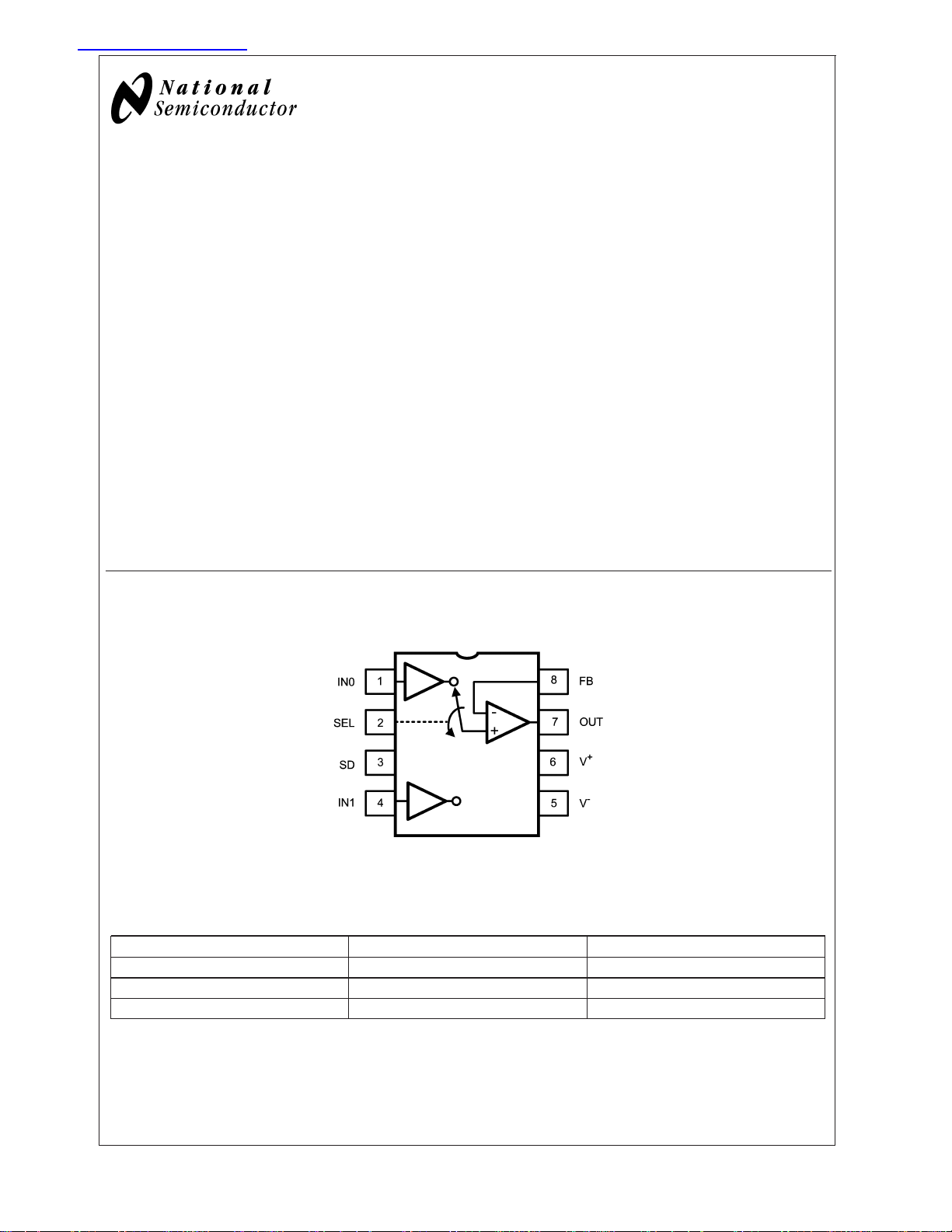
Connection Diagram
8-Pin SOIC
Features
n 500 MHz, 500 mVPP, −3 dB bandwidth, AV=2
n 400 MHz, 2V
n 8 ns channel switching time
n 70 dB channel to channel isolation
n 0.02%, 0.05˚ diff. gain, diff. phase
n 0.1 dB gain flatness to 150 MHz
n 2200 V/µs slew rate
n Wide supply voltage range: 6V (
n −68 dB HD2
n −84 dB HD3
, −3 dB bandwidth, AV=2
PP
±
@
5 MHz
@
5 MHz
@
10 MHz
3V) to 12V (±6V)
Applications
n Video router
n Multi input video monitor
n Instrumentation / Test equipment
n Receiver IF diversity switch
n Multi channel A/D driver
n Picture in Picture video switch
Top View
20129905
Truth Table
SEL SD OUTPUT
1 0 IN1 * (1+RF/RG)
0 0 IN0 * (1+RF/RG)
X 1 Shutdown
LMH™is a trademark of National Semiconductor Corporation.
© 2005 National Semiconductor Corporation DS201299 www.national.com
Absolute Maximum Ratings (Note 1)
If Military/Aerospace specified devices are required,
please contact the National Semiconductor Sales Office/
LMH6570
Distributors for availability and specifications.
Storage Temperature Range −65˚C to +150˚C
Soldering Information
Infrared or Convection (20 sec) 235 ˚C
Wave Soldering (10 sec) 260 ˚C
ESD Tolerance (Note 4)
Human Body Model 2000V
Operating Ratings (Note 1)
Machine Model 200V
+−V−
Supply Voltage (V
I
(Note 3) 130 mA
OUT
Signal & Logic Input Pin Voltage
Signal & Logic Input Pin Current
) 13.2V
±
(VS+0.6V)
±
20 mA
Maximum Junction Temperature +150˚C
±
5V Electrical Characteristics
Operating Temperature −40 ˚C to 85 ˚C
Supply Voltage Range 6V to 12V
Thermal Resistance
Package (θ
)(θJC)
JA
8-Pin SOIC 150˚C/W 50˚C/W
VS=±5V, RL= 100Ω,RF=576Ω,AV=2 V/V, TJ=25 ˚C, Unless otherwise specified. Bold numbers specify limits at temperature
extremes.
Symbol Parameter Conditions (Note 2) Min
(Note 5)
Typ
(Note 9)
Max
(Note 5)
Frequency Domain Performance
SSBW −3 dB Bandwidth V
LSBW –3 dB Bandwidth V
.1 dBBW 0.1 dB Bandwidth V
DG Differential Gain R
DP Differential Phase R
= 0.5 V
OUT
OUT
OUT
= 150Ω, f=4.43 MHz 0.02 %
L
= 150Ω, f=4.43 MHz 0.05 deg
L
=2V
PP
= 0.25 V
PP
PP
500 MHz
400 MHz
150 MHz
XTLK Channel to Channel Crosstalk All Hostile,f=5MHz −70 dBc
Time Domain Response
TRS Channel to Channel Switching Time Logic transition to 90% output 8 ns
Enable and Disable Times Logic transition to 90% or 10%
10 ns
output.
TRL Rise and Fall Time 4V Step 2.4 ns
TSS Settling Time to 0.05% 2V Step 17 ns
OS Overshoot 2V Step 5 %
SR Slew Rate 4V Step, (Note 8) 2200 V/µs
Distortion
HD2 2
HD3 3
IMD 3
nd
Harmonic Distortion 2 VPP, 5 MHz −68 dBc
rd
Harmonic Distortion 2 VPP, 5 MHz −84 dBc
rd
Order Intermodulation Products 10 MHz, Two tones 2 Vpp at output −80 dBc
Equivalent Input Noise
VN Voltage
ICN Current
>
1 MHz, Input Referred 5 nV
>
1 MHz, Input Referred 5 pA/
Static, DC Performance
CHGM Channel to Channel Gain Difference DC, Difference in gain between
channels
VIO Input Offset Voltage V
=0V 1
IN
±
0.005±0.034
±
0.036
±
±
15
21
DVIO Offset Voltage Drift (Note 10) 30 µV/˚C
IBN Input Bias Current (Note 7) V
=0V −3
IN
±
5.5
±
6.2
DIBN Bias Current Drift (Note 10) 11 nA/˚C
IBI Inverting Input Bias Current (Note 7) Pin 8, Feedback point,
V
=0V
IN
PSRR Power Supply Rejection Ratio DC, Input referred 48
−3
50 dB
±
18
±
22
46
Units
%
mV
µA
uA
www.national.com 2
±
5V Electrical Characteristics (Continued)
VS=±5V, RL= 100Ω,RF=576Ω,AV=2 V/V, TJ=25 ˚C, Unless otherwise specified. Bold numbers specify limits at temperature
extremes.
Symbol Parameter Conditions (Note 2) Min
(Note 5)
ICC Supply Current No Load, Shutdown Pin (SD)
0.8V
Supply Current Shutdown Shutdown Pin (SD)
VIH Logic High Threshold Select Pin & Shutdown pin (SEL,
SD)
VIL Logic Low Threshold Select Pin & Shutdown pin (SEL,
SD)
IiL Logic Pin Input Current Low (Note 7) Logic Input = 0V Select Pin &
Shutdown pin (SEL, SD)
IiH Logic Pin Input Current High (Note 7) Logic Input = 5.0V, Select Pin &
Shutdown pin (SEL, SD)
Miscellaneous Performance
RIN+ Input Resistance 5kΩ
CIN Input Capacitance 0.8 pF
ROUT Output Resistance Output Active, (SD
ROUT Output Resistance Output Disabled, (SD
COUT Output Capacitance Output Disabled, (SD
VO Output Voltage Range No Load
VOL R
CMIR Input Voltage Range
IO Linear Output Current (Note 7) V
ISC Short Circuit Current(Note 3) V
= 100Ω
L
= 0V, +60
IN
=±2V, Output shorted to
IN
ground
>
<
0.8V) 0.04 Ω
>
2V 1.1 1.3
2.0 V
−2.9
-10
>
2V) 3000 Ω
>
2V) 3.1 pF
±
3.51
±
3.50
±
3.16
±
3.15
±
2.5
-70
±
55
Typ
(Note 9)
13.8 15
−1 µA
57 68
±
3.7 V
±
3.5 V
±
2.6 V
±
80 mA
±
230 mA
Max
(Note 5)
16
1.4
0.8 V
75
Units
mA
mA
µA
LMH6570
±
3.3V Electrical Characteristics
VS=±3.3V, RL= 100Ω,RF=576Ω,AV=2 V/V; Unless otherwise specified.
Symbol Parameter Conditions (Note 2) Min
(Note 5)
Frequency Domain Performance
SSBW −3 dB Bandwidth V
LSBW −3 dB Bandwidth V
0.1 dBBW 0.1 dB Bandwidth V
GFP Peaking DC to 200 MHz 0.4 dB
XTLK Channel to Channel Crosstalk All Hostile,f=5MHz −70 dBc
Time Domain Response
TRL Rise and Fall Time 2V Step 2 ns
TSS Settling Time to 0.05% 2V Step 20 ns
OS Overshoot 2V Step 5 %
SR Slew Rate 2V Step 1400 V/µs
Distortion
HD2 2
HD3 3
Static, DC Performance
nd
Harmonic Distortion 2 VPP, 10 MHz −67 dBc
rd
Harmonic Distortion 2 VPP, 10 MHz −87 dBc
OUT
OUT
OUT
= 0.5 V
= 2.0 V
= 0.5 V
PP
PP
PP
Typ
(Note 9)
475 MHz
375 MHz
100 MHz
Max
(Note 5)
www.national.com3
Units
±
3.3V Electrical Characteristics (Continued)
VS=±3.3V, RL= 100Ω,RF=576Ω,AV=2 V/V; Unless otherwise specified.
LMH6570
Symbol Parameter Conditions (Note 2) Min
(Note 5)
VIO Input Offset Voltage V
IBN Input Bias Current (Note 7) V
=0V 1 mV
IN
=0V -3 µA
IN
Typ
(Note 9)
Max
(Note 5)
PSRR Power Supply Rejection Ratio DC, Input Referred 49 dB
ICC Supply Current No Load 12.5 mA
VIH Logic High Threshold Select Pin & Shutdown pin (SEL,
1.3 V
SD),
+
VIH )V
VIL Logic Low Threshold Select Pin & Shutdown pin (SEL,
* 0.4
0.4 V
SD),
+
VIL )V
* 0.12
Miscellaneous Performance
RIN+ Input Resistance 5kΩ
CIN Input Capacitance 0.8 pF
ROUT Output Resistance 0.06 Ω
VO Output Voltage Range No Load
VOL R
= 100Ω
L
CMIR Input Voltage Range
IO Linear Output Current (Note 3) V
ISC Short Circuit Current (Note 3) V
=0V
IN
=±1V, Output shorted to
IN
±
2V
±
1.8 V
±
1.2 V
±
60 mA
±
150 mA
ground
Note 1: Absolute Maximum Ratings indicate limits beyond which damage to the device may occur. Operating Ratings indicate conditions for which the device is
intended to be functional, but specific performance is not guaranteed. For guaranteed specifications, see the Electrical Characteristics tables.
Note 2: Electrical Table values apply only for factory testing conditions at the temperature indicated. Factory testing conditions result in very limited self-heating of
the device such that T
See Applications Section for information on temperature de-rating of this device. Min/Max ratings are based on product testing, characterization and simulation.
Individual parameters are tested as noted.
Note 3: The maximum output current (I
150˚C). See the Power Dissipation section of the Application Section for more details. A short circuit condition should be limited to 5 seconds or less.
Note 4: Human Body model, 1.5kΩ in series with 100pF. Machine model, 0Ω In series with 200pF
Note 5: Limits are 100% production tested at 25˚C. Limits over the operating temperature range are guaranteed through correlation using Statistical Quality Control
(SQC) methods.
Note 6: Parameter guaranteed by design.
Note 7: Positive Value is current into device.
Note 8: Slew Rate is the average of the rising and falling edges.
Note 9: Typical numbers are the most likely parametric norm.
Note 10: Drift determined by dividing the change in parameter at temperature extremes by the total temperature change.
. No guarantee of parametric performance is indicated in the electrical tables under conditions of internal self heating where T
J=TA
) is determined by the device power dissipation limitations (The junction temperature cannot be allowed to exceed
OUT
Units
>
TA.
J
Ordering Information
Package Part Number Package Marking Transport Media NSC Drawing
8-Pin SOIC
www.national.com 4
LMH6570MA
LMH6570MAX 2.5k Units Tape and Reel
LMH6570MA
95 Units/Rail
M08A
LMH6570
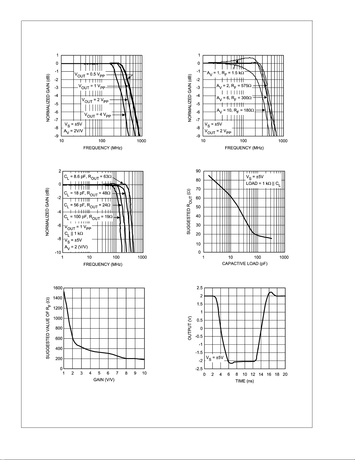
Typical Performance Characteristics V
specified.
Frequency Response vs. V
Frequency Response vs. Capacitive Load Suggested R
OUT
20129902 20129903
=±5V, RL= 100Ω,AV=2, RF=RG=576Ω; unless otherwise
s
Frequency Response vs. Gain
vs. Capacitive Load
OUT
20129914
Suggested Value of RFvs. Gain Pulse Response 4V
20129901
20129915
PP
20129925
www.national.com5

Typical Performance Characteristics V
specified. (Continued)
LMH6570
Pulse Response 2V
PP
Closed Loop Output Impedance Closed Loop Output Impedance
=±5V, RL= 100Ω,AV=2, RF=RG=576Ω; unless otherwise
s
Pulse Response 2V
20129929 20129930
PP
20129908
PSRR vs. Frequency Channel Switching
20129904 20129916
www.national.com 6
20129909

LMH6570
Typical Performance Characteristics V
specified. (Continued)
SHUTDOWN Switching Shutdown Glitch
20129921
HD2 vs. Frequency HD3 vs. Frequency
=±5V, RL= 100Ω,AV=2, RF=RG=576Ω; unless otherwise
s
20129927
HD2 vs. V
20129933
S
20129907 20129910
HD3 vs. V
S
20129934
www.national.com7

Typical Performance Characteristics V
specified. (Continued)
LMH6570
Minimum V
HD2 vs. V
vs. I
OUT
OUT
20129911 20129906
(Note 7) Maximum V
OUT
=±5V, RL= 100Ω,AV=2, RF=RG=576Ω; unless otherwise
s
HD3 vs. V
OUT
vs. I
OUT
OUT
(Note 7)
20129912 20129913
Crosstalk vs. Frequency Off Isolation
20129935
www.national.com 8
20129931

Application Notes
GENERAL INFORMATION
LMH6570
FIGURE 1. Typical Application
The LMH6570 is a high-speed 2:1 analog multiplexer, optimized for very high speed and low distortion. With selectable
gain and excellent AC performance, the LMH6570 is ideally
suited for switching high resolution, presentation grade video
signals. The LMH6570 has no internal ground reference.
Single or split supply configurations are both possible, however, all logic functions are referenced to the mid supply
point. The LMH6570 features very high speed channel
switching and disable times. When disabled the LMH6570
output is high impedance making MUX expansion possible
by combining multiple devices. See “Multiplexer Expansion”
section below. The LMH6570 SEL defaults to logic low (IN0
active). The default state for the SD pin is also logic low
(device enabled). Both pins can be left floating if the default
state is desired.
VIDEO PERFORMANCE
The LMH6570 has been designed to provide excellent performance with production quality video signals in a wide
variety of formats such as HDTV and High Resolution VGA.
Best performance will be obtained with back-terminated
loads. The back termination reduces reflections from the
transmission line and effectively masks transmission line
and other parasitic capacitances from the amplifier output
stage. Figure 1 shows a typical configuration for driving a
75Ω cable. The output buffer is configured for a gain of 2, so
using back terminated loads will give a net gain of 1.
20129922
FEEDBACK RESISTOR SELECTION
20129932
FIGURE 2. Suggested RFvs. Gain
The LMH6570 has a current feedback output buffer with gain
determined by external feedback (R
) and gain set (RG)
F
resistors. With current feedback amplifiers, the closed loop
frequency response is a function of R
the recommended value of R
the chart “Suggested R
is 576Ω. For other gains see
F
vs Gain”. Generally, lowering R
F
. For a gain of 2 V/V,
F
from the recommended value will peak the frequency re-
F
www.national.com9

Application Notes (Continued)
sponse and extend the bandwidth while increasing the value
LMH6570
of R
will cause the frequency response to roll off faster.
F
Reducing the value of R
value will cause overshoot, ringing and, eventually, oscillation.
Since all applications are slightly different it is worth some
experimentation to find the optimal R
more information see Application Note OA-13 which describes the relationship between R
quency response for current feedback operational amplifiers.
The impedance looking into pin 8 is approximately 20Ω. This
allows for good bandwidth at gains up to 10 V/V. When used
with gains over 10 V/V, the LMH6570 will exhibit a “gain
bandwidth product” similar to a typical voltage feedback
amplifier. For gains of over 10 V/V consider selecting a high
performance video amplifier like the LMH6720 to provide
additional gain.
EVALUATION BOARDS
National Semiconductor provides the following evaluation
boards as a guide for high frequency layout and as an aid in
device testing and characterization. Many of the data sheet
plots were measured with this board.
Device Package Evaluation Board
LMH6570 SOIC LMH730277
too far below the recommended
F
for a given circuit. For
F
and closed-loop fre-
F
loading effect on the active output caused by the unselected
devices. The circuit in Figure 3 shows how to compensate
for this effect. For the 8:1 MUX function shown in Figure 3
below the gain error would be about 0.7% or −0.06dB. In the
circuit in Figure 3, resistor ratios have been adjusted to
compensate for this gain error. By adjusting the gain of each
multiplexer circuit the error can be reduced to the tolerance
of the resistors used (1% in this example).
20129917
FIGURE 3. Multiplexer Gain Compensation
An evaluation board can be shipped when a sample request
is placed with National Semiconductor. Samples can be
ordered on the National web page. (www.national.com)
MULTIPLEXER EXPANSION
With the SHUTDOWN pin putting the output stage into a
high impedance state, several LMH6570’s can be tied together to form a larger input MUX. However, there is a
BUILDING A 4:1 MULITPLEXER
Figure 4 shows an 4:1 MUX using two LMH6570’s.
www.national.com 10

Application Notes (Continued)
LMH6570
FIGURE 4. 4:1 MUX USING TWO LMH6570’s
20129919
FIGURE 5. Delay Circuit Implementation
If it is important in the end application to make sure that no
two inputs are presented to the output at the same time, an
optional delay block can be added, to drive the SHUTDOWN
pin of each device, as shown. Figure 5 shows one possible
approach to this delay circuit. The delay circuit shown will
delay SHUTDOWN’s H to L transitions (R
and C1decay)
1
20129918
but won’t delay its L to H transition. R
compared to R
in order to not reduce the SHUTDOWN
1
should be kept small
2
voltage and to produce little or no delay to SHUTDOWN.
Other Applications
The LMH6570 could support a dual antenna receiver with
two physically separate antennas. Monitoring the signal
strength of the active antenna and switching to the other
antenna when a fade is detected is a simple way to achieve
spacial diversity. This method gives about a 3dB boost in
average signal strength and is the least expensive method
for combining signals.
DRIVING CAPACITIVE LOADS
Capacitive output loading applications will benefit from the
use of a series output resistor R
of a series output resistor, R
output under capacitive loading. Capacitive loads of
. Figure 6 shows the use
OUT
, to stabilize the amplifier
OUT
www.national.com11

Other Applications (Continued)
5 to 120 pF are the most critical, causing ringing, frequency
LMH6570
response peaking and possible oscillation. The chart “Suggested R
selecting a series output resistor for mitigating capacitive
loads. The values suggested in the charts are selected for
0.5 dB or less of peaking in the frequency response. This
gives a good compromise between settling time and bandwidth. For applications where maximum frequency response
is needed and some peaking is tolerable, the value of R
can be reduced slightly from the recommended values.
vs. Cap Load” gives a recommended value for
OUT
OUT
20129914
FIGURE 8. Frequency Response vs. Capacitive Load
FIGURE 6. Decoupling Capacitive Loads
FIGURE 7. Suggested R
vs. Capacitive Load
OUT
20129924
20129915
LAYOUT CONSIDERATIONS
Whenever questions about layout arise, use the evaluation
board as a guide. The LMH730277 is the evaluation board
supplied with samples of the LMH6570. To reduce parasitic
capacitances, ground and power planes should be removed
near the input and output pins. For long signal paths controlled impedance lines should be used, along with impedance matching elements at both ends. Bypass capacitors
should be placed as close to the device as possible. Bypass
capacitors from each rail to ground are applied in pairs. The
larger electrolytic bypass capacitors can be located farther
from the device, the smaller ceramic capacitors should be
placed as close to the device as possible. In Figure 1, the
capacitor between V
+
and V−is optional, but is recommended for best second harmonic distortion. Another way to
enhance performance is to use pairs of 0.01µF and 0.1µF
ceramic capacitors for each supply bypass.
POWER DISSIPATION
The LMH6570 is optimized for maximum speed and performance in the small form factor of the standard SOIC package. To ensure maximum output drive and highest performance, thermal shutdown is not provided. Therefore, it is of
utmost importance to make sure that the T
JMAX
is never
exceeded due to the overall power dissipation.
Follow these steps to determine the maximum power dissi-
pation for the LMH6570:
1. Calculate the quiescent (no-load) power: P
), where VS=V+-V−.
(V
S
AMP=ICC
2. Calculate the RMS power dissipated in the output stage:
(rms) = rms ((VS-V
P
D
are the voltage across and the current through the
I
OUT
external load and V
S
3. Calculate the total RMS power: P
)*I
OUT
), where V
OUT
is the total supply voltage.
T=PAMP+PD
OUT
and
.
The maximum power that t-he LMH6570 package can dissipate at a given temperature can be derived with the following
equation:
= (150˚ – T
P
MAX
ture (˚C) and θ
)/ θJA, where T
AMB
= Thermal resistance, from junction to
JA
= Ambient tempera-
AMB
ambient, for a given package (˚C/W). For the SOIC package
is 150 ˚C/W.
θ
JA
*
www.national.com 12

Other Applications (Continued)
ESD PROTECTION
The LMH6570 is protected against electrostatic discharge
(ESD) on all pins. The LMH6570 will survive 2000V Human
Body model and 200V Machine model events. Under normal
operation the ESD diodes have no effect on circuit performance. There are occasions, however, when the ESD di-
LMH6570
odes will be evident. If the LMH6570 is driven by a large
signal while the device is powered down the ESD diodes will
conduct . The current that flows through the ESD diodes will
either exit the chip through the supply pins or will flow
through the device, hence it is possible to power up a chip
with a large signal applied to the input pins. Using the
shutdown mode is one way to conserve power and still
prevent unexpected operation.
www.national.com13

Physical Dimensions inches (millimeters) unless otherwise noted
LMH6570 2:1 High Speed Video Multiplexer
8-Pin SOIC
NS Package Number M08A
National does not assume any responsibility for use of any circuitry described, no circuit patent licenses are implied and National reserves
the right at any time without notice to change said circuitry and specifications.
For the most current product information visit us at www.national.com.
LIFE SUPPORT POLICY
NATIONAL’S PRODUCTS ARE NOT AUTHORIZED FOR USE AS CRITICAL COMPONENTS IN LIFE SUPPORT DEVICES OR SYSTEMS
WITHOUT THE EXPRESS WRITTEN APPROVAL OF THE PRESIDENT AND GENERAL COUNSEL OF NATIONAL SEMICONDUCTOR
CORPORATION. As used herein:
1. Life support devices or systems are devices or systems
which, (a) are intended for surgical implant into the body, or
(b) support or sustain life, and whose failure to perform when
properly used in accordance with instructions for use
2. A critical component is any component of a life support
device or system whose failure to perform can be reasonably
expected to cause the failure of the life support device or
system, or to affect its safety or effectiveness.
provided in the labeling, can be reasonably expected to result
in a significant injury to the user.
BANNED SUBSTANCE COMPLIANCE
National Semiconductor manufactures products and uses packing materials that meet the provisions of the Customer Products
Stewardship Specification (CSP-9-111C2) and the Banned Substances and Materials of Interest Specification (CSP-9-111S2) and contain
no ‘‘Banned Substances’’ as defined in CSP-9-111S2.
National Semiconductor
Americas Customer
Support Center
Email: new.feedback@nsc.com
Tel: 1-800-272-9959
www.national.com
National Semiconductor
Europe Customer Support Center
Fax: +49 (0) 180-530 85 86
Email: europe.support@nsc.com
Deutsch Tel: +49 (0) 69 9508 6208
English Tel: +44 (0) 870 24 0 2171
Français Tel: +33 (0) 1 41 91 8790
National Semiconductor
Asia Pacific Customer
Support Center
Email: ap.support@nsc.com
National Semiconductor
Japan Customer Support Center
Fax: 81-3-5639-7507
Email: jpn.feedback@nsc.com
Tel: 81-3-5639-7560
 Loading...