

National Semiconductor LMH6560 Technical data

查询LMH6560供应商
LMH6560
Quad, High-Speed, Closed-Loop Buffer
LMH6560 Quad, High-Speed, Closed-Loop Buffer
April 2003
General Description
The LMH6560 is a high speed, closed-loop buffer designed
for applications requiring the processing of very high frequency signals. While offering a small signal bandwidth of
680MHz, and a very high slew rate of 3100V/µs the
LMH6560 consumes only 46mA of quiescent current for all
four buffers. Total harmonic distortion into a load of 100Ω at
20MHz is −51dBc. The LMH6560 is configured internally for
a loop gain of one. Input resistance is 100kΩ and output
resistance is but 1.5Ω. Crosstalk between the buffers is only
−55dB. These characteristics make the LMH6560 an ideal
choice for the distribution of high frequency signals on
printed circuit boards. Differential gain and phase specifications of 0.10% and 0.03˚ respectively at 3.58MHz make the
LMH6560 well suited for the buffering of video signals.
The device is fabricated on National’s high speed VIP10
process using National’s proven high performance circuit
architectures.
Typical Schematic
Features
n Closed-loop quad buffer
n 680MHz small signal bandwidth
n 3100V/µs slew rate
n 0.10% / 0.03˚ differential gain / phase
n −51dBc THD at 20MHz
n Single supply operation (3V min.)
n 80mA output current
Applications
n Multi-channel video distribution
n Video switching and routing
n High-speed analog multiplexing
n Channelized EW
n High-density buffering
n Active filters
n Broadcast and high definition TV systems
n Medical imaging
n Test equipment and instrumentation
20064235
© 2003 National Semiconductor Corporation DS200642 www.national.com
Absolute Maximum Ratings (Note 1)
If Military/Aerospace specified devices are required,
please contact the National Semiconductor Sales Office/
LMH6560
Distributors for availability and specifications.
ESD Tolerance
Human Body Model 2000V (Note 2)
Machine Model 200V (Note 3)
Output Short Circuit Duration (Note 4),(Note 5)
Supply Voltage (V
Voltage at Input/Output Pins V
Soldering Information
Infrared or Convection (20 sec.) 235˚C
±
5V Electrical Characteristics
+–V−
) 13V
+
+0.8V, V−−0.8V
Wave Soldering (10 sec.) 260˚C
Storage Temperature Range −65˚C to +150˚C
Junction Temperature (Note 6) +150˚C
Operating Ratings (Note 1)
Supply Voltage (V
Operating Temperature Range
(Note 6), (Note 7)
Package Thermal Resistance (Note 6), (Note 7)
14-Pin SOIC 137˚C/W
14-Pin TSSOP 160˚C/W
+–V−
) 3-10V
−40˚C to +85˚C
Unless otherwise specified, all limits guaranteed for TJ= 25˚C, V+= +5V, V−= −5V, VO=VCM= 0V and RL= 100Ω to 0V.
Boldface limits apply at the temperature extremes.
Symbol Parameter Conditions
Min
(Note 9)
Typ
(Note 8)
Max
(Note 9) Units
Frequency Domain Response
SSBW Small Signal Bandwidth V
GFN Gain Flatness
<
0.1dB V
FPBW Full Power Bandwidth (−3dB) V
DG Differential Gain R
0.5V
O
O
O
L
PP
<
0.5V
PP
=2VPP(+10dBm) 280 MHZ
= 150Ω to 0V;
680 MHz
375 MHz
0.10 %
<
f = 3.58MHz
DP Differential Phase R
= 150Ω to 0V;
L
0.03 deg
f = 3.58MHz
Time Domain Response
t
r
t
f
t
s
Rise Time 3.3V Step (20-80%) 0.6 ns
Fall Time 0.7 ns
Settling Time to 0.1% 3.3V Step 9 ns
OS Overshoot 1V Step 4 %
SR Slew Rate (Note 11) 3100 V/µs
Distortion And Noise Performance
HD2 2
HD3 3
THD Total Harmonic Distortion V
e
n
nd
Harmonic Distortion VO=2VPP; f = 20MHz −58 dBc
rd
Harmonic Distortion VO=2VPP; f = 20MHz −52 dBc
=2VPP; f = 20MHz −51 dBc
O
Input-Referred Voltage Noise f = 1MHz 3 nV/
CP 1dB Compression Point f = 10MHz +23 dBm
CT Amplifier Crosstalk Receiving Amplifier:
=50Ω to 0V; f = 10MHz
R
S
SNR Signal to Noise Ratio f = 5MHz; V
AGM Amplifier Gain Matching R
=2kΩ to 0V; f = 5MHz;
L
=1V
V
O
=1V
O
PP
PP
−55 dB
120 dB
0.05 dB
Static, DC Performance
A
CL
Small Signal Voltage Gain VO= 100mV
PP
0.97 0.995
RL= 100Ω to 0V
V
O
= 100mV
PP
0.99 0.998
RL=2kΩ to 0V
V
OS
Input Offset Voltage 2 20
25
TC V
Temperature Coefficient Input
OS
(Note 12) 28 µV/˚C
Offset Voltage
V/V
mV
www.national.com 2

±
5V Electrical Characteristics (Continued)
Unless otherwise specified, all limits guaranteed for TJ= 25˚C, V+= +5V, V−= −5V, VO=VCM= 0V and RL= 100Ω to 0V.
Boldface limits apply at the temperature extremes.
Symbol Parameter Conditions
I
B
Input Bias Current (Note 10) −10
Min
(Note 9)
Typ
(Note 8)
Max
(Note 9) Units
−5 µA
−14
TC I
Temperature Coefficient Input
B
(Note 12) −4.7 nA/˚C
Bias Current
R
OUT
PSRR Power Supply Rejection Ratio V
I
S
Output Resistance RL= 100Ω to 0V; f = 100kHz 1.5
R
= 100Ω to 0V; f = 10MHz 1.6
L
=±5V to VS=±5.25V;
S
=0V
V
IN
48
44
67 dB
Supply Current, All 4 Buffers No Load 46 58
63
Miscellaneous Performance
R
IN
C
IN
V
O
Input Resistance 100 kΩ
Input Capacitance 2 pF
Output Swing Positive RL= 100Ω to 0V 3.10
3.34
3.08
=2kΩ to 0V 3.58
R
L
3.64
3.55
Output Swing Negative RL= 100Ω to 0V −3.34 −3.20
−3.17
=2kΩ to 0V −3.64 −3.58
R
L
−3.55
I
SC
I
O
Output Short Circuit Current Sourcing: VIN=V+;VO= 0V −83
Sinking: V
Linear Output Current Sourcing: VIN-VO= 0.5V
(Note 10)
Sinking: V
(Note 10)
=V−;VO=0V 83
IN
−50
−42
IN-VO
= −0.5V
50
40
−74
74
LMH6560
Ω
mA
V
V
mA
mA
5V Electrical Characteristics
Unless otherwise specified, all limits guaranteed for TJ= 25˚C, V+= +5V, V−= 0V, VO=VCM=V+/2 and RL= 100Ω to V+/2.
Boldface limits apply at the temperature extremes.
Min
Symbol Parameter Conditions
(Note 9)
Frequency Domain Response
<
SSBW Small Signal Bandwidth V
GFN Gain Flatness
<
0.1dB V
FPBW Full Power Bandwidth (−3dB) V
DG Differential Gain R
0.5V
O
O
O
L
PP
<
0.5V
PP
=2VPP(+10dBm) 175 MHZ
= 150Ω to V+/2;
f = 3.58MHz
DP Differential Phase RL= 150Ω to V+/2;
f = 3.58MHz
Time Domain Response
t
r
t
f
t
s
Rise Time 2.3VPPStep (20-80%) 0.8 ns
Fall Time 1.0 ns
Settling Time to 0.1% 2.3V Step 10 ns
OS Overshoot 1V Step 0 %
SR Slew Rate (Note 11) 1445 V/µs
Typ
(Note 8)
Max
(Note 9) Units
455 MHz
75 MHz
0.4 %
0.09 deg
www.national.com3
5V Electrical Characteristics (Continued)
Unless otherwise specified, all limits guaranteed for TJ= 25˚C, V+= +5V, V−= 0V, VO=VCM=V+/2 and RL= 100Ω to V+/2.
Boldface limits apply at the temperature extremes.
LMH6560
Min
Symbol Parameter Conditions
(Note 9)
Distortion And Noise Performance
nd
HD2 2
HD3 3
THD Total Harmonic Distortion V
e
n
Harmonic Distortion VO=2VPP; f = 20MHz −52 dBc
rd
Harmonic Distortion VO=2VPP; f = 20MHz −54 dBc
=2VPP; f = 20MHz −50 dBc
O
Input-Referred Voltage Noise f = 1MHz 3 nV/
CP 1dB Compression Point f = 10MHz +14 dBm
CT Amplifier Crosstalk Receiving Amplifier:
=50Ω to V+/2; f = 10MHz
R
S
SNR Signal to Noise Ratio V
AGM Amplifier Gain Matching V
=1VPP; f = 5MHz 120 dB
O
=1V
O
PP
RL=2kΩ to V+/2; f = 5MHz
Static, DC Performance
A
CL
Small Signal Voltage Gain VO= 100mV
PP
0.97 0.994
RL= 100Ω to V+/2
V
O
= 100mV
PP
0.99 0.998
RL=2kΩ to V+/2
V
OS
TC V
Input Offset Voltage 2 13
Temperature Coefficient Input
OS
(Note 12) 2 µV/˚C
Offset Voltage
I
B
Input Bias Current (Note 10) −5
−5.5
TC I
Temperature Coefficient Input
B
(Note 12) 1.3 nA/˚C
Bias Current
R
OUT
PSRR Power Supply Rejection Ratio V
I
S
Output Resistance RL= 100Ω to V+/2; f = 100kHz 1.7
R
= 100Ω to V+/2; f = 10MHz 2.0
L
= +5V to VS= +5.5V;
S
IN=VS
/2
V
48
45
Supply Current All 4 Buffer No Load 21 26
Miscellaneous Performance
R
IN
C
IN
V
O
Input Resistance 16 kΩ
Input Capacitance 2 pF
Output Swing Positive RL= 100Ω to V+/2 3.74
3.70
RL=2kΩ to V+/2 3.92
3.90
Output Swing Negative R
I
SC
I
O
Output Short Circuit Current Sourcing: VIN=V+;VO=V+/2 −40
Linear Output Current Sourcing: VIN-VO= 0.5V
= 100Ω to V+/2 1.15 1.22
L
=2kΩ to V+/2 1.04 1.08
R
L
Sinking: V
=V−;VO=V+/2 22
IN
−50
(Note 10)
Sinking: VIN-VO= −0.5V
(Note 10)
−40
30
20
Typ
(Note 8)
Max
(Note 9) Units
−55 dB
0.5 dB
15
−2.5 µA
67 dB
30
3.85
3.96
1.27
1.10
−64
45
V/V
mV
Ω
mA
V
V
mA
mA
www.national.com 4
3V Electrical Characteristics
Unless otherwise specified, all limits guaranteed for TJ= 25˚C, V+= 3V, V−= 0V, VO=VCM=V+/2 and RL= 100Ω to V+/2.
Boldface limits apply at the temperature extremes.
Min
Symbol Parameter Conditions
(Note 9)
Frequency Domain Response
<
SSBW Small Signal Bandwidth V
GFN Gain Flatness
<
0.1dB V
FPBW Full Power Bandwidth (−3dB) V
0.5V
O
O
O
PP
<
0.5V
PP
=1VPP(+4.5dBm) 115 MHZ
Time Domain Response
t
r
t
f
t
s
Rise Time 1V Step (20-80%) 1.1 ns
Fall Time 1.3 ns
Settling Time to 0.1% 1V Step 11 ns
OS Overshoot 0.5V Step 0 %
SR Slew Rate (Note 11) 480 V/µs
Distortion And Noise Performance
HD2 2
HD3 3
THD Total Harmonic Distortion V
e
n
nd
Harmonic Distortion VO= 0.5VPP; f = 20MHz −55 dBc
rd
Harmonic Distortion VO= 0.5VPP; f = 20MHz −61 dBc
= 0.5VPP; f = 20MHz −54 dBc
O
Input-Referred Voltage Noise f = 1MHz 3 nV/
CP 1dB Compression Point f = 10MHz +4 dBm
CT Amplifier Crosstalk Receiving Amplifier:
=50Ω to V+/2; f = 10MHz
R
S
SNR Signal to Noise Ratio f = 5MHz; V
AGM Amplifier Gain Matching R
=2kΩ to V+/2;
L
f = 5MHz; V
O
O
=1V
=1V
PP
PP
Static, DC Performance
A
CL
Small Signal Voltage Gain VO= 100mV
PP
0.97 0.99
RL= 100Ω to V+/2
V
O
= 100mV
PP
0.99 0.997
RL=2kΩ to V+/2
V
OS
TC V
Input Offset Voltage 1.6 8
Temperature Coefficient Input
OS
(Note 12) 2.6 µV/˚C
Offset Voltage
I
B
Input Bias Current (Note 10) −3
−3.5
TC I
Temperature Coefficient Input
B
(Note 12) 0.3 nA/˚C
Bias Current
R
OUT
PSRR Power Supply Rejection Ratio V
I
S
Output Resistance RL= 100Ω to V+/2; f = 100kHz 2.1
R
= 100Ω to V+/2; f = 10MHz 2.8
L
= +3V to VS= +3.5V;
S
IN=VS
/2
V
48
46
Supply Current, All 4 Buffers No Load 11 15
Miscellaneous Performance
R
IN
C
IN
Input Resistance 17 kΩ
Input Capacitance 2 pF
Typ
(Note 8)
Max
(Note 9) Units
265 MHz
40 MHz
−55 dB
120 dB
0.4 dB
10
−1.4 µA
65 dB
18
V/V
mV
Ω
mA
LMH6560
www.national.com5
3V Electrical Characteristics (Continued)
Unless otherwise specified, all limits guaranteed for TJ= 25˚C, V+= 3V, V−= 0V, VO=VCM=V+/2 and RL= 100Ω to V+/2.
Boldface limits apply at the temperature extremes.
LMH6560
Min
Symbol Parameter Conditions
V
O
Output Swing Positive RL= 100Ω to V+/2 2.0
(Note 9)
1.93
RL=2kΩ to V+/2 2.1
2.0
Output Swing Negative R
= 100Ω to V+/2 0.95 1.0
L
RL=2kΩ to V+/2 0.85 0.90
I
SC
I
O
Note 1: Absolute Maximum Ratings indicate limits beyond which damage to the device may occur. Operating Ratings indicate conditions for which the device is
intended to be functional, but specific performance is not guaranteed. For guaranteed specifications and the test conditions, see the Electrical Characteristics.
Note 2: Human body model, 1.5kΩ in series with 100pF
Note 3: Machine Model, 0Ω in series with 200pF.
Note 4: Applies to both single-supply and split-supply operation. Continuous short circuit operation at elevated ambient temperature can result in exceeding the
maximum allowed junction temperature of 150˚C.
Note 5: Short circuit test is a momentary test. See next note.
Note 6: The maximum power dissipation is a function of T
(T
J(MAX)-TA
Note 7: Electrical Table values apply only for factory testing conditions at the temperature indicated. Factory testing conditions result in very limited self-heating of
the device such that T
T
J
Note 8: Typical Values represent the most likely parametric norm.
Note 9: All limits are guaranteed by testing or statistical analysis.
Note 10: Positive current corresponds to current flowing into the device.
Note 11: Slew rate is the average of the positive and negative slew rate. Average Temperature Coefficient is determined by dividing the change in a parameter at
temperature extremes by the total temperature change.
Note 12: Average Temperature Coefficient is determined by dividing the change in a parameter at temperature extremes by the total temperature change.
Output Short Circuit Current Sourcing: VIN=V+;VO=V+/2 −26
Sinking: V
=V−;VO=V+/2 14
IN
Linear Output Current Sourcing: VIN-VO= 0.5V
(Note 10)
Sinking: V
IN-VO
= −0.5V
(Note 10)
, θJA, and TA. The maximum allowable power dissipation at any ambient temperature is PD=
)/θJA. All numbers apply for packages soldered directly onto a PC board.
. There is no guarantee of parametric performance as indicated in the electrical tables under conditions of internal self-heating where
>
TA. See Applications section for information on temperature de-rating of this device.
J=TA
J(MAX)
−20
−13
12
8
Typ
(Note 8)
2.05
2.15
−30
20
Max
(Note 9) Units
1.07
1.0
V
V
mA
mA
www.national.com 6
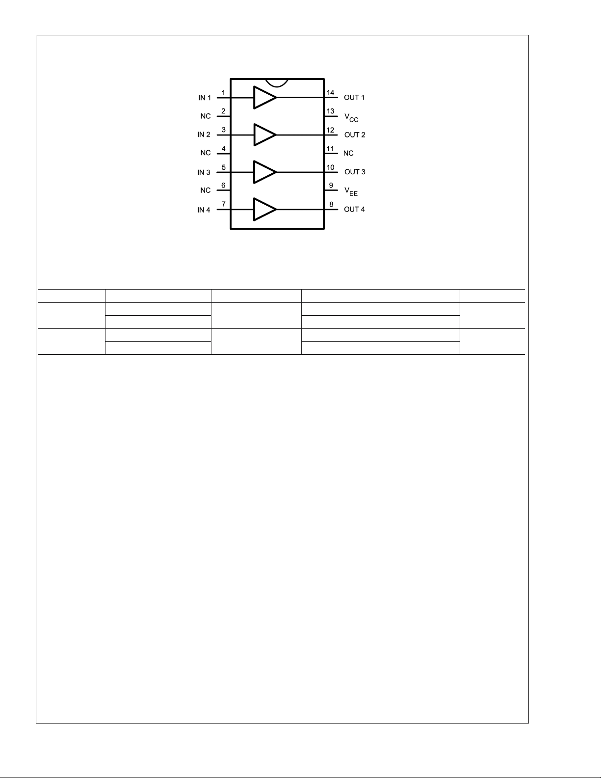
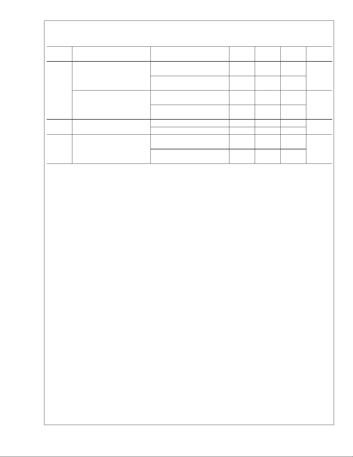
Connection Diagram
LMH6560
14-Pin SOIC/TSSOP
Top View
20064234
Ordering Information
Package Part Number Package Marking Transport Media NSC Drawing
14-pin SOIC LMH6560MA LMH6560MA 55 Units/Rail M14A
LMH6560MAX 2.5k Units Tape and Reel
14-pin TSSOP LMH6560MT LMH6560MT 94 Units/Rail MTC14
LMH6560MTX 2.5k Units Tape and Reel
www.national.com7
 Loading...