

查询LMH6559供应商
LMH6559
High-Speed, Closed-Loop Buffer
LMH6559 High-Speed, Closed-Loop Buffer
April 2003
General Description
The LMH6559 is a high-speed, closed-loop buffer designed
for applications requiring the processing of very high frequency signals. While offering a small signal bandwidth of
1750MHz, and an ultra high slew rate of 4580V/µs the
LMH6559 consumes only 10mA of quiescent current. Total
harmonic distortion into a load of 100Ω at 20MHz is −52dBc.
The LMH6559 is configured internally for a loop gain of one.
Input resistance is 200kΩ and output resistance is but 1.2Ω.
These characteristics make the LMH6559 an ideal choice for
the distribution of high frequency signals on printed circuit
boards. Differential gain and phase specifications of 0.06%
and 0.02˚ respectively at 3.58MHz make the LMH6559 well
suited for the buffering of video signals.
The device is fabricated on National’s high-speed VIP10
process using National’s proven high performance circuit
architectures.
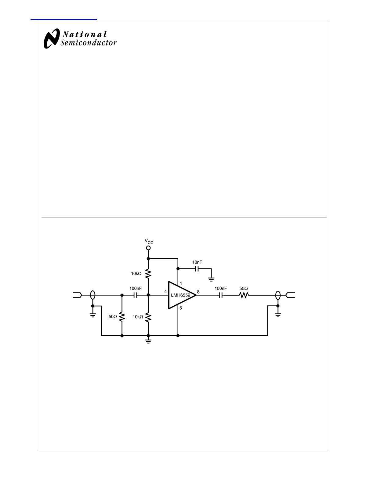
Typical Schematic
Features
n Closed-loop buffer
n 1750MHz small signal bandwidth
n 4580V/µs slew rate
n 0.06% / 0.02˚ differential gain/phase
n −52dBc THD at 20MHz
n Single supply operation (3V min.)
n 75mA output current
Applications
n Video switching and routing
n Test point drivers
n High frequency active filters
n Wideband DC clamping buffers
n High-speed peak detector circuits
n Transmission systems
n Telecommunications
n Test equipment and instrumentation
20064133
© 2003 National Semiconductor Corporation DS200641 www.national.com
Absolute Maximum Ratings (Note 1)
If Military/Aerospace specified devices are required,
please contact the National Semiconductor Sales Office/
LMH6559
Distributors for availability and specifications.
ESD Tolerance
Human Body Model 2000V (Note 2)
Machine Model 200V (Note 3)
Output Short Circuit Duration (Note 4), (Note 5)
Supply Voltage (V
Voltage at Input/Output Pins V
Soldering Information
Infrared or Convection (20 sec.) 235˚C
±
5V Electrical Characteristics
+–V−
) 13V
+
+0.8V, V−−0.8V
Wave Soldering (10 sec.) 260˚C
Storage Temperature Range −65˚C to +150˚C
Junction Temperature +150˚C
Operating Ratings (Note 1)
Supply Voltage (V
Operating Temperature
Range (Note 6), (Note 7) −40˚C to +85˚C
Package Thermal Resistance (Note 6), (Note 7)
8-Pin SOIC 172˚C/W
5-Pin SOT23 235˚C/W
+-V−
) 3 - 10V
Unless otherwise specified, all limits guaranteed for TJ= 25˚C, V+= +5V, V−= −5V, VO=VCM= 0V and RL= 100Ω to 0V.
Boldface limits apply at the temperature extremes.
Symbol Parameter Conditions
Min
(Note 9)
Typ
(Note 8)
Max
(Note 9) Units
Frequency Domain Response
SSBW Small Signal Bandwidth V
GFN Gain Flatness
<
0.1dB V
FPBW Full Power Bandwidth (−3dB) V
DG Differential Gain R
0.5V
O
O
O
L
PP
<
0.5V
PP
=2VPP(+10dBm) 1050 MHZ
= 150Ω to 0V;
1750 MHz
200 MHz
0.06 %
<
f = 3.58 MHz
DP Differential Phase R
= 150Ω to 0V;
L
0.02 deg
f = 3.58 MHz
Time Domain Response
t
r
t
f
t
s
Rise Time 3.3V Step (20-80%) 0.4 ns
Fall Time 0.5 ns
Settling Time to±0.1% 3.3V Step 9 ns
OS Overshoot 1V Step 4 %
SR Slew Rate (Note 11) 4580 V/µs
Distortion And Noise Performance
HD2 2
HD3 3
THD Total Harmonic Distortion V
e
n
nd
Harmonic Distortion VO=2VPP; f = 20MHz −58 dBc
rd
Harmonic Distortion VO=2VPP; f = 20MHz −53 dBc
=2VPP; f = 20MHz −52 dBc
O
Input-Referred Voltage Noise f = 1MHz 2.8 nV/
CP 1dB Compression point f = 10MHz +23 dBm
SNR Signal to Noise Ratio f = 5MHz; V
O
=1V
PP
120 dB
Static, DC Performance
A
CL
Small Signal Voltage Gain VO= 100mV
PP
.97 .996
RL= 100Ω to 0V
V
O
= 100mV
PP
.99 .998
RL=2kΩ to 0V
V
OS
Input Offset Voltage 3 20
25
TC V
Temperature Coefficient Input
OS
(Note 12) 23 µV/˚C
Offset Voltage
I
B
Input Bias Current (Note 10) −10
−3 µA
−14
TC I
Temperature Coefficient Input
B
(Note 12) −3.6 nA/˚C
Bias Current
V/V
mV
www.national.com 2

±
5V Electrical Characteristics (Continued)
Unless otherwise specified, all limits guaranteed for TJ= 25˚C, V+= +5V, V−= −5V, VO=VCM= 0V and RL= 100Ω to 0V.
Boldface limits apply at the temperature extremes.
Symbol Parameter Conditions
R
OUT
PSRR Power Supply Rejection Ratio V
Output Resistance RL= 100Ω to 0V; f = 100kHz 1.2
R
= 100Ω to 0V; f = 10MHz 1.3
L
=±5V to VS=±5.25V 48
S
Min
(Note 9)
Typ
(Note 8)
Max
(Note 9) Units
63 dB
44
I
S
Supply Current No Load 10 14
17
Miscellaneous Performance
R
IN
C
IN
V
O
Input Resistance 200 kΩ
Input Capacitance 1.7 pF
Output Swing Positive RL= 100Ω to 0V 3.20
3.45
3.18
RL=2kΩ to 0V 3.55
3.65
3.54
Output Swing Negative R
= 100Ω to 0V −3.45 −3.20
L
−3.18
=2kΩ to 0V −3.65 −3.55
R
L
−3.54
I
SC
I
O
Output Short Circuit Current Sourcing: VIN=+VS;VO= 0V −83
Sinking: V
Linear Output Current Sourcing: VIN-VO= 0.5V
(Note 10)
Sinking: V
(Note 10)
=−VS;VO=0V 83
IN
−50
−43
IN-VO
= −0.5V
50
43
−74
74
LMH6559
Ω
mA
V
V
mA
mA
5V Electrical Characteristics
Unless otherwise specified, all limits guaranteed for TJ= 25˚C, V+= 5V, V−= 0V, VO=VCM=V+/2 and RL= 100Ω to V+/2.
Boldface limits apply at the temperature extremes.
Min
Symbol Parameter Conditions
(Note 9)
Frequency Domain Response
<
SSBW Small Signal Bandwidth V
GFN Gain Flatness
<
0.1dB V
FPBW Full Power Bandwidth (−3dB) V
DG Differential Gain R
0.5V
O
O
O
L
PP
<
0.5V
PP
=2VPP(+10dBm) 485 MHZ
= 150Ω to V+/2;
f = 3.58 MHz
DP Differential Phase R
= 150Ω to V+/2;
L
f = 3.58 MHz
Time Domain Response
t
r
t
f
t
s
Rise Time 2.3VPPStep (20-80%) 0.6 ns
Fall Time 0.9 ns
Settling Time to±0.1% 2.3V Step 9.6 ns
OS Overshoot 1V Step 3 %
SR Slew Rate (Note 11) 2070 V/µs
Distortion And Noise Performance
HD2 2
HD3 3
THD Total Harmonic Distortion V
e
n
nd
Harmonic Distortion VO=2VPP; f = 20MHz −53 dBc
rd
Harmonic Distortion VO=2VPP; f = 20MHz −56 dBc
=2VPP; f = 20MHz −52 dBc
O
Input-Referred Voltage Noise f = 1MHz 2 nV/
Typ
(Note 8)
Max
(Note 9) Units
745 MHz
90 MHz
0.29 %
0.06 deg
www.national.com3

5V Electrical Characteristics (Continued)
Unless otherwise specified, all limits guaranteed for TJ= 25˚C, V+= 5V, V−= 0V, VO=VCM=V+/2 and RL= 100Ω to V+/2.
Boldface limits apply at the temperature extremes.
LMH6559
Min
Symbol Parameter Conditions
(Note 9)
CP 1dB Compression point f = 10MHz +7 dBm
SNR Signal to Noise Ratio f = 5MHz; V
O
=1V
PP
Static, DC Performance
A
CL
Small Signal Voltage Gain VO= 100mV
PP
.97 .996
RL= 100Ω to V+/2
V
O
= 100mV
PP
.99 .998
RL=2kΩ to V+/2
V
OS
TC V
Input Offset Voltage 1.52 12
Temperature Coefficient Input
OS
(Note 12) 23 µV/˚C
Offset Voltage
I
B
Input Bias Current (Note 10) −5
−8
TC I
Temperature Coefficient Input
B
(Note 12) 1.6 nA/˚C
Bias Current
R
OUT
PSRR Power Supply Rejection Ratio V
I
S
Output Resistance RL= 100Ω to V+/2; f = 100kHz 1.4
R
= 100Ω to V+/2; f = 10MHz 1.6
L
= +5V to VS= +5.5V;
S
IN=VS
/2
V
48
44
Supply Current No Load 4.7 7
Miscellaneous Performance
R
IN
C
IN
V
O
Input Resistance 22 kΩ
Input Capacitance 2.0 pF
Output Swing Positive RL= 100Ω to V+/2 3.80
3.75
RL=2kΩ to V+/2 3.94
3.92
Output Swing Negative R
= 100Ω to V+/2 1.12 1.20
L
RL=2kΩ to V+/2 1.03 1.06
I
SC
I
O
Output short circuit Current Sourcing: VIN=+VS;VO=V+/2 −57
Sinking: V
Linear Output Current Sourcing: VIN-VO= 0.5V
(Note 10)
Sinking: V
(Note 10)
=−VS;VO=V+/2 26
IN
−50
−43
IN-VO
= −0.5V
30
23
Typ
(Note 8)
Max
(Note 9) Units
123 dB
16
−2.7 µA
68 dB
8.5
3.88
3.98
1.25
1.09
−64
42
V/V
mV
Ω
mA
V
V
mA
mA
3V Electrical Characteristics
Unless otherwise specified, all limits guaranteed for TJ= 25˚C, V+= 3V, V−= 0V, VO=VCM=V+/2 and RL= 100Ω to V+/2.
Boldface limits apply at the temperature extremes.
Symbol Parameter Conditions
Frequency Domain Response
<
SSBW Small Signal Bandwidth V
GFN Gain Flatness
<
0.1dB V
FPBW Full Power Bandwidth (−3dB) V
www.national.com 4
0.5V
O
O
O
PP
<
0.5V
PP
=1VPP(+4.5dBm) 265 MHZ
Min
(Note 9)
Typ
(Note 8)
Max
(Note 9) Units
315 MHz
44 MHz

3V Electrical Characteristics (Continued)
Unless otherwise specified, all limits guaranteed for TJ= 25˚C, V+= 3V, V−= 0V, VO=VCM=V+/2 and RL= 100Ω to V+/2.
Boldface limits apply at the temperature extremes.
Min
Symbol Parameter Conditions
(Note 9)
Time Domain Response
t
r
t
f
t
s
Rise Time 1.0V Step (20-80%) 0.8 ns
Fall Time 1.2 ns
Settling Time to±0.1% 1V Step 10 ns
OS Overshoot 0.5V Step 0 %
SR Slew Rate (Note 11) 770 V/µs
Distortion And Noise Performance
HD2 2
HD3 3
THD Total Harmonic Distortion V
e
n
nd
Harmonic Distortion VO=2VPP; f = 20MHz −74 dBc
rd
Harmonic Distortion VO=2VPP; f = 20MHz −57 dBc
=2VPP; f = 20MHz −56 dBc
O
Input-Referred Voltage Noise f = 1MHz 2 nV/
CP 1dB Compression point f = 10MHz +4 dBm
SNR Signal to Noise Ratio f = 5MHz; V
O
=1V
PP
Static, DC Performance
A
CL
Small Signal Voltage Gain VO= 100mV
PP
.97 .995
RL= 100Ω to V+/2
V
O
= 100mV
PP
.99 .998
RL=2kΩ to V+/2
V
OS
TC V
Input Offset Voltage 1 7
Temperature Coefficient Input
OS
(Note 12) 3.5 µV/˚C
Offset Voltage
I
B
Input Bias Current (Note 10) −3
−3.5
TC I
Temperature Coefficient Input
B
(Note 12) 0.46 nA/˚C
Bias Current
R
OUT
PSRR Power Supply Rejection Ratio V
I
S
Output Resistance RL= 100Ω to V+/2; f = 100kHz 1.8
R
= 100Ω to V+/2; f = 10MHz 2.3
L
= +3V to VS= +3.5V;
S
=V+/2
V
IN
48
46
Supply Current No Load 2.4 3.5
Miscellaneous Performance
R
IN
C
IN
V
O
Input Resistance 23 kΩ
Input Capacitance 2.3 pF
Output Swing Positive RL= 100Ω to V+/2 2.02
1.95
RL=2kΩ to V+/2 2.12
2.02
Output Swing Negative R
I
SC
Output Short Circuit Current Sourcing: VIN=+VS;VO=V+/2 −32
= 100Ω to V+/2 .930 .970
L
=2kΩ to V+/2 .830 .880
R
L
Sinking: V
=−VS;VO=V+/2 15
IN
Typ
(Note 8)
Max
(Note 9) Units
124 dB
9
−1.5 µA
68 dB
4.5
2.07
2.17
1.050
.980
V/V
mV
Ω
mA
V
V
mA
LMH6559
www.national.com5
3V Electrical Characteristics (Continued)
Unless otherwise specified, all limits guaranteed for TJ= 25˚C, V+= 3V, V−= 0V, VO=VCM=V+/2 and RL= 100Ω to V+/2.
Boldface limits apply at the temperature extremes.
LMH6559
Min
Symbol Parameter Conditions
I
O
Linear Output Current Sourcing: VIN-VO= 0.5V
(Note 10)
Sinking: VIN-VO= −0.5V
(Note 10)
Note 1: “Absolute Maximum Ratings” are those values beyond which the safety of the device cannot be guaranteed. They are not meant to imply that the devices
should be operated at these limits. The table of “Electrical Characteristics” specifies conditions of device operation.
Note 2: Human body model, 1.5kΩ in series with 100pF
Note 3: Machine Model, 0Ω in series with 200pF.
Note 4: Applies to both single-supply and split-supply operation. Continuous short circuit operation at elevated ambient temperature can result in exceeding the
maximum allowed junction temperature of 150˚C
Note 5: Short circuit test is a momentary test. See next note
Note 6: The maximum power dissipation is a function of T
(T
J(MAX)–TA
Note 7: Electrical Table values apply only for factory testing conditions at the temperature indicated. Factory testing conditions result in very limited self-heating of
the device such that T
>
T
J
Note 8: Typical Values represent the most likely parametric norm.
Note 9: All limits are guaranteed by testing or statistical analysis.
Note 10: Positive current corresponds to current flowing into the device.
Note 11: Slew rate is the average of the positive and negative slew rate.
Note 12: Average Temperature Coefficient is determined by dividing the change in a parameter at temperature extremes by the total temperature change.
)/θJA. All numbers apply for packages soldered directly onto a PC board.
. There is no guarantee of parametric performance as indicated in the electrical tables under conditions of internal self-heating where
TA. See Applications section for information on temperature de-rating of this device.
J=TA
, θJA, and TA. The maximum allowable power dissipation at any ambient temperature is PD=
J(MAX)
(Note 9)
−20
−13
12
8
Typ
(Note 8)
−28
17
Max
(Note 9) Units
mA
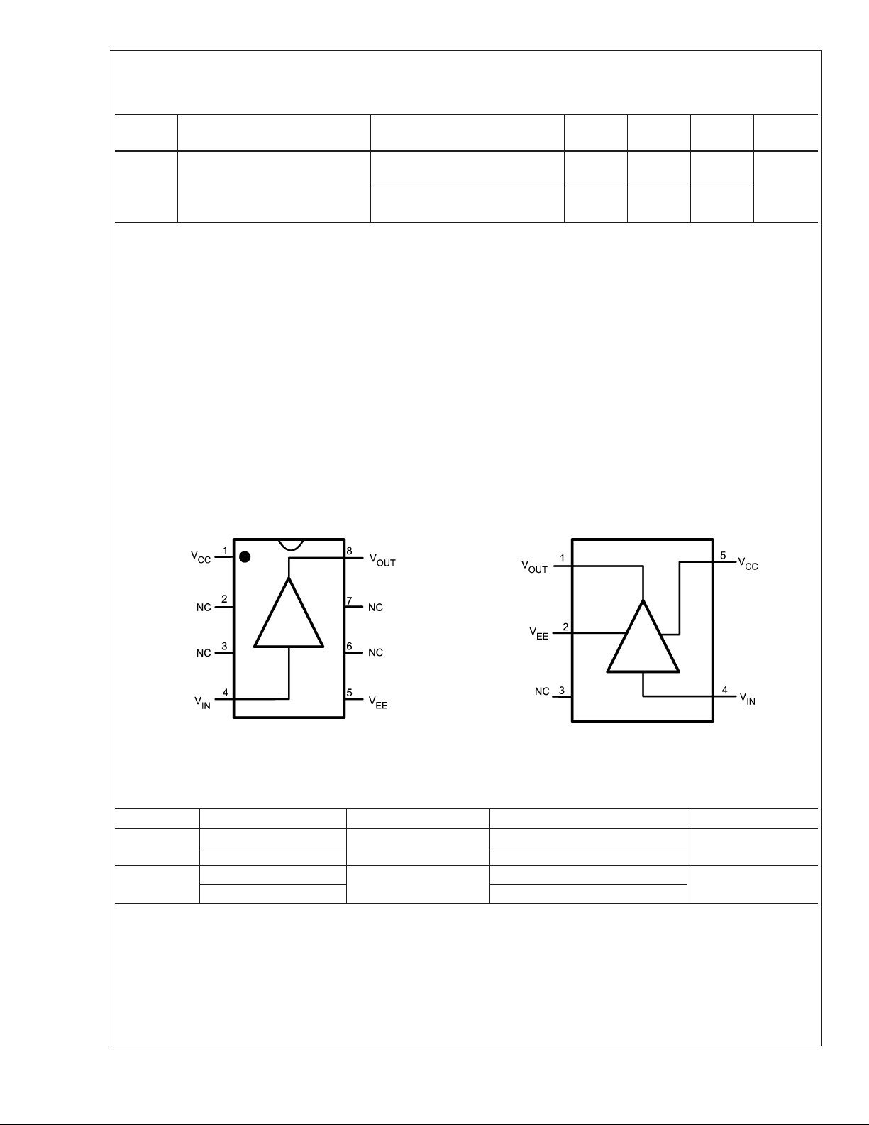
Connection Diagrams
8-Pin SOIC 5-Pin SOT23
Top View
20064134
Top View
20064135
Ordering Information
Package Part Number Package Marking Transport Media NSC Drawing
8-Pin SOIC LMH6559MA LMH6559MA 95 Units/Rail M08A
LMH6559MAX 2.5k Units Tape and Reel
5-Pin SOT23 LMH6559MF B05A 1k Units Tape and Reel MF05A
LMH6559MFX 3k Units Tape and Reel
www.national.com 6
LMH6559
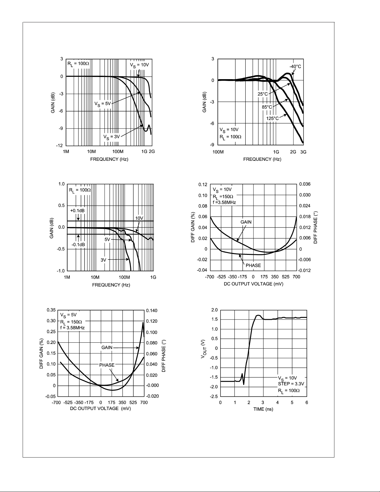
Typical Performance Characteristics At T
fied.
Frequency Response Frequency Response Over Temperature
20064101 20064132
Gain Flatness Differential Gain and Phase
= 25˚C; V+= +5V; V−= −5V; Unless otherwise speci-
J
20064102
Differential Gain and Phase Transient Response Positive
20064104
20064103
20064107
www.national.com7

Typical Performance Characteristics At T
specified. (Continued)
LMH6559
Transient Response Negative for Various V
Transient Response Negative Transient Response Positive for Various V
20064108 20064106
SUPPLY
= 25˚C; V+= +5V; V−= −5V; Unless otherwise
J
Harmonic Distortion vs. V
OUT
@
SUPPLY
5MHz
20064105
Harmonic Distortion vs. V
@
10MHz Harmonic Distortion vs. V
OUT
20064110
www.national.com 8
OUT
@
20064109
20MHz
20064114

LMH6559
Typical Performance Characteristics At T
specified. (Continued)
THD vs. V
for Various Frequencies Voltage Noise
OUT
20064111
Linearity V
OUT
vs. V
IN
= 25˚C; V+= +5V; V−= −5V; Unless otherwise
J
VOSvs. V
SUPPLY
for 3 Units
20064113
VOSvs. V
20064112
for Unit 1 VOSvs. V
SUPPLY
20064123 20064124
SUPPLY
20064122
for Unit 2
www.national.com9

Typical Performance Characteristics At T
specified. (Continued)
LMH6559
V
OS
vs. V
for Unit 3 IBvs. V
SUPPLY
= 25˚C; V+= +5V; V−= −5V; Unless otherwise
J
(Note 10)
SUPPLY
20064125
R
vs. Frequency PSRR vs. Frequency
OUT
20064115 20064116
I
SUPPLY
vs. V
SUPPLY
I
SUPPLY
vs. V
20064126
IN
20064127
www.national.com 10
20064121

LMH6559
Typical Performance Characteristics At T
specified. (Continued)
V
vs. I
OUT
IOSinking vs. V
Sinking V
OUT
20064128
SUPPLY
= 25˚C; V+= +5V; V−= −5V; Unless otherwise
J
vs. I
OUT
IOSourcing vs. V
OUT
Sourcing
SUPPLY
20064129
20064131
20064130
Small Signal Pulse Response Large Signal Pulse Response@VS=3V
20064117
20064118
www.national.com11

Typical Performance Characteristics At T
specified. (Continued)
LMH6559
Large Signal Pulse Response
@
VS= 5V Large Signal Pulse Response@VS= 10V
= 25˚C; V+= +5V; V−= −5V; Unless otherwise
J
20064119
20064120
www.national.com 12

Application Notes
USING BUFFERS
A buffer is an electronic device delivering current gain but no
voltage gain. It is used in cases where low impedances need
to be driven and more drive current is required. Buffers need
a flat frequency response and small propagation delay. Furthermore, the buffer needs to be stable under resistive,
capacitive and inductive loads. High frequency buffer applications require that the buffer be able to drive transmission
lines and cables directly.
LMH6559
20064138
FIGURE 3.
IN WHAT SITUATION WILL WE USE A BUFFER?
In case of a signal source not having a low output impedance
one can increase the output drive capability by using a
buffer. For example, an oscillator might stop working or have
frequency shift which is unacceptably high when loaded
heavily. A buffer should be used in that situation. Also in the
case of feeding a signal to an A/D converter it is recommended that the signal source be isolated from the A/D
converter. Using a buffer assures a low output impedance,
the delivery of a stable signal to the converter, and accommodation of the complex and varying capacitive loads that
the A/D converter presents to the OpAmp. Optimum value is
often found by experimentation for the particular application.
The use of buffers is strongly recommended for the handling
of high frequency signals, for the distribution of signals
through transmission lines or on pcb’s, or for the driving of
external equipment. There are several driving options:
Use one buffer to drive one transmission line (see Figure
•
1)
Use one buffer to drive to multiple points on one trans-
•
mission line (see Figure 2)
Use one buffer to drive several transmission lines each
•
driving a different receiver. (see Figure 3)
20064136
FIGURE 1.
In these three options it is seen that there is more than one
preferred method to reach an (end) point on a transmission
line. Until a certain point the designer can make his own
choice but the designer should keep in mind never to break
the rules about high frequency transport of signals. An explanation follows in the text below.
TRANSMISSION LINES
Introduction to transmission lines. The following is an overview of transmission line theory. Transmission lines can be
used to send signals from DC to very high frequencies. At all
points across the transmission line, Ohm’s law must apply.
For very high frequencies, parasitic behavior of the PCB or
cables comes into play. The type of cable used must match
the application. For example an audio cable looks like a coax
cable but is unusable for radar frequencies at 10GHz. In this
case one have to use special coax cables with lower attenuation and radiation characteristics.
Normally a pcb trace is used to connect components on a
pcb board together. An important considerations is the
amount of current carried by these pcb traces. Wider pcb
traces are required for higher current densities and for applications where very low series resistance is needed. When
routed over a ground plane, pcb traces have a defined
Characteristic Impedance. In many design situations characteristic impedance is not utilized. In the case of high
frequency transmission, however it is necessary to match
the load impedance to the line characteristic impedance
(more on this later). Each trace is associated with a certain
amount of series resistance and series inductance plus each
trace exhibits parallel capacitance to the ground plane. The
combination of these parameters defines the line’s characteristic impedance. The formula with which we calculate this
impedance is as follows:
=√(L/C)
Z
0
In this formula L and C are the value/unit length, and R is
assumed to be zero. C and L are unknown in many cases so
we have to follow other steps to calculate the Z
. The char-
0
acteristic impedance is a function of the geometry of the
cross section of the line. In (Figure 4) we see three cross
sections of commonly used transmission lines.
FIGURE 2.
20064137
www.national.com13

Application Notes (Continued)
LMH6559
FIGURE 4.
can be calculated by knowing some of the physical di-
Z
0
mensions of the pcb line, such as pcb thickness, width of the
trace and e
transmission line theory for calculating Z
e
relative dielectric constant
r
h pcb height
W trace width
th thickness of the copper
If we ignore the thickness of the copper in comparison to the
width of the trace then we have the following equation:
With this formula it is possible to calculate the line impedance vs. the trace width. Figure 5 shows the impedance
associated with a given line width. Using the same formula it
is also possible to calculate what happens when e
over a certain range of values. Varying the e
1 to 10 gives a variation for the Characteristic Impedance of
about 40Ω from 80Ω to 38Ω. Most transmission lines are
designed to have 50Ω or 75Ω impedance. The reason for
that is that in many cases the pcb trace has to connect to a
cable whose impedance is either 50Ω or 75Ω. As shown e
and the line width influence this value.
, relative dielectric constant. The formula given in
r
is as follows:
0
over a range of
r
20064139
r
(1)
(2)
varies
20064142
FIGURE 5.
Next, there will be a discussion of some issues associated
with the interaction of the transmission line at the source and
at the load.
Connecting a load using a transmission line
In most cases, it is unrealistic to think that we can place a
driver or buffer so close to the load that we don’t need a
transmission line to transport the signal. The pcb trace
length between a driver and the load may affect operation
depending upon the operating frequency. Sometimes it is
possible to do measurements by connecting the DUT directly
to the analyzer. As frequencies become higher the short
lines from the DUT to the analyzer become long lines. When
this happens there is a need to use transmission lines. The
next point to examine is what happens when the load is
connected to the transmission line. When driving a load, it is
important to match the line and load impedance, otherwise
reflections will occur and this phenomena will distort the
signal. If a transient is applied at T = 0 (Figure 6, trace A) the
resultant waveform may be observed at the start point of the
transmission line. At this point (begin) on the transmission
line the voltage increases to (V) and the wave front travels
along the transmission line and arrives at the load at T = 10.
r
At any point across along the lineI=V/Z
impedance of the transmission line. For an applied transient
of 2V with Z
=50Ω the current from the buffer output stage
0
, where Z0is the
0
is 40mA. Many vintage opamps cannot deliver this level of
current because of an output current limitation of about
20mA or even less. At T = 10 the wave front arrives at the
load. Since the load is perfectly matched to the transmission
line all of the current traveling across the line will be absorbed and there will be no reflections. In this case source
and load voltages are exactly the same. When the load and
the transmission line have unequal values of impedance a
different situation results. Remember there is another basic
which says that energy cannot be lost. The power in the
transmission line is P = V
2
/50 = 80mW. Assume a load of 75Ω. In that case a
is 2
2
/R. In our example the total power
power of 80mW arrives at the 75Ω load and causes a
voltage of the proper amplitude to maintain the incoming
power.
www.national.com 14

Application Notes (Continued)
(3)
The voltage wavefront of 2.45V will now set about traveling
back over the transmission line towards the source, thereby
resulting in a reflection caused by the mismatch. On the
other hand if the load is less then 50Ω the backwards
traveling wavefront is subtracted from the incoming voltage
of 2V. Assume the load is 40Ω. Then the voltage across the
load is:
(4)
This voltage is now traveling backwards through the line
toward the start point. In the case of a sinewave interferences develop between the incoming waveform and the
backwards-going reflections, thus distorting the signal. If
there is no load at all at the end point the complete transient
of 2V is reflected and travels backwards to the beginning of
the line. In this case the current at the endpoint is zero and
the maximum voltage is reflected. In the case of a short at
the end of the line the current is at maximum and the voltage
is zero.
cations, amplifier gain is set to 2 in order to realize an overall
gain of 1. Many operational amplifiers have a relatively flat
frequency response when set to a gain of two compared to
unity gain. In trace B it is seen that, if the voltage reaches the
end of the transmission line, the line is perfectly matched
and no reflections will occur. The end point voltage stays at
half the output voltage of the opamp or buffer.
Driving more than one input
Another transmission line possibility is to route the trace via
several points along a transmission line (Figure 2) This is
only possible if care is taken to observe certain restrictions.
Failure to do so will result in impedance discontinuities that
will cause distortion of the signal. In the configuration of
Figure 2 there is a transmission line connected to the buffer
output and the end of the line is terminated with Z
. We have
0
seen in the section ’Connecting a load using a transmission
line’ that for the condition above, the signal throughout the
entire transmission line has the same value, that the value is
the nominal value initiated by the opamp output, and no
reflections occur at the end point. Because of the lack of
reflections no interferences will occur. Consequently the signal has every where on the line the same amplitude. This
allows the possibility of feeding this signal to the input port of
any device which has high ohmic impedance and low input
capacitance. In doing so keep in mind that the transient
arrives at different times at the connected points in the
transmission line. The speed of light in vacuum, which is
about3*10
a cable down to a value of about2*10
8
m/sec, reduces through a transmission line or
8
m/sec. The distance
the signal will travel in 1ns is calculated by solving the
following formula:
*
t
S=V
Where
S = distance
V = speed in the cable
t = time
8
This calculation gives the following result: s = 2*10
* 1*10
= 0.2m
That is for each nanosecond the wave front shifts 20cm over
the length of the transmission line. Keep in mind that in a
distance of just 2cm the time displacement is already 100ps.
LMH6559
−9
20064145
FIGURE 6.
Using serial and parallel termination
Many applications, such as video, use a series resistance
between the driver and the transmission line (see Figure 1).
In this case the transmission line is terminated with the
characteristic impedance at both ends of the line. See Figure
6 trace B. The voltage traveling through the transmission line
is half the voltage seen at the output of the buffer, because
the series resistor in combination with Z
forms a two-to-one
0
voltage divider. The result is a loss of 6dB. For video appli-
Using serial termination to more than one
transmission line
Another way to reach several points via a transmission line is
to start several lines from one buffer output (see Figure 3).
This is possible only if the output can deliver the needed
current into the sum of all transmission lines. As can be seen
in this figure there is a series termination used at the beginning of the transmission line and the end of the line has no
termination. This means that only the signal at the endpoint
is usable because at all other points the reflected signal will
cause distortion over the line. Only at the endpoint will the
measured signal be the same as at the startpoint. Referring
to Figure 6 trace C, the signal at the beginning of the line has
a value of V/2 and at T = 0 this voltage starts traveling
towards the end of the transmission line. Once at the endpoint the line has no termination and 100% reflection will
occur. At T = 10 the reflection causes the signal to jump to 2V
and to start traveling back along the line to the buffer (see
Figure 6 trace D). Once the wavefront reaches the series
termination resistor, provided the termination value is Z
0
, the
wavefront undergoes total absorption by the termination.
This is only true if the output impedance of the buffer/driver
is low in comparison to the characteristic impedance Z
.At
0
www.national.com15

Application Notes (Continued)
this moment the voltage in the whole transmission line has
LMH6559
the nominal value of 2V (see Figure 6 trace E). If the three
transmission lines each have a different length the particular
point in time at which the voltage at the series termination
resistor jumps to 2V is different for each case. However, this
transient is not transferred to the other lines because the
output of the buffer is low and this transient is highly attenuated by the combination of the termination resistor and the
output impedance of the buffer. A simple calculation illustrates the point. Assume that the output impedance is 5Ω.
For the frequency of interest the attenuation is V
= 11, where A and B are the points in Figure 3. In this case
the voltage caused by the reflection is 2/11 = 0.18V. This
voltage is transferred to the remaining transmission lines in
sequence and following the same rules as before this voltage is seen at the end points of those lines. The lower the
output resistance the higher the decoupling between the
different lines. Furthermore one can see that at the endpoint
of these transmission lines there is a normal transient equal
to the original transient at the beginning point. However at all
other points of the transmission line there is a step voltage at
different distances from the startpoint depending at what
point this is measured (see trace D).
B/VA
= 55/5
As calculated before in the section ’Driving more than one
input’ the signal travels 20cm/ns so in 5ns this distance
indicated distance is 1m. So this example is easily verified.
APPLYING A CAPACITIVE LOAD
The assumption of pure resistance for the purpose of connecting the output stage of a buffer or opamp to a load is
appropriate as a first approximation. Unfortunately that is
only a part of the truth. Associated with this resistor is a
capacitor in parallel and an inductor in series. Any capacitance such as C
-1 which is connected directly to the output
L
stage is active in the loop gain as seen in Figure 8. Output
capacitance, present also at the minus input in the case of a
buffer, causes an increasing phase shift leading to instability
or even oscillation in the circuit.
Measuring the length of a transmission line
An open transmission line can be used to measure the
length of a particular transmission line. As can be seen in
Figure 7 the line of interest has a certain length. A transient
is applied at T = 0 and at that point in time the wavefront
starts traveling with an amplitude of V/2 towards the end of
the line where it is reflected back to the startpoint.
20064146
FIGURE 7.
To calculate the length of the line it is necessary to measure
immediately after the series termination resistor. The voltage
at that point remains at half nominal voltage, thus V/2, until
the reflection returns and the voltage jumps to V. During an
interval of 5ns the signal travels to the end of the line where
the wave front is reflected and returns to the measurement
point. During the time interval when the wavefront is traveling to the end of the transmission line and back the voltage
has a value of V/2. This interval is 10ns. The length can be
calculated with the following formula: S = (V*T)/2
20064148
FIGURE 8.
Unfortunately the leads of the output capacitor also contain
series inductors which become more and more important at
high frequencies. At a certain frequency this series capacitor
and inductor forms an LC combination which becomes series resonant. At the resonant frequency the reactive component vanishes leaving only the ohmic resistance (R-1 or
R-2) of the series L/C combination. (see Figure 9).
20064149
FIGURE 9.
Consider a frequency sweep over the entire spectrum for
which the LMH6559 high frequency buffer is active. In the
first instance peaking occurs due to the parasitic capacitance connected at the load whereas at higher frequencies
the effects of the series combination of L and C become
noticeable. This causes a distinctive dip in the output frequency sweep and this dip varies depending upon the particular capacitor as seen in Figure 10.
(5)
www.national.com 16

Application Notes (Continued)
20064150
FIGURE 10.
To minimize peaking due to CL a series resistor for the
purpose of isolation from the output stage should be used. A
low valued resistor will minimize the influence of such a load
capacitor. In a 50Ω system as is common in high frequency
circuits a 50Ω series resistor is often used. Usage of the
series resistor, as seen in Figure 11 eliminates the peaking
but not the dip. The dip will vary with the particular capacitor.
Using a resistor in series with a capacitor creates in a single
pole situation a 6dB/oct rolloff. However, at high frequencies
the internal inductance is appreciable and forms a series LC
combination with the capacitor. Choice of a higher valued
resistor, for example 500 to 1kΩ, and a capacitor of hundreds of pF’s provides the expected response at lower frequencies.
USING GROUND PLANES
The use of ground planes is recommended both for providing a low impedance path to ground (or to one of the other
supply voltages) and also for forming effective controlled
impedance transmission lines for the high frequency signal
flow on the board. Multilayer boards often make use of inner
conductive layers for routing supply voltages. These supply
voltage layers form a complete plane rather than using discrete traces to connect the different points together for the
specified supply. Signal traces on the other hand are routed
on outside layers both top and bottom. This allows for easy
access for measurement purposes. Fortunately, only very
high density boards have signal layers in the middle of the
board. In an earlier section, the formula for Z
was derived
0
as:
(6)
The width of a trace is determined by the thickness of the
board. In the case of a multilayer board the thickness is the
space between the trace and the first supply plane under this
trace layer. By common practice, layers do not have to be
evenly divided in the construction of a pcb. Refer to Figure
12. The design of a transmission line design over a pcb is
based upon the thickness of the different internal layers and
of the board material. The pcb manufacturer can
the e
r
supply information about important specifications. For example, a nominal 1.6mm thick pcb produces a 50Ω trace for
a calculated width of 2.9mm. If this layer has a thickness of
0.35mm and for the same e
, the trace width for 50Ω should
r
be of 0.63mm, as calculated from Equation 7, a derivation
from Equation 6.
LMH6559
FIGURE 11.
20064151
(7)
20064154
FIGURE 12.
Using a trace over a ground plane has big advantages over
the use of a standard single or double sided board. The main
advantage is that the electric field generated by the signal
transported over this trace is fixed between the trace and the
ground plane e.g. there is almost no possibility of radiation
(seeFigure 13).
www.national.com17

Application Notes (Continued)
LMH6559
FIGURE 13.
This effect works to both sides because the circuit will not
generate radiation but the circuit is also not sensible if exposed to a certain radiation level. The same is also noticeable when placing components flat on the printed circuit
board. Standard through hole components when placed upright can act as an antenna causing an electric field which
could be picked up by a nearby upright component. If placed
directly at the surface of the pcb this influence is much lower.
The effect of variation for e
When using pcb material the erhas a certain shift over the
used frequency spectrum, so if necessary to work with very
accurate trace impedances one must taken into account for
which frequency region the design has to be functional.
Figure 14 (http://www.isola.de) gives an example what the
drift in e
will be when using the pcb material produced by
r
Isola. If working at frequencies of 100MHz then a 50Ω trace
has a width of 3.04mm for standard 1.6mm FR4 pcb material, and the same trace needs a width of 3.14mm. for
frequencies around 10GHz.
r
20064155
Careful attention to power line distribution leads to improved
overall circuit performance. This is especially valid for analog
circuits which are more sensitive to spurious noise and other
unwanted signals.
20064157
FIGURE 15.
As demonstrated in Figure 15 the power lines are routed
from both sides on the pcb. In this case a current loop is
created as indicated by the dotted line. This loop can act as
an antenna for high frequency signals which makes the
circuit sensitive to R
radiation. A better way to route the
F
power traces can be seen in the following setup. (see Figure
16)
20064156
FIGURE 14.
Routing power traces
Power line traces routed over a pcb should be kept together
for best practice. If not a ground loop will occur which may
cause more sensitivity to radiation. Also additional ground
trace length may lead to more ringing on digital signals.
www.national.com 18
20064158
FIGURE 16.
In this arrangement the power lines have been routed in
order to avoid ground loops and to minimize sensitivity to
noise etc. The same technique is valid when routing a high
frequent signal over a board which has no ground plane. In
that case is it good practice to route the high frequency
signal alongside a ground trace. A still better way to create a
pcb carrying high frequency signals is to use a pcb with a
ground plane or planes.

LMH6559
Application Notes (Continued)
Discontinuities in a ground plane
A ground plane with traces routed over this plane results in
the build up of an electric field between the trace and the
ground plane as seen in Figure 13. This field is build up over
the entire routing of the trace. For the highest performance
the ground plane should not be interrupted because to do so
will cause the field lines to follow a roundabout path. In
Figure 17 it was necessary to interrupt the ground plane with
a crossing trace. This interruption causes the return current
to follow a longer route than the signal path follows to
overcome the discontinuity.
If the overall density becomes too high it is better to make a
design which contains additional metal layers such that the
ground planes actually function as ground planes. The costs
for such a pcb are increased but the payoff is in overall
effectiveness and ease of design.
Ground planes at top and bottom layer of a pcb
In addition to the bottom layer ground plane another useful
practice is to leave as much copper as possible at the top
layer. This is done to reduce the amount of copper to be
removed from the top layer in the chemical process. This
causes less pollution of the chemical baths allowing the
manufacturer to make more pcb’s with a certain amount of
chemicals. Connecting this upper copper to ground provides
additional shielding and signal performance is enhanced.
For lower frequencies this is specifically true. However, at
higher frequencies other effects become more and more
important such that unwanted coupling may result in a reduction in the bandwidth of a circuit. In the design of a test
circuit for the LMH6559 this effect was clearly noticeable and
the useful bandwidth was reduced from 1500MHz to around
850MHz.
20064159
FIGURE 17.
If needed it is possible to bypass the interruption with traces
that are parallel to the signal trace in order to reduce the
negative effects of the discontinuity in the ground plane. In
doing so, the current in the ground plane closely follows the
signal trace on the return path as can be seen in Figure 18.
Care must be taken not to place too many traces in the
ground plane or the ground plane effectively vanishes such
that even bypasses are unsuccessful in reducing negative
effects.
20064160
FIGURE 18.
20064161
FIGURE 19.
As can be seen in Figure 19 the presence of a copper field
close to the transmission line to and from the buffer causes
unwanted coupling effects which can be seen in the dip at
about 850MHz. This dip has a depth of about 5dB for the
case when all of the unused space is filled with copper. In
case of only one area being filled with copper this dip is
about 9dB.
Pcb board layout and component selection
Sound practice in the area of high frequency design requires
that both active and passive components be used for the
purposes for which they were designed. It is possible to
amplify signals at frequencies of several hundreds of MHz
using standard through hole resistors. Surface mount devices, however, are better suited for this purpose. Surface
mount resistors and capacitors are smaller and therefore
parasitics are of lower value and therefore have less influence on the properties of the amplifier. Another important
issue is the pcb itself, which is no longer a simple carrier for
all the parts and a medium to interconnect them. The pcb
board becomes a real component itself and consequently
contributes its own high frequency properties to the overall
performance of the circuit. Sound practice dictates that a
www.national.com19

Application Notes (Continued)
design have at least one ground plane on a pcb which
LMH6559
provides a low impedance path for all decoupling capacitors
and other ground connections. Care should be taken especially that on- board transmission lines have the same impedance as the cables to which they are connected - 50Ω for
most applications and 75Ω in case of video and cable TV
applications. Such transmission lines usually require much
wider traces on a standard double sided PCB board than
needed for a ’normal’ trace. Another important issue is that
inputs and outputs must not ’see’ each other. This occurs if
inputs and outputs are routed together over the pcb with only
a small amount of physical separation, particularly when
there is a high differential in signal level between them.
Furthermore components should be placed as flat and low
as possible on the surface of the PCB. For higher frequencies a long lead can act as a coil, a capacitor or an antenna.
A pair of leads can even form a transformer. Careful design
of the pcb avoids oscillations or other unwanted behaviors.
For ultra high frequency designs only surface mount components will give acceptable results. (for more information see
OA-15).
NSC suggests the following evaluation boards as a guide for
high frequency layout and as an aid in device testing and
characterization.
Device Package Evaluation Board
Part Number
LMH6559MA SOIC-8 CLC730245
LMH6559MAX SOIC-8 CLC730245
LMH6559MF SOT23-5 CLC730136
LMH6559MFX SOT23-5 CLC730136
These free evaluation boards are shipped when a device
sample request is placed with National Semiconductor.
POWER SEQUENCING OF THE LMH6559
Caution should be exercised in applying power to the
LMH6559. When the negative power supply pin is left floating it is recommended that other pins, such as positive
supply and signal input should also be left unconnected. If
the ground is floating while other pins are connected the
input circuitry is effectively biased to ground, with a mostly
low ohmic resistor, while the positive power supply is capable of delivering significant current through the circuit. This
causes a high input bias current to flow which degrades the
input junction. The result is an input bias current which is out
of specification. When using inductive relays in an application care should be taken to connect first both power connections before connecting the bias resistor to the input.
www.national.com 20

Physical Dimensions inches (millimeters)
unless otherwise noted
NS Package Number M08A
LMH6559
8-Pin SOIC
5-Pin SOT23
NS Package Number MF05A
www.national.com21

LMH6559 High-Speed, Closed-Loop Buffer
Notes
LIFE SUPPORT POLICY
NATIONAL’S PRODUCTS ARE NOT AUTHORIZED FOR USE AS CRITICAL COMPONENTS IN LIFE SUPPORT
DEVICES OR SYSTEMS WITHOUT THE EXPRESS WRITTEN APPROVAL OF THE PRESIDENT AND GENERAL
COUNSEL OF NATIONAL SEMICONDUCTOR CORPORATION. As used herein:
1. Life support devices or systems are devices or
systems which, (a) are intended for surgical implant
into the body, or (b) support or sustain life, and
whose failure to perform when properly used in
accordance with instructions for use provided in the
2. A critical component is any component of a life
support device or system whose failure to perform
can be reasonably expected to cause the failure of
the life support device or system, or to affect its
safety or effectiveness.
labeling, can be reasonably expected to result in a
significant injury to the user.
National Semiconductor
Americas Customer
Support Center
Email: new.feedback@nsc.com
Tel: 1-800-272-9959
www.national.com
National does not assume any responsibility for use of any circuitry described, no circuit patent licenses are implied and National reserves the right at any time without notice to change said circuitry and specifications.
National Semiconductor
Europe Customer Support Center
Fax: +49 (0) 180-530 85 86
Email: europe.support@nsc.com
Deutsch Tel: +49 (0) 69 9508 6208
English Tel: +44 (0) 870 24 0 2171
Français Tel: +33 (0) 1 41 91 8790
National Semiconductor
Asia Pacific Customer
Support Center
Fax: +65-6250 4466
Email: ap.support@nsc.com
Tel: +65-6254 4466
National Semiconductor
Japan Customer Support Center
Fax: 81-3-5639-7507
Email: jpn.feedback@nsc.com
Tel: 81-3-5639-7560
 Loading...