


查询LMH6551供应商
LMH6551
Differential, High Speed Op Amp
LMH6551 Differential, High Speed Op Amp
February 2005
General Description
The LMH™6551 is a high performance voltage feedback
differential amplifier. The LMH6551 has the high speed and
low distortion necessary for driving high performance ADCs
as well as the current handling capability to drive signals
over balanced transmission lines like CAT 5 data cables. The
LMH6551 can handle a wide range of video and data formats.
With external gain set resistors, the LMH6551 can be used
at any desired gain. Gain flexibility coupled with high speed
makes the LMH6551 suitable for use as an IF amplifier in
high performance communications equipment.
The LMH6551 is available in the space saving SOIC and
MSOP packages.
Typical Application
Features
n 370 MHz −3 dB bandwidth (V
n 50 MHz 0.1 dB bandwidth
n 2400 V/µs slew Rate
n 18 ns settling time to 0.05%
n −94/−96 dB HD2/HD3
@
OUT
5 MHz
Applications
n Differential AD driver
n Video over twisted pair
n Differential line driver
n Single end to differential converter
n High speed differential signaling
n IF/RF amplifier
n SAW filter buffer/driver
= 0.5 VPP)
Single Ended Input Differential Output.
Gain = A
LMH™is a trademark of National Semiconductor Corporation.
© 2005 National Semiconductor Corporation DS201332 www.national.com
Where VINis measured single ended and V
V=RF/RG
is measured differentially. (Each individual output will equal±VIN/2.)
OUT
20133210
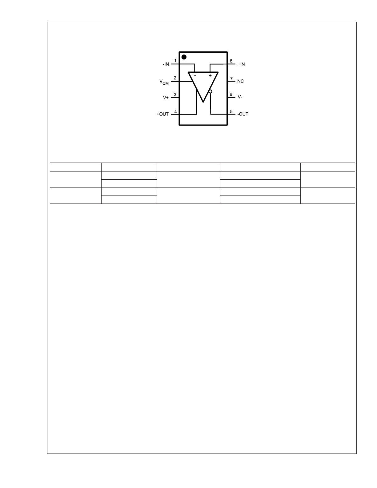
Connection Diagram
LMH6551
Ordering Information
Package Part Number Package Marking Transport Media NSC Drawing
8-Pin SOIC
8–Pin MSOP
8-Pin SOIC & MSOP
Top View
LMH6551MA
LMH6551MAX 2.5k Units Tape and Reel
LMH6551MM
LMH6551MMX 3.5k Units Tape and Reel
LMH6551MA
AU1A
20133208
95/Rails
1k Units Tape and Reel
M08A
MUA08A
www.national.com 2

LMH6551
Absolute Maximum Ratings (Note 1)
If Military/Aerospace specified devices are required,
please contact the National Semiconductor Sales Office/
Distributors for availability and specifications.
ESD Tolerance (Note 5)
Soldering Information
Infrared or Convection (20 sec) 235˚C
Wave Soldering (10 sec) 260˚C
Operating Ratings (Note 1)
Human Body Model 2000V
Machine Model 200V
Supply Voltage 13.2V
Common Mode Input Voltage
Maximum Input Current (pins 1, 2,
7, 8) 30mA
Maximum Output Current (pins 4, 5) (Note 3)
±
5V Electrical Characteristics (Note 2)
±
Vs
Operating Temperature Range −40˚C to +125˚C
Storage Temperature Range −65˚C to +150˚C
Total Supply Voltage 3V to 12V
Package Thermal Resistance (θ
) (Note 4)
JA
8-Pin MSOP 235˚C/W
8-Pin SOIC 150˚C/W
Single ended in differential out, TA= 25˚C, G = +1, VS=±5V, VCM= 0V, RF=RG= 365Ω,RL= 500Ω;; Unless specified Bold-
face limits apply at the temperature extremes.
Symbol Parameter Conditions Min
(Note 8)
Typ
(Note 7)
Max
(Note 8)
Units
AC Performance (Differential)
SSBW Small Signal −3 dB Bandwidth V
LSBW Large Signal −3 dB Bandwidth V
Large Signal −3 dB Bandwidth V
0.1 dB Bandwidth V
OUT
OUT
OUT
OUT
= 0.5 V
=2V
=4V
=2V
PP
PP
PP
PP
370 MHz
340 MHz
320 MHz
50 MHz
Slew Rate 4V Step(Note 6) 2400 V/µs
Rise/Fall Time 2V Step 1.8 ns
Settling Time 2V Step, 0.05% 18 ns
V
Pin AC Performance (Common Mode Feedback Amplifier)
CM
Common Mode Small Signal
V
bypass capacitor removed 200 MHz
CM
Bandwidth
Distortion and Noise Response
HD2 V
HD2 V
HD3 V
HD3 V
e
n
i
n
Input Referred Voltage Noise Freq ≥ 1 MHz 6.0 nV/
Input Referred Noise Current Freq ≥ 1 MHz 1.5 pA/
=2VPP,f=5MHz, RL=800Ω −94 dBc
O
=2VPP, f = 20MHz, RL=800Ω −85 dBc
O
=2VPP,f=5MHz, RL=800Ω −96 dBc
O
=2VPP,f=20MHz, RL=800Ω −72 dBc
O
Input Characteristics (Differential)
V
OSD
Input Offset Voltage Differential Mode, VID=0,VCM= 0 0.5
Input Offset Voltage Average
(Note 10) −0.8 µV/˚C
±
4
±
6
Temperature Drift
I
BI
Input Bias Current (Note 9) -4 0
-10
Input Bias Current Average
(Note 10) −2.6 nA/˚C
Temperature Drift
Input Bias Difference Difference in Bias currents
0.03 µA
between the two inputs
CMRR Common Mode Rejection Ratio DC, V
R
IN
C
IN
CMVR Input Common Mode Voltage
Input Resistance Differential 5 MΩ
Input Capacitance Differential 1 pF
CMRR
Range
= 0V, VID= 0V 72 80 dBc
CM
>
53dB +3.1
−4.6
+3.2
−4.7
VCMPin Input Characteristics (Common Mode Feedback Amplifier)
mV
µA
V
www.national.com3

±
5V Electrical Characteristics (Note 2) (Continued)
Single ended in differential out, TA= 25˚C, G = +1, VS=±5V, VCM= 0V, RF=RG= 365Ω,RL= 500Ω;; Unless specified Boldface limits apply at the temperature extremes.
LMH6551
Symbol Parameter Conditions Min
(Note 8)
V
OSC
Input Offset Voltage Common Mode, VID= 0 0.5
Input Offset Voltage Average
(Note 10) 8.2 µV/˚C
Typ
(Note 7)
Max
(Note 8)
±
5
±
8
Temperature Drift
Input Bias Current (Note 9) −2 µA
V
CMRR VID= 0V, 1V step on VCMpin,
CM
measure V
OD
70 75 dB
Input Resistance 25 kΩ
Common Mode Gain ∆V
O,CM
/∆V
CM
0.995 0.999 1.005 V/V
Output Performance
Output Voltage Swing Single Ended, Peak to Peak
Output Common Mode Voltage
V
ID
=0V,
±
±
±
7.38
7.18
3.69
±
7.8 V
±
3.8 V
Range
I
I
OUT
SC
Linear Output Current V
OUT
=0V
Short Circuit Current Output Shorted to Ground
= 3V Single Ended(Note 3)l
V
IN
Output Balance Error ∆V
Common Mode
OUT
/∆V
OUT
DIfferential , V
OUT
= 0.5
±
50
±
65 mA
140 mA
−70 dB
Vpp Differential,f=10MHz
Miscellaneous Performance
A
VOL
PSRR Power Supply Rejection Ratio DC, ∆V
Open Loop Gain Differential 70 dB
=±1V 74 90 dB
S
Supply Current R
∞
=
L
11 12.5 14.5
16.5
Units
mV
mA
5V Electrical Characteristics (Note 2)
Single ended in differential out, TA= 25˚C, G = +1, VS= 5V, VCM= 2.5V, RF=RG= 365Ω,RL= 500Ω; ; Unless specifiedBoldface limits apply at the temperature extremes.
Symbol Parameter Conditions Min
(Note 8)
SSBW Small Signal −3 dB Bandwidth R
LSBW Large Signal −3 dB Bandwidth R
0.1 dB Bandwidth V
= 500Ω,V
L
= 500Ω,V
L
=2V
OUT
= 0.5 V
OUT
OUT
PP
=2V
PP
PP
Slew Rate 4V Step(Note 6) 1800 V/µs
Rise/Fall Time, 10% to 90% 4V Step 2 ns
Settling Time 4V Step, 0.05% 17 ns
V
Pin AC Performance (Common Mode Feedback Amplifier)
CM
Common Mode Small Signal
Bandwidth
Distortion and Noise Response
HD2 2
HD2 V
HD3 3
HD3 V
e
n
i
n
nd
Harmonic Distortion VO=2VPP,f=5MHz, RL=800Ω −84 dBc
=2VPP,f=20MHz, RL=800Ω −69 dBc
rd
Harmonic Distortion VO=2VPP,f=5MHz, RL=800Ω −93 dBc
O
=2VPP,f=20MHz, RL=800Ω −67 dBc
O
Input Referred Noise Voltage Freq ≥ 1 MHz 6.0 nV/
Input Referred Noise Current Freq ≥ 1 MHz 1.5 pA/
Input Characteristics (Differential)
Typ
(Note 7)
Max
(Note 8)
350 MHz
300 MHz
50 MHz
170 MHz
Units
www.national.com 4
5V Electrical Characteristics (Note 2) (Continued)
Single ended in differential out, TA= 25˚C, G = +1, VS= 5V, VCM= 2.5V, RF=RG= 365Ω,RL= 500Ω; ; Unless specifiedBoldface limits apply at the temperature extremes.
Symbol Parameter Conditions Min
(Note 8)
V
OSD
Input Offset Voltage Differential Mode, VID=0,VCM= 0 0.5
Input Offset Voltage Average
(Note 10) −0.8 µV/˚C
Temperature Drift
I
BIAS
Input Bias Current (Note 9) −4 0
Input Bias Current Average
(Note 10) −3 nA/˚C
Temperature Drift
Input Bias Current Difference Difference in Bias currents between
the two inputs
CMRR Common-Mode Rejection Ratio DC, V
= 0V 70 78 dBc
ID
Input Resistance Differential 5 MΩ
Input Capacitance Differential 1 pF
V
ICM
Input Common Mode Range CMRR>53 dB +3.1
VCMPin Input Characteristics (Common Mode Feedback Amplifier)
Input Offset Voltage Common Mode, V
= 0 0.5
ID
Input Offset Voltage Average
Temperature Drift
Input Bias Current 3µA
V
CMRR VID=0,
CM
1V step on V
Input Resistance V
Common Mode Gain ∆V
pin to ground 25 kΩ
CM
/∆V
O,CM
pin, measure V
CM
CM
OD
0.995 0.991 1.005 V/V
Output Performance
V
OUT
I
OUT
I
SC
CMVR Output Common Mode Voltage
Output Voltage Swing Single Ended, Peak to Peak, VS=
±
2.5V, VCM=0V
Linear Output Current V
= 0V Differential
OUT
Output Short Circuit Current Output Shorted to Ground
= 3V Single Ended(Note 3)
V
IN
V
=0,VCMpin = 1.2V and 3.8V 3.72
ID
Range
Output Balance Error ∆V
/∆V
OUT
OUT
Common Mode
DIfferential , V
OUT
= 1Vpp
Differential,f=10MHz
Miscellaneous Performance
Open Loop Gain DC, Differential 70 dB
PSRR Power Supply Rejection Ratio DC, ∆V
I
S
Supply Current RL=
=±0.5V 72 88 dB
S
∞
+0.4
70 75 dB
±
2.4
±
45
1.23
10 11.5 13.5
Typ
(Note 7)
Max
(Note 8)
±
4
±
6
-10
0.03 µA
+3.2
+0.3
±
5
±
8
5.8 µV/˚C
±
2.8 V
±
60 mA
230 mA
3.8
1.2
−65 dB
15.5
Units
mV
mV
mA
LMH6551
µA
V
3.3V Electrical Characteristics (Note 2)
Single ended in differential out, TA= 25˚C, G = +1, VS= 3.3V, VCM= 1.65V, RF=RG= 365Ω,RL= 500Ω; ; Unless specified-
Boldface limits apply at the temperature extremes.
Symbol Parameter Conditions Min
(Note 8)
SSBW Small Signal −3 dB Bandwidth R
= 500Ω,V
L
OUT
= 0.5 V
PP
Typ
(Note 7)
Max
(Note 8)
320 MHz
www.national.com5
Units

3.3V Electrical Characteristics (Note 2) (Continued)
Single ended in differential out, TA= 25˚C, G = +1, VS= 3.3V, VCM= 1.65V, RF=RG= 365Ω,RL= 500Ω; ; Unless specified-
Boldface limits apply at the temperature extremes.
LMH6551
Symbol Parameter Conditions Min
(Note 8)
LSBW Large Signal −3 dB Bandwidth R
= 500Ω,V
L
OUT
=1V
PP
Slew Rate 1V Step(Note 6) 700 V/µs
Rise/Fall Time, 10% to 90% 1V Step 2 ns
V
Pin AC Performance (Common Mode Feedback Amplifier)
CM
Common Mode Small Signal
Bandwidth
Distortion and Noise Response
HD2 2
HD2 V
HD3 3
HD3 V
nd
Harmonic Distortion VO=1VPP,f=5MHz, RL=800Ω −93 dBc
=1VPP,f=20MHz, RL=800Ω −74 dBc
rd
Harmonic Distortion VO=1VPP,f=5MHz, RL=800Ω −85 dBc
O
=1VPP,f=20MHz, RL=800Ω −69 dBc
O
Input Characteristics (Differential)
V
OSD
Input Offset Voltage Differential Mode, VID=0,VCM=0 1 mV
Input Offset Voltage Average
(Note 10) 1.6 µV/˚C
Temperature Drift
I
BIAS
Input Bias Current (Note 9) −8 µA
Input Bias Current Average
(Note 10) 9.5 nA/˚C
Temperature Drift
Input Bias Current Difference Difference in Bias currents between
the two inputs
CMRR Common-Mode Rejection Ratio DC, V
= 0V 78 dBc
ID
Input Resistance Differential 5 MΩ
Input Capacitance Differential 1 pF
V
ICM
Pin Input Characteristics (Common Mode Feedback Amplifier)
V
CM
Input Common Mode Range CMRR>53 dB +1.5
Input Offset Voltage Common Mode, V
=0 1
ID
Input Offset Voltage Average
Temperature Drift
Input Bias Current 3µA
V
CMRR VID=0,
CM
1V step on V
pin, measure V
CM
OD
Input Resistance VCMpin to ground 25 kΩ
Common Mode Gain ∆V
O,CM
/∆V
CM
Output Performance
V
I
OUT
I
SC
OUT
Output Voltage Swing Single Ended, Peak to Peak, VS=
Linear Output Current V
Output Short Circuit Current Output Shorted to Ground
CMVR Output Common Mode Voltage
3.3V, V
OUT
V
IN
V
ID
= 1.65V
CM
= 0V Differential
= 2V Single Ended(Note 3)
=0,VCMpin = 1.2V and 2.1V 2.1
±
Range
Output Balance Error ∆V
Common Mode
OUT
/∆V
OUT
DIfferential , V
OUT
= 1Vpp
Differential,f=10MHz
Miscellaneous Performance
Open Loop Gain DC, Differential 70 dB
PSRR Power Supply Rejection Ratio DC, ∆V
=±0.5V 75 dB
S
0.75
±
30
Typ
(Note 7)
Max
(Note 8)
300 MHz
95 MHz
0.3 µA
+0.3
±
18.6 µV/˚C
60 dB
0.999 V/V
±
0.9 V
±
40 mA
200 mA
1.2
−65 dB
Units
5mV
V
www.national.com 6

3.3V Electrical Characteristics (Note 2) (Continued)
Single ended in differential out, TA= 25˚C, G = +1, VS= 3.3V, VCM= 1.65V, RF=RG= 365Ω,RL= 500Ω; ; Unless specified-
Boldface limits apply at the temperature extremes.
Symbol Parameter Conditions Min
(Note 8)
I
S
Note 1: Absolute Maximum Ratings indicate limits beyond which damage to the device may occur. Operating Ratings indicate conditions for which the device is
intended to be functional, but specific performance is not guaranteed. For guaranteed specifications, see the Electrical Characteristics tables.
Note 2: Electrical Table values apply only for factory testing conditions at the temperature indicated. Factory testing conditions result in very limited self-heating of
the device such that T
Note 3: The maximum output current (I
Note 4: The maximum power dissipation is a function of T
P
D
Note 5: Human body model: 1.5 kΩ in series with 100 pF. Machine model: 0Ω in series with 200pF.
Note 6: Slew Rate is the average of the rising and falling edges.
Note 7: Typical numbers are the most likely parametric norm.
Note 8: Limits are 100% production tested at 25˚C. Limits over the operating temperature range are guaranteed through correlation using Statistical Quality Control
(SQC) methods.
Note 9: Negative input current implies current flowing out of the device.
Note 10: Drift determined by dividing the change in parameter at temperature extremes by the total temperature change.
Note 11: Parameter is guaranteed by design.
Supply Current RL=
. No guarantee of parametric performance is indicated in the electrical tables under conditions of internal self-heating where T
J=TA
OUT
=(T
J(MAX)—TA
)/ θJA. All numbers apply for package soldered directly into a 2 layer PC board with zero air flow.
) is determined by device power dissipation limitations.
∞
, θJAand TA. The maximum allowable power dissipation at any ambient temperature is
J(MAX)
Typ
(Note 7)
Max
(Note 8)
Units
8mA
J
LMH6551
>
TA.
www.national.com7

Typical Performance Characteristics (T
Specified).
LMH6551
Frequency Response vs. Supply Voltage Frequency Response
20133214 20133215
Frequency Response vs. V
OUT
= 25˚C, VS=±5V, RL= 500Ω,RF= 365Ω,AV=1; Unless
A
Frequency Response vs. Capacitive Load
20133216
Suggested R
www.national.com 8
vs. Cap Load Suggested R
OUT
20133222 20133223
vs. Cap Load
OUT
20133221

LMH6551
Typical Performance Characteristics (T
Specified). (Continued)
1V
Pulse Response Single Ended Input 2 VPPPulse Response Single Ended Input
PP
20133226 20133227
Large Signal Pulse Response Output Common Mode Pulse Response
= 25˚C, VS=±5V, RL= 500Ω,RF= 365Ω,AV=1; Unless
A
20133235
Distortion vs. Frequency Distortion vs. Frequency
20133228
20133224
20133229
www.national.com9

Typical Performance Characteristics (T
Specified). (Continued)
LMH6551
Distortion vs. Frequency Distortion vs. Supply Voltage (Split Supplies)
= 25˚C, VS=±5V, RL= 500Ω,RF= 365Ω,AV=1; Unless
A
20133236
Distortion vs. Supply Voltage (Single Supply) Maximum V
20133237
Minimum V
OUT
vs. I
OUT
Closed Loop Output Impedance
OUT
vs. I
20133238
OUT
20133230
20133231
www.national.com 10
20133217

LMH6551
Typical Performance Characteristics (T
Specified). (Continued)
Closed Loop Output Impedance Closed Loop Output Impedance
20133218 20133239
PSRR PSRR
= 25˚C, VS=±5V, RL= 500Ω,RF= 365Ω,AV=1; Unless
A
20133219 20133220
CMRR Balance Error
20133233
20133213
www.national.com11

Application Section
The LMH6551 is a fully differential amplifier designed to
LMH6551
provide low distortion amplification to wide bandwidth differential signals. The LMH6551, though fully integrated for
ultimate balance and distortion performance, functionally
provides three channels. Two of these channels are the V
and V−signal path channels, which function similarly to
inverting mode operational amplifiers and are the primary
signal paths. The third channel is the common mode feedback circuit. This is the circuit that sets the output common
mode as well as driving the V
magnitude and opposite phase, even when only one of the
two input channels is driven. The common mode feedback
circuit allows single ended to differential operation.
The LMH6551 is a voltage feedback amplifier with gain set
by external resistors. Output common mode voltage is set by
the V
pin. This pin should be driven by a low impedance
CM
reference and should be bypassed to ground with a 0.1 µF
ceramic capacitor. Any signal coupling into the V
passed along to the output and will reduce the dynamic
range of the amplifier.
FULLY DIFFERENTIAL OPERATION
The LMH6551 will perform best when used with split supplies and in a fully differential configuration. See Figure 1
and Figure 3 for recommend circuits.
+
and V−outputs to be equal
CM
will be
quencies board layout symmetry becomes a factor as well.
Precision resistors of at least 0.1% accuracy are recommended and careful board layout will also be required.
+
20133202
FIGURE 2. Fully Differential Cable Driver
With up to 15 V
differential output voltage swing and 80
PP
mA of linear drive current the LMH6551 makes an excellent
cable driver as shown in Figure 2. The LMH6551 is also
suitable for driving differential cables from a single ended
source.
20133204
FIGURE 1. Typical Application
The circuit shown in Figure 1 is a typical fully differential
application as might be used to drive an ADC. In this circuit
closed loop gain, (A
)=V
V
OUT/VIN
applications in this data sheet V
=RF/RG. For all the
is presumed to be the
IN
voltage presented to the circuit by the signal source. For
differential signals this will be the difference of the signals on
each input (which will be double the magnitude of each
individual signal), while in single ended inputs it will just be
the driven input signal.
The resistors R
sented with a load C
help keep the amplifier stable when pre-
O
as is typical in an analog to digital
L
converter (ADC). When fed with a differential signal, the
LMH6551 provides excellent distortion, balance and common mode rejection provided the resistors R
F,RG
and R
O
are well matched and strict symmetry is observed in board
layout. With a DC CMRR of over 80dB, the DC and low
frequency CMRR of most circuits will be dominated by the
external resistors and board trace resistance. At higher fre-
www.national.com 12
20133210
FIGURE 3. Single Ended in Differential Out

LMH6551
Application Section (Continued)
20133201
FIGURE 4. Split Supply Bypassing Capacitors
The LMH6551 requires supply bypassing capacitors as
shown in Figure 4 and Figure 5. The 0.01 µF and 0.1 µF
capacitors should be leadless SMT ceramic capacitors and
should be no more than 3 mm from the supply pins. The
SMT capacitors should be connected directly to a ground
plane. Thin traces or small vias will reduce the effectiveness
of bypass capacitors. Also shown in both figures is a capacitor from the V
pin to ground. The VCMpin is a high
CM
impedance input to a buffer which sets the output common
mode voltage. Any noise on this input is transferred directly
to the output. Output common mode noise will result in loss
of dynamic range, degraded CMRR, degraded Balance and
higher distortion. The V
pin should be bypassed even if
CM
the pin in not used. There is an internal resistive divider on
chip to set the output common mode voltage to the mid point
of the supply pins. The impedance looking into this pin is
approximately 25kΩ. If a different output common mode
voltage is desired drive this pin with a clean, accurate voltage reference.
20133212
FIGURE 5. Single Supply Bypassing Capacitors
www.national.com13

Application Section (Continued)
SINGLE ENDED INPUT TO DIFFERENTIAL OUTPUT
LMH6551
The LMH6551 provides excellent performance as an active
balun transformer. Figure 3 shows a typical application
where an LMH6551 is used to produce a differential signal
from a single ended source.
In single ended input operation the output common mode
voltage is set by the V
this mode the common mode feedback circuit must also,
recreate the signal that is not present on the unused differential input pin. The performance chart titled “Balance Error”
is the measurement of the effectiveness of the amplifier as a
transformer. The common mode feedback circuit is responsible for ensuring balanced output with a single ended input.
Balance error is defined as the amount of input signal that
couples into the output common mode. It is measured as a
the undesired output common mode swing divided by the
signal on the input. Balance error when the amplifier is
driven with a differential signal is nearly unmeasurable if the
resistors and board are well matched. Balance error can be
caused by either a channel to channel gain error, or phase
error. Either condition will produce a common mode shift.
The chart titled “Balance Error” measures the balance error
with a single ended input as that is the most demanding
mode of operation for the amplifier.
Supply and V
pin bypassing is also critical in this mode of
CM
operation. See the above section on FULLY DIFFERENTIAL
OPERATION for bypassing recommendations.
SINGLE SUPPLY OPERATION
The input stage of the LMH6551 has a built in offset of 0.7V
towards the lower supply to accommodate single supply
operation with single ended inputs. As shown in Figure 6, the
input common mode voltage is less than the output common
voltage. It is set by current flowing through the feedback
network from the device output. The input common mode
range of 0.4V to 3.2V places constraints on gain settings.
Possible solutions to this limitation include AC coupling the
input signal, using split power supplies and limiting stage
gain. AC coupling with single supply is shown in Figure 7.
In Figure 6 below closed loop gain =A
that in single ended to differential operation V
single ended while V
means that gain is really 1/2 or 6 dB less when measured on
either of the output pins separately.
= Input common mode voltage = (V
V
ICM
pin as in fully differential mode. In
CM
V=RF/RG
is measured differentially. This
OUT
IN
+
+V
IN
. Please note
is measured
−
)/2.
IN
20133209
FIGURE 7. AC Coupled for Single Supply Operation
DRIVING ANALOG TO DIGITAL CONVERTERS
Analog to digital converters (ADC) present challenging load
conditions. They typically have high impedance inputs with
large and often variable capacitive components. As well,
there are usually current spikes associated with switched
capacitor or sample and hold circuits. Figure 8 shows a
typical circuit for driving an ADC. The two 56Ω resistors
serve to isolate the capacitive loading of the ADC from the
amplifier and ensure stability. In addition, the resistors form
part of a low pass filter which helps to provide anti alias and
noise reduction functions. The two 39 pF capacitors help to
smooth the current spikes associated with the internal
switching circuits of the ADC and also are a key component
in the low pass filtering of the ADC input. In the circuit of
Figure 8the cutoff frequency of the filter is 1/ (2*π*56Ω *(39
pF + 14pF)) = 53MHz (which is slightly less than the sampling frequency). Note that the ADC input capacitance must
be factored into the frequency response of the input filter,
and that being a differential input the effective input capacitance is double. Also as shown in Figure 8 the input capacitance to many ADCs is variable based on the clock cycle.
See the data sheet for your particular ADC for details.
20133211
FIGURE 6. Relating AVto Input/Output Common Mode
Voltages
www.national.com 14

Application Section (Continued)
FIGURE 8. Driving an ADC
LMH6551
USING TRANSFORMERS
Transformers are useful for impedance transformation as
well as for single to differential, and differential to single
ended conversion. A transformer can be used to step up the
output voltage of the amplifier to drive very high impedance
loads as shown in Figure 9. Figure 11 shows the opposite
case where the output voltage is stepped down to drive a low
impedance load.
Transformers have limitations that must be considered before choosing to use one. Compared to a differential amplifier, the most serious limitations of a transformer are the
inability to pass DC and balance error (which causes distortion and gain errors). For most applications the LMH6551 will
have adequate output swing and drive current and a transformer will not be desirable. Transformers are used primarily
to interface differential circuits to 50Ω single ended test
equipment to simplify diagnostic testing.
20133205
The amplifier and ADC should be located as closely together
as possible. Both devices require that the filter components
be in close proximity to them. The amplifier needs to have
minimal parasitic loading on the output traces and the ADC is
sensitive to high frequency noise that may couple in on its
input lines. Some high performance ADCs have an input
stage that has a bandwidth of several times its sample rate.
The sampling process results in all input signals presented
to the input stage mixing down into the Nyquist range (DC to
Fs/2). See AN-236 for more details on the subsampling
process and the requirements this imposes on the filtering
necessary in your system.
20133207
FIGURE 9. Transformer Out High Impedance Load
20133232
FIGURE 10. Calculating Transformer Circuit Net Gain
www.national.com15

Application Section (Continued)
LMH6551
FIGURE 11. Transformer Out Low Impedance Load
20133206
1. Calculate the quiescent (no-load) power: P
), where VS=V+-V−. (Be sure to include any current
(V
S
through the feedback network if V
OCM
2. Calculate the RMS power dissipated in each of the
output stages: P
S
−V
rms ((V
(rms) = rms ((VS-V
D
−
OUT
)*I
−
OUT
) , where V
AMP=ICC
is not mid rail.)
+
OUT
OUT
)*I
and I
+
OUT
OUT
)+
are
the voltage and the current measured at the output pins
of the differential amplifier as if they were single ended
amplifiers and V
3. Calculate the total RMS power: P
is the total supply voltage.
S
T=PAMP+PD
.
The maximum power that the LMH6551 package can dissipate at a given temperature can be derived with the following
equation:
= (150˚ – T
P
MAX
ture (˚C) and θ
)/ θJA, where T
AMB
= Thermal resistance, from junction to
JA
= Ambient tempera-
AMB
ambient, for a given package (˚C/W). For the SOIC package
is 150˚C/W.
θ
JA
NOTE: If V
is not 0V then there will be quiescent current
CM
flowing in the feedback network. This current should be
included in the thermal calculations and added into the quiescent power dissipation of the amplifier.
ESD PROTECTION
The LMH6551 is protected against electrostatic discharge
(ESD) on all pins. The LMH6551 will survive 2000V Human
Body model and 200V Machine model events. Under normal
operation the ESD diodes have no effect on circuit performance. There are occasions, however, when the ESD diodes will be evident. If the LMH6551 is driven by a large
signal while the device is powered down the ESD diodes will
conduct . The current that flows through the ESD diodes will
either exit the chip through the supply pins or will flow
through the device, hence it is possible to power up a chip
with a large signal applied to the input pins. Using the
shutdown mode is one way to conserve power and still
prevent unexpected operation.
*
20133203
FIGURE 12. Driving 50Ω Test Equipment
CAPACITIVE DRIVE
As noted in the Driving ADC section, capacitive loads should
be isolated from the amplifier output with small valued resistors. This is particularly the case when the load has a resistive component that is 500Ω or higher. A typical ADC has
capacitive components of around 10 pF and the resistive
component could be 1000Ω or higher. If driving a transmission line, such as 50Ω coaxial or 100Ω twisted pair, using
matching resistors will be sufficient to isolate any subsequent capacitance. For other applications see the “Suggested Rout vs. Cap Load” charts in the Typical Performance Characteristics section.
POWER DISSIPATION
The LMH6551 is optimized for maximum speed and performance in the small form factor of the standard SOIC package, and is essentially a dual channel amplifier. To ensure
maximum output drive and highest performance, thermal
shutdown is not provided. Therefore, it is of utmost importance to make sure that the T
is never exceeded due to
JMAX
the overall power dissipation.
Follow these steps to determine the Maximum power dissi-
pation for the LMH6551:
BOARD LAYOUT
The LMH6551 is a very high performance amplifier. In order
to get maximum benefit from the differential circuit architecture board layout and component selection is very critical.
The circuit board should have low a inductance ground plane
and well bypassed broad supply lines. External components
should be leadless surface mount types. The feedback network and output matching resistors should be composed of
short traces and precision resistors (0.1%). The output
matching resistors should be placed within 3-4 mm of the
amplifier as should the supply bypass capacitors. The
LMH730154 evaluation board is an example of good layout
techniques. Evaluation boards are available free of charge
through the product folder on National’s web site.
The LMH6551 is sensitive to parasitic capacitances on the
amplifier inputs and to a lesser extent on the outputs as well.
Ground and power plane metal should be removed from
beneath the amplifier and from beneath R
and RG.
F
With any differential signal path symmetry is very important.
Even small amounts of assymetery will contribute to distortion and balance errors.
www.national.com 16

Application Section (Continued)
EVALUATION BOARD
Generally, a good high frequency layout will keep power
supply and ground traces away from the inverting input and
output pins. Parasitic capacitances on these nodes to
ground will cause frequency response peaking and possible
circuit oscillations (see Application Note OA-15 for more
information). National Semiconductor suggests the following
LMH6551
evaluation boards as a guide for high frequency layout and
as an aid in device testing and characterization:
Device Package Evaluation Board
Part Number
LMH6551MA SOIC LMH730154
These evaluation boards can be shipped when a device
sample request is placed with National Semiconductor.
www.national.com17

Physical Dimensions inches (millimeters)
unless otherwise noted
LMH6551
8-Pin SOIC
NS Package Number M08A
8–Pin MSOP
NS Package Number MUA08A
www.national.com 18

Notes
LMH6551 Differential, High Speed Op Amp
National does not assume any responsibility for use of any circuitry described, no circuit patent licenses are implied and National reserves
the right at any time without notice to change said circuitry and specifications.
For the most current product information visit us at www.national.com.
LIFE SUPPORT POLICY
NATIONAL’S PRODUCTS ARE NOT AUTHORIZED FOR USE AS CRITICAL COMPONENTS IN LIFE SUPPORT DEVICES OR SYSTEMS
WITHOUT THE EXPRESS WRITTEN APPROVAL OF THE PRESIDENT AND GENERAL COUNSEL OF NATIONAL SEMICONDUCTOR
CORPORATION. As used herein:
1. Life support devices or systems are devices or systems
which, (a) are intended for surgical implant into the body, or
(b) support or sustain life, and whose failure to perform when
properly used in accordance with instructions for use
2. A critical component is any component of a life support
device or system whose failure to perform can be reasonably
expected to cause the failure of the life support device or
system, or to affect its safety or effectiveness.
provided in the labeling, can be reasonably expected to result
in a significant injury to the user.
BANNED SUBSTANCE COMPLIANCE
National Semiconductor manufactures products and uses packing materials that meet the provisions of the Customer Products
Stewardship Specification (CSP-9-111C2) and the Banned Substances and Materials of Interest Specification (CSP-9-111S2) and contain
no ‘‘Banned Substances’’ as defined in CSP-9-111S2.
National Semiconductor
Americas Customer
Support Center
Email: new.feedback@nsc.com
Tel: 1-800-272-9959
www.national.com
National Semiconductor
Europe Customer Support Center
Fax: +49 (0) 180-530 85 86
Email: europe.support@nsc.com
Deutsch Tel: +49 (0) 69 9508 6208
English Tel: +44 (0) 870 24 0 2171
Français Tel: +33 (0) 1 41 91 8790
National Semiconductor
Asia Pacific Customer
Support Center
Email: ap.support@nsc.com
National Semiconductor
Japan Customer Support Center
Fax: 81-3-5639-7507
Email: jpn.feedback@nsc.com
Tel: 81-3-5639-7560
 Loading...