


查询LMH6504供应商
LMH6504
Wideband, Low Power, Variable Gain Amplifier
LMH6504 Wideband, Low Power, Variable Gain Amplifier
June 2004
General Description
The LMH™6504 is a wideband DC coupled voltage controlled gain stage followed by a high-speed current feedback
Op Amp which can directly drive a low impedance load. Gain
adjustment range is 80 dB for up to 10 MHz by varying the
gain control input voltage, V
Maximum gain is set by external components, and the gain
can be reduced all the way to cut-off. Power consumption is
110 mW with a speed of 150 MHz and a gain control bandwidth (BW) of 150 MHz. Output referred DC offset voltage is
less than 55 mV over the entire gain control voltage range.
Device-to-device gain matching is within
mum gain. Furthermore, gain is tested and guaranteed over
a wide range. The output current feedback Op Amp allows
high frequency large signals (Slew Rate
can also drive a heavy load current (60 mA). Near ideal input
characteristics (i.e. low input bias current, low offset, low pin
3 resistance) enable the device to be easily configured as an
inverting amplifier as well (see Application Information section for details).
To provide ease of use when working with a single supply,
range is set to be from 0V to +2V relative to the ground
V
G
pin potential (pin 4). V
ease drive requirement. In single supply operation, the
ground pin is tied to a "virtual" half supply.
LMH6504 gain control is linear in dB for a large portion of the
total gain control range. This makes the device suitable for
AGC applications. For linear gain control applications, see
LMH6503 data sheet.
The combination of minimal external components and small
outline packages (SO8 and MSOP8) allows the LMH6504 to
be used in space-constrained applications.
.
G
±
0.42 dB at maxi-
>
1500 V/µs) and
input impedance is high in order to
G
Features
VS=±5V, TA= 25˚C, RF=1KΩ,RG= 100Ω,RL= 100Ω,A
=A
n −3 dB BW 150 MHz
n Gain control BW 150 MHz
n Adjustment range (
n Output offset voltage
n Gain matching (limit)
n Supply voltage range 7V to 12V
n Slew rate (inverting) 1500 V/µs
n Supply Current (no load) 11 mA
n Linear Output Current
n Output Voltage Swing
n Input Noise Voltage 4.4 nV/
n Input Noise Current 2.6 pA/
n THD (20 MHz, RL= 100Ω,VO=2VPP) −45dBc
n Replacement for CLC5523
= 9.7V/V, Typical values unless specified.
VMAX
<
10 MHz) 80 dB
±
55 mV
±
0.42 dB
±
60 mA
±
2.2V
Applications
n Variable attenuator
n AGC
n Voltage controlled filter
n Video imaging processing
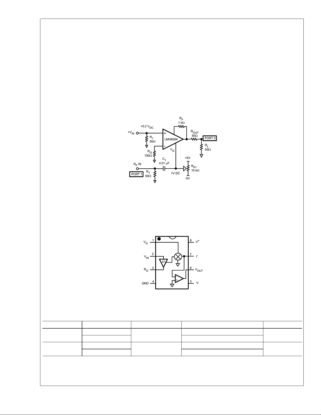
V
Typical Application
A
= 9.7 V/V
VMAX
Gain vs. V
LMH™is a trademark of National Semiconductor Corporation.
© 2004 National Semiconductor Corporation DS200843 www.national.com
G
20084311
20084302
Absolute Maximum Ratings (Note 1)
If Military/Aerospace specified devices are required,
please contact the National Semiconductor Sales Office/
LMH6504
Distributors for availability and specifications.
Junction Temperature 150˚C
Soldering Information:
Infrared or Convection (20 sec) 235˚C
Wave Soldering (10 sec) 260˚C
ESD Tolerance (Note 4):
Human Body 1000V
Machine Model 100V
±
Input Current
10 mA
Output Current 120 mA (Note 3)
Supply Voltages (V
Voltage at Input/ Output pins V
+-V−
) 12.6V
+
+0.8V, V−−0.8V
Storage Temperature Range −65˚C to 150˚C
Operating Ratings (Note 1)
Supply Voltages (V
Operating Temperature Range −40˚C to +85˚C
Thermal Resistance: (θ
8 -Pin SOIC 60 165
8-Pin MSOP 65 235
+-V−
) 7Vto12V
)(θJA)
JC
Electrical Characteristics(Note 2)
Unless otherwise specified, all limits guaranteed for TJ= 25˚C, VS=±5V, A
±
0.1V, RL= 100Ω,VG= +2V. Boldface limits apply at the temperature extremes.
Symbol Parameter Conditions
Frequency Domain Response
BW -3dB Bandwidth V
GF Gain Flatness V
<
1V
OUT
V
OUT
OUT
<
4VPP,A
<
1V
PP
= 100 58
VMAX
PP
0.9V ≤ VG≤ 2V,±0.2 dB
Att Range Flat Band (Relative to Max Gain)
Attenuation Range (Note 13)
BW
Gain control Bandwidth V
±
0.2 dB Flatness, f<30 MHz 26
±
0.1 dB Flatness, f<30 MHz 9.5
= 1V (Note 12) 150 MHz
G
Control
CT (dB) Feed-through V
= 0V, 30 MHz
G
(Output/Input)
GR Gain Adjustment Range f<10 MHz 80
<
f
30 MHz 73
Time Domain Response
t
r,tf
Rise and Fall Time 0.5V Step 2.1 ns
OS % Overshoot 20 %
SR Slew Rate (Note 5) 4V Step, Non Inverting 800
4V Step, Inverting 1500
Distortion & Noise Performance
HD2 2
nd
Harmonic Distortion 2VPP, 20 MHz −47
rd
Harmonic Distortion –55
THD Total Harmonic Distortion −45
En tot Total Equivalent Input Noise f
I
N
Input Noise Current f>1 MHz 2.6 pA/
>
1 MHz, R
SOURCE
=50Ω 4.4 nV/
DG Differential Gain f = 4.43 MHz, RL= 100Ω 0.45 %
DP Differential Phase 0.13 deg
= 9.7 V/V, RF=1kΩ,RG= 100Ω,VIN=
VMAX
Min
(Note 6)
Typ
(Note 6)
(Note 6) Units
150
40 MHz
−53 dB
Max
MHz
dB
dB
V/µs
dBcHD3 3
www.national.com 2
Electrical Characteristics(Note 2) (Continued)
Unless otherwise specified, all limits guaranteed for TJ= 25˚C, VS=±5V, A
±
0.1V, RL= 100Ω,VG= +2V. Boldface limits apply at the temperature extremes.
Symbol Parameter Conditions
DC & Miscellaneous Performance
GACCU Gain Accuracy
(See Application Note)
G Match Gain Matching
(See Application Note
V
= 2.0V 0
G
<
0.8V
V
G
0.8V
<
V
2V
G
= 2.0V —
<
<
V
2V — +2.8/−4.2
G
K Gain Multiplier
(See Application Notes)
V
NL Input Voltage Range RGOpen
IN
V
LR
IN
I
RG_MAX
I
BIAS
TC I
R
IN
C
IN
I
VG
TC I
R
VG
C
VG
V
OUT
V
OUT
R
OUT
I
OUT
V
O
OFFSET
RGCurrent Pin 3
Bias Current Pin 2 (Note 7) −1.4 −3.5
Bias Current Drift Pin 2 (Note 8) –190 pA/˚C
BIAS
Input Resistance Pin 2 7 MΩ
Input Capacitance Pin 2 2.8 pF
VGBias Current Pin 1, VG= 2V (Note 7) 0.9 µA
VGBias Drift Pin 1 (Note 8) 10 pA/˚C
VG
VGInput Resistance Pin 1 25 MΩ
VGInput Capacitance Pin 1 2.8 pF
L Output Voltage Range RL= 100Ω
NL RL= Open
Output Impedance DC 0.12 Ω
Output Current V
Output Offset Voltage 0V<V
+PSRR +Power Supply Rejection Ratio
(Note 9)
−PSRR −Power Supply Rejection Ratio
(Note 9)
I
S
Supply Current No Load 8.5
= 100Ω
G
=±4V from Rails
OUT
<
2V
G
Input Referred, 1V change,
= 2.2V
V
G
Input Referred, 1V change,
= 2.2V
V
G
= 9.7 V/V, RF=1kΩ,RG= 100Ω,VIN=
VMAX
Min
(Note 6)
0.920
0.916
±
±
±
±
±
±
±
±
–65 –76 dB
–65 –88
0.48
0.40
4.8
4.0
2.0
1.7
60
40
6.5
Typ
(Note 6)
±
0.33
Max
(Note 6) Units
±
0.45
±
3.9
±
0.42
0.965 1.01
1.02
±
3.2
±
0.68
±
6.8 mA
−3.7
±
2.2
±
3.1
±
80 mA
±
10
±
55
±
70
11 15
16
LMH6504
dB
dB
V/V
V
µA
V
mV
dB
mA
www.national.com3
Electrical Characteristics(Note 2) (Continued)
Note 1: Absolute Maximum Ratings indicate limits beyond which damage to the device may occur. Operating Ratings indicate conditions for which the device is
intended to be functional, but specific performance is not guaranteed. For guaranteed specifications, see the Electrical Characteristics.
LMH6504
Note 2: Electrical Table values apply only for factory testing conditions at the temperature indicated. Factory testing conditions result in very limited self-heating of
the device such that T
Note 3: The maximum output current (I
Note 4: Human body model, 1.5 kΩ in series with 100 pF. Machine Model, 0Ω in series with 200 pF
Note 5: Slew rate is the average of the rising and falling slew rates.
Note 6: Typical values represent the most likely parametric norm. Bold numbers refer to over temperature limits.
Note 7: Positive current corresponds to current flowing into the device.
Note 8: Drift determined by dividing the change in parameter distribution at temperature extremes by the total temperature change.
Note 9: +PSRR definition: [|∆V
subtracted out.
Note 10: Gain/Phase normalized to low frequency value at 25˚C.
Note 11: Gain/Phase normalized to low frequency value at each setting.
Note 12: Gain control frequency response schematic:
. No guarantee of parametric performance is indicated in the electrical tables under conditions of internal self-heating where T
J=TA
OUT
) is determined by device power dissipation limitations or value specified, whichever is lower.
OUT
/∆V+|/AV], −PSRR definition: [|∆V
/∆V−|/AV] with 0.1V input voltage. ∆V
OUT
is the change in output voltage with offset shift
OUT
>
TA.
J
20084316
Note 13: Flat Band Attenuation (Relative To Max Gain) Range Definition: Specified as the attenuation range from maximum which allows gain flatness specified
±
(either
0.2dB or±0.1dB), relative to A
±
0.2 dB: 19.7 dB down to -6.3 dB = 26 dB range
±
0.1 dB: 19.7 dB down to 10.2 dB = 9.5 dB range
gain. For example, for f<30 MHz, here are the Flat Band Attenuation ranges:
VMAX
Connection Diagram
8-Pin SOIC
Top View
20084301
Ordering Information
Package Part Number Package Marking Transport Media NSC Drawing
8-Pin SOIC LMH6504MA LMH6504MA 95 Units/Rail M08A
LMH6504MAX 2.5k Units Tape and Reel
8-Pin MSOP
LMH6504MM
LMH6504MMX 3.5k Units Tape and Reel
A93A
1k Units Tape and Reel
MUA08A
www.national.com 4
LMH6504
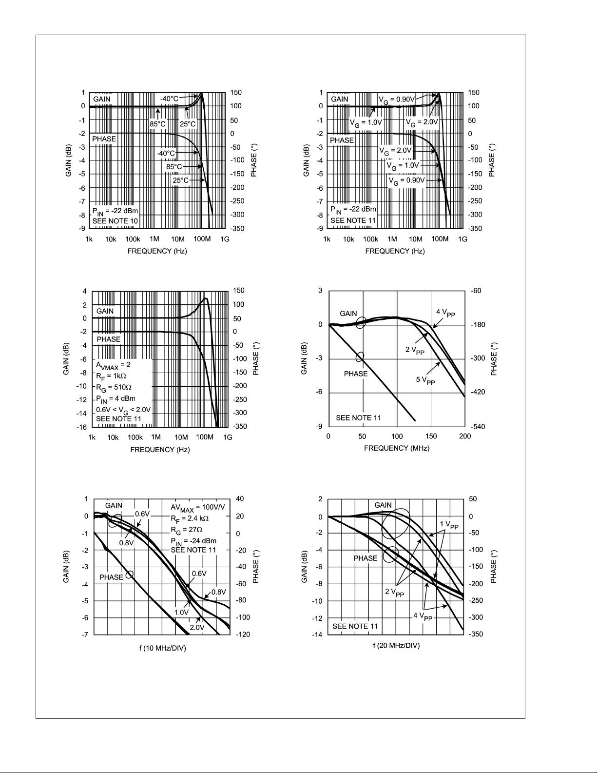
Typical Performance Characteristics Unless otherwise specified: V
V
G=VGMAX,RF
=1kΩ,RG= 100Ω,VIN= 0.1V, input terminated in 50Ω.RL= 100Ω, Typical values.
Frequency Response Over Temperature Frequency Response for Various V
20084303 20084304
Frequency Response (A
= 2) Inverting Frequency Response
VMAX
=±5V, TA= 25˚C,
S
G
Frequency Response for Various VG(A
(Large Signal) Frequency Response for Various Amplitudes
VMAX
20084346
= 100)
20084345
20084344
20084364
www.national.com5
Typical Performance Characteristics Unless otherwise specified: V
V
G=VGMAX,RF
LMH6504
=1kΩ,RG= 100Ω,VIN= 0.1V, input terminated in 50Ω.RL= 100Ω, Typical values. (Continued)
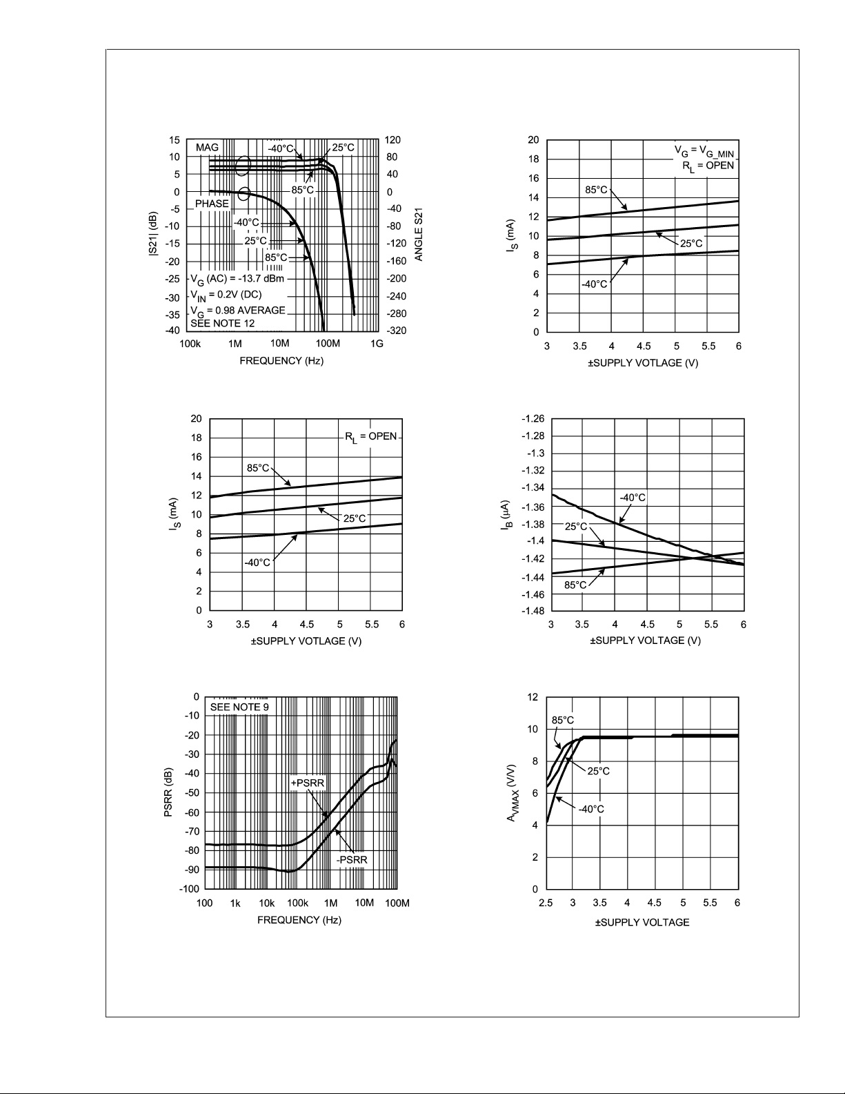
Gain Control Frequency Response I
=±5V, TA= 25˚C,
S
vs. V
S
S
20084333
ISvs. V
S
20084320
PSRR A
Input Bias Current vs. V
vs. Supply Voltage
VMAX
20084321
S
20084322
20084334
www.national.com 6
20084323
 Loading...