


查询LMH6503供应商
LMH6503
Wideband, Low Power, Linear Variable Gain Amplifier
LMH6503 Wideband, Low Power, Linear Variable Gain Amplifier
June 2004
General Description
The LMH™6503 is a wideband DC coupled differential input
voltage controlled gain stage followed by a high-speed current feedback Op Amp which can directly drive a low impedance load. Gain adjustment range is more than 70dB for up
to 10MHz.
Maximum gain is set by external components and the gain
can be reduced all the way to cut-off. Power consumption is
370mW with a speed of 135MHz . Output referred DC offset
voltage is less than 350mV over the entire gain control
voltage range. Device-to-device Gain matching is within
0.7dB at maximum gain. Furthermore, gain at any V
tested and the tolerance is guaranteed. The output current
feedback Op Amp allows high frequency large signals (Slew
Rate = 1800V/µs) and can also drive heavy load current
(75mA). Differential inputs allow common mode rejection in
low level amplification or in applications where signals are
carried over relatively long wires. For single ended operation, the unused input can easily be tied to ground (or to a
virtual half-supply in single supply application). Inverting or
non-inverting gains could be obtained by choosing one input
polarity or the other.
To further increase versatility when used in a single supply
application, gain control range is set to be from −1V to +1V
relative to pin 11 potential (ground pin). In single supply
operation, this ground pin is tied to a "virtual" half supply.
Gain control pin has high input impedance to simplify its
drive requirement. Gain control is linear in V/V throughout
the gain adjustment range. Maximum gain can be set to be
anywhere between 1V/V to 100V/V or higher. For linear in dB
gain control applications, see LMH6502 datasheet.
The LMH6503 is available in the SOIC-14 and TSSOP-14
package.
G
Features
VS=±5V, TA= 25˚C, RF=1kΩ,RG= 174Ω,RL= 100Ω,A
=A
n -3dB BW 135MHz
n Gain control BW 100MHz
n Adjustment range (typical over temp) 70dB
n Gain matching (limit)
n Slew rate 1800V/µs
n Supply current (no load) 37mA
n Linear output current
n Output voltage (R
is
n Input voltage noise 6.6nV/
n Input current noise 2.4pA/
n THD (20MHz, RL= 100Ω,VO=2VPP) −57dBc
n Replacement for CLC522
= 10, Typical values unless specified.
V(MAX)
= 100Ω)
L
Applications
n Variable attenuator
n AGC
n Voltage controller filter
n Multiplier
±
0.7dB
±
75mA
±
V
3.2V
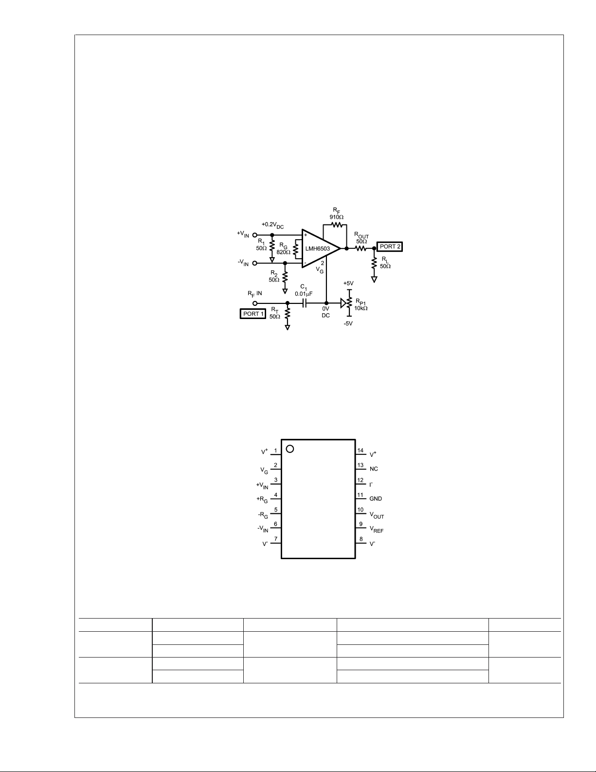
Typical Application
Gain vs. VGfor Various Temperature
LMH™is a trademark of National Semiconductor Corporation.
© 2004 National Semiconductor Corporation DS200739 www.national.com
20073913
A
VMAX
= 10V/V
20073933

Absolute Maximum Ratings (Note 1)
If Military/Aerospace specified devices are required,
please contact the National Semiconductor Sales Office/
LMH6503
Distributors for availability and specifications.
Infrared or Convection (20 sec) 235˚C
Wave Soldering (10 sec) 260˚C
Storage Temperature Range −65˚C to +150˚C
Junction Temperature +150˚C
ESD Tolerance: (Note 4)
Human Body 2KV
Machine Model 200V
±
Input Current
V
Differential
IN
10mA
±
(V+−V−)
Output Current 120mA (Note 3)
Supply Voltages (V
Voltage at Input/ Output pins V
+-V−
) 12.6V
+
+0.8V,V−- 0.8V
Operating Ratings (Note 1)
Supply Voltages (V
Temperature Range −40˚C to +85˚C
Thermal Resistance: θ
14-Pin SOIC 138˚C/W 45˚C/W
14-Pin TSSOP 160˚C/W 51˚C/W
+-V−
) 5Vto12V
JA
θ
Soldering Information:
Electrical Characteristics(Note 2)
Unless otherwise specified, all limits guaranteed for TJ= 25˚C, VS=±5V, A
=±0.1V, RL= 100Ω,VG= +1V. Boldface limits apply at the temperature extremes.
_DIFF
Symbol Parameter Conditions
Frequency Domain Response
BW -3dB Bandwidth V
GF Gain Flatness V
Att Range Flat Band (Relative to Max Gain)
Attenuation Range (Note 13)
BW
Gain Control Bandwidth V
<
0.5
OUT
V
OUT
OUT
−1V
±
0.2dB Flatness, f<30MHZ 20
±
0.1dB, f<30MHZ 6.6
G
PP
<
<
<
V
0.5PP,A
0.5VPP,
<
1V,±0.2dB
G
= 100 50
V(MAX)
= 0V (Note 11) 100 MHz
Control
PL Linear Phase Deviation DC to 60MHz 1.6 deg
G Delay Group Delay DC to 130MHz 2.6 ns
CT (dB) Feed-through V
= −1.2V, 30MHz (Output
G
Referred)
GR Gain Adjustment Range f<10MHz 79
<
f
30MHz 68
Time Domain Response
t
r,tf
Rise and Fall Time 0.5V Step 2.2 ns
OS% Overshoot 0.5V Step 10 %
SR Slew Rate 4V Step (Note 5) 1800 V/µs
∆G Rate Gain Change Rate V
= 0.3V, 10%−90% of final
IN
output
Distortion & Noise performance
HD2 2
HD3 3
THD Total Harmonic Distortion 2V
nd
Harmonic Distortion 2VPP, 20MHz −60 dBc
rd
Harmonic Distortion 2VPP, 20MHz −61 dBc
, 20MHz −57 dBc
PP
En tot Total Equivalent Input Noise 1MHz to 150MHz 6.6 nV/
I
n
Input Noise Current 1MHz to 150MHz 2.4 pA/
DG Differential Gain f = 4.43MHz, RL= 150Ω, Neg.
Sync
DP Differential Phase f = 4.43MHz, R
= 150Ω, Neg.
L
Sync
= 10, VCM= 0V, RF=1kΩ,RG= 174Ω,V
V(MAX)
Min
(Note 6)
Typ
(Note 6)
Max
(Note 6) Units
135
40 MHz
−48 dB
4.6 dB/ns
0.15 %
0.22 deg
JC
-
IN
MHz
MHz
dB
www.national.com 2
Electrical Characteristics(Note 2) (Continued)
Unless otherwise specified, all limits guaranteed for TJ= 25˚C, VS=±5V, A
=±0.1V, RL= 100Ω,VG= +1V. Boldface limits apply at the temperature extremes.
_DIFF
Symbol Parameter Conditions
DC & Miscellaneous Performance
GACCU Gain Accuracy (see Application
Notes)
G Match Gain Matching (see Application
Notes)
K Gain Multiplier (see Application
Notes)
V
CM
V
IN_ DIFF
I
RG MAX
I
BIAS
TC
BIAS
I
OFF
TC I
R
IN
C
IN
IV
G
TC IV
RV
CV
V
OUT
R
OUT
I
OUT
V
O
OFFSET
G
G
Input Voltage Range Pin3&6Common Mode,
Differential Input Voltage Across pins3&6
RGCurrent Pins4&5
Bias Current Pins3&6(Note 7) 11 18
Bias Current Drift Pin3&6(Note 8) 100 nA/˚C
Offset Current Pin3&6 0.01 2.0
Offset Current Drift (Note 8) 5 nA/˚C
OFF
Input Resistance Pin3&6 750 kΩ
Input Capacitance Pin3&6 5 pF
VGBias Current Pin 2, VG= 1.4V(Note 7) 45 µA
VGBias Drift Pin 2 (Note 8) 20 nA/˚C
G
VGInput Resistance Pin 2 70 KΩ
VGInput Capacitance Pin 2 1.3 pF
Output Voltage Range RL= 100Ω
Output Impedance DC 0.1 Ω
Output Current V
Output Offset Voltage −1V<V
+PSRR +Power Supply Rejection Ratio
(see (Note 10))
−PSRR −Power Supply Rejection Ratio
(see (Note 10))
CMRR Common Mode Rejection Ratio
(see (Note 9))
I
S
Supply Current RL= Open 37 50
V
=1.0V +0.25 +0.9/−0.4
G
<
<
V
1V
G
<
−0.7V
V
= 1.0 –
G
<
V
−0.7V
|CMRR|
<
V
1V
G
<
1V – +1.7/−1.1
G
<
<
V
1V – +4.0/−4.7
G
>
50dB (Note 9)
Pins3&6(Note 7),
=±2.5V
V
S
Open
R
L
±
4V from Rails
OUT
<
1V
G
Input Referred, 1V change,
VG= 1.4V
Input Referred, 1V change,
VG= 1.4V
Input Referred, V
<
−1.8V
R
V
CM
= Open, VS=±2.5V 12 20
L
<
G
1.8V
=1V
= 10, VCM= 0V, RF=1kΩ,RG= 174Ω,V
V(MAX)
Min
(Note 6)
Typ
(Note 6)
±
0.3 +1.3/−1.5
±
0.4 +4.4/−4.3
Max
(Note 6) Units
±
1.58
1.58
±
±
1.80
±
0.34
±
0.28
±
1.70
±
1.60
±
3.00
±
2.97
±
3.95
±
3.90
±
±
2.0
75
70
1.72 1.87
1.91
±
2.2 V
±
0.37
±
2.30 mA
310
±
3.20
±
4.05
±
90 mA
±
80
±
±
−80 −58
−56
−67 −57
−51
−67 dB
0.7
20
13
2.5
350
380
53
23
dB0V
dB0
V/V
V
µA
µA
V
mV
dB
dB
mA
-
IN
LMH6503
www.national.com3
Electrical Characteristics(Note 2) (Continued)
Note 1: Absolute Maximum Ratings indicate limits beyond which damage to the device may occur. Operating Ratings indicate conditions for which the device is
intended to be functional, but specific performance is not guaranteed. For guaranteed specifications, see the Electrical Characteristics tables.
LMH6503
Note 2: Electrical Table values apply only for factory testing conditions at the temperature indicated. Factory testing conditions result in very limited self-heating of
the device such that T
Note 3: The maximum output current (I
Note 4: Human body model: 1.5kΩ in series with 100pF. Machine model: 0Ω in series with 200pF.
Note 5: Slew Rate is the average of the rising and falling rates.
Note 6: Typical values represent the most likely parametric norm. Bold numbers refer to over temperature limits.
Note 7: Positive current correspondes to current flowing in the device.
Note 8: Drift determined by dividing the change in parameter distribution at temperature extremes by the total temperature change.
Note 9: CMRR definition: [|∆V
Note 10: +PSRR definition: [|∆V
offset shift subtracted out.
Note 11: Gain Control Frequency Response Schematic:
. No guarantee of parametric performance is indicated in the electrical tables under conditions of internal self-heating where T
J=TA
OUT
OUT
) is determined by device power dissipation limitations or value specified, whichever is lower.
OUT
/∆VCM|/AV] with 0.1V differential input voltage. ∆V
/∆V+|/AV], -PSRR definition: [|∆V
/∆V−|/AV] with 0.1V differential input voltage. ∆V
OUT
is the change in output voltage with offset shift subtracted out.
OUT
is the change in output voltage with
OUT
>
TA.
J
20073932
Note 12: Gain/Phase normalized to low frequency value at each AV.
Note 13: Flat Band Attenuation (Relative To Max Gain) Range Definition: Specified as the attenuation range from maximum which allows gain flatness specified
±
(either
0.2dB or±0.1dB), relative to A
±
0.2dB: 10V/V down to 1V/V=20dB range
±
0.1dB: 10V/V down to 4.7V/V=6.5dB range
gain. For example, for f<30MHz, here are the Flat Band Attenuation ranges:
VMAX
Connection Diagram
14-Pin SOIC/TSSOP
Top View
20073946
Ordering Information
Package Part Number Package Marking Transport Media NSC Drawing
14-pin SOIC LMH6503MA LMH6503MA 55 Units/Rail M14A
LMH6503MAX 2.5k Units Tape and Reel
14-Pin TSSOP
LMH6503MT
LMH6503MTX 2.5k Units Tape and Reel
LMH6503MT
www.national.com 4
94 Units/Rail
MTC14

LMH6503
Typical Performance Charateristics Unless otherwise specified: V
=±5V, 25˚C, VG=V
S
G_MAX,VCM
= 0V, RF=1kΩ,RG= 174Ω, both inputs terminated in 50Ω,RL= 100Ω, Typical values, results referred to device output:
Small Signal Frequency Response (A
Frequency Response over Temperature (AV= 10) Frequency Response for Various VG(A
= 2) Large Signal Frequency Response (AV=2)
V
20073917 20073916
= 10)
VMAX
Frequency Response for Various VG(A
±
2.5V) Small Signal Frequency Response
(
20073919 20073920
= 10)
VMAX
20073930
20073914
www.national.com5

Typical Performance Charateristics Unless otherwise specified: V
=±5V, 25˚C, VG=V
S
= 0V, RF=1kΩ,RG= 174Ω, both inputs terminated in 50Ω,RL= 100Ω, Typical values, results referred to device
output: (Continued)
LMH6503
G_MAX,VCM
Large Signal Frequency Response
Frequency Response for Various VG(A
(Large Signal) Gain Control Frequency Response
VMAX
20073915
= 100)
Frequency Response for Various V
(Small Signal)
G(AVMAX
= 100)
20073943
20073944
ISvs. V
S
20073964 20073965
www.national.com 6
ISvs. V
20073928
S

LMH6503
Typical Performance Charateristics Unless otherwise specified: V
=±5V, 25˚C, VG=V
S
= 0V, RF=1kΩ,RG= 174Ω, both inputs terminated in 50Ω,RL= 100Ω, Typical values, results referred to device
output: (Continued)
Input Bias Current vs. V
S
20073966
A
VMAX
vs. V
S
PSRR±5V PSRR±2.5V
G_MAX,VCM
20073967
20073906
CMRR±5V CMRR±2.5V
20073904 20073905
20073907
www.national.com7

Typical Performance Charateristics Unless otherwise specified: V
=±5V, 25˚C, VG=V
S
= 0V, RF=1kΩ,RG= 174Ω, both inputs terminated in 50Ω,RL= 100Ω, Typical values, results referred to device
output: (Continued)
LMH6503
A
VMAX
vs. V
CM
A
VMAX
vs. V
G_MAX,VCM
CM
20073972
CM
20073974
Supply Current vs. V
CM
20073971
Supply Current vs. V
20073973
Output Offset Voltage vs.VCM(Typical Unit 1) Output Offset Voltage vs.VCM(Typical Unit 2)
20073975
www.national.com 8
20073976

LMH6503
Typical Performance Charateristics Unless otherwise specified: V
=±5V, 25˚C, VG=V
S
= 0V, RF=1kΩ,RG= 174Ω, both inputs terminated in 50Ω,RL= 100Ω, Typical values, results referred to device
output: (Continued)
Output Offset Voltage vs.V
(Typical Unit 3) Feed through Isolation
CM
20073977
Gain Flatness and Linear Phase Deviation Gain Flatness Frequency vs. Gain (Note 13)
G_MAX,VCM
20073918
20073921
Group Delay vs. Frequency K Factor vs. R
20073927
20073924
G
20073901
www.national.com9

Typical Performance Charateristics Unless otherwise specified: V
=±5V, 25˚C, VG=V
S
= 0V, RF=1kΩ,RG= 174Ω, both inputs terminated in 50Ω,RL= 100Ω, Typical values, results referred to device
output: (Continued)
LMH6503
G_MAX,VCM
Gain vs. V
Including Limits BW vs. RFfor Various R
G
20073912
Gain vs. VG(±5V) Output Offset Voltage vs. VG(Typical Unit 1)
G
20073903
20073913
Output Offset Voltage vs. VG(Typical Unit 2) Output Offset Voltage vs. VG(Typical Unit 3)
20073969
www.national.com 10
20073968
20073970

LMH6503
Typical Performance Charateristics Unless otherwise specified: V
=±5V, 25˚C, VG=V
S
= 0V, RF=1kΩ,RG= 174Ω, both inputs terminated in 50Ω,RL= 100Ω, Typical values, results referred to device
output: (Continued)
Output Offset Voltage vs.
±
VSfor Various V
(Typical Unit 1)
20073978
Output Offset Voltage vs.±VSfor Various V
G
Output Offset Voltage vs.
(Typical Unit 2)
G
±
VSfor Various V
(Typical Unit 3) Gain vs. VG(±2.5V)
G_MAX,VCM
G
20073979
Noise vs. Frequency (A
20073980
= 2) Noise vs. Frequency (A
VMAX
20073923 20073922
VMAX
20073929
= 10)
www.national.com11

Typical Performance Charateristics Unless otherwise specified: V
=±5V, 25˚C, VG=V
S
= 0V, RF=1kΩ,RG= 174Ω, both inputs terminated in 50Ω,RL= 100Ω, Typical values, results referred to device
output: (Continued)
LMH6503
G_MAX,VCM
Noise vs. Frequency (A
= 100) −1dB Compression
VMAX
20073931
Output Voltage vs. Output Current HD2 vs. P
20073911
OUT
20073945
HD3 vs. P
OUT
20073941
www.national.com 12
THD vs. P
20073940
OUT
20073939

LMH6503
Typical Performance Charateristics Unless otherwise specified: V
=±5V, 25˚C, VG=V
S
= 0V, RF=1kΩ,RG= 174Ω, both inputs terminated in 50Ω,RL= 100Ω, Typical values, results referred to device
output: (Continued)
HD2 & HD3 vs. V
G
VGBias Current vs. V
20073942 20073938
G
THD vs. V
G
Step Response Plot
G_MAX,VCM
20073937
Step Response Plot Gain vs. VGStep
20073963
20073962
20073981
www.national.com13

Typical Performance Charateristics Unless otherwise specified: V
=±5V, 25˚C, VG=V
S
= 0V, RF=1kΩ,RG= 174Ω, both inputs terminated in 50Ω,RL= 100Ω, Typical values, results referred to device
output: (Continued)
LMH6503
V
Feedthrough
G
20073982
Application Information
G_MAX,VCM
THEORY OF OPERATION
The LMH6503 is a linear wideband variable-gain amplifier as
illustrated in Figure 1. A voltage input signal may be applied
differentially between the two inputs (+V
,−VIN), or single-
IN
endedly by grounding one of the two unused inputs. The
LMH6503 input buffers convert the input voltage to a current
) that is a function of the differential input voltage (V
(I
RG
INPUT
= (+VIN) - (−VIN)) and the value of the gain setting resistor
). This current (IRG) is then mirrored to a gain stage with
(R
G
a current gain of K (1.72 nominal). The voltage controlled
two-quadrant multiplier attenuates this current which is then
converted to a voltage via the output amplifier. This output
amplifier is a current feedback op amp configured as a
Transimpedance amplifier. Its Transimpedance gain is the
feedback resistor (R
). The input signal, output, and gain
F
control are all voltages. The output voltage can easily be
calculated as shown in Equation 1:
(1)
Where K = 1.72 (Nominal)
since:
(3)
Notice also that Equation 3 holds for both differential and
single ended operation.
20073951
FIGURE 1. LMH6503 Functional Block Diagram
CHOOSING R
RGis calculated from Equation 4. V
AND R
F
G
INPUTMAX
is the maxi-
mum peak
The gain of the LMH6503 is therefore a function of three
external variables: R
, and VGas expressed in Equation
G,RF
2:
(2)
The gain control voltage (V
<
<
V
+1V. At VG= +1V, the gain of the LMH6503 is at its
G
) has an ideal input range of −1V
G
maximum as expressed in Equation 3:
www.national.com 14
input voltage (V
) determined by the application. I
pk
the maximum allowable current through R
2.3mA. Once A
and desired output voltages, R
Equation 5. These values of R
is determined from the minimum input
VMAX
is then determined using
F
and RGare
F
RGMAX
and is typically
G
(4)
is

LMH6503
Application Information (Continued)
(5)
the minimum possible values that meet the input voltage and
maximum gain constraints. Scaling the resistor values will
decrease bandwidth and improve stability.
Figure 2 illustrates the resulting LMH6503 bandwidths as a
function of the maximum ( y axis) and minimum (related to x
axis) input voltages when V
is held constant at 1VPP.
OUT
Once this is accomplished, the offset errors introduced by
the input stage and multiplier core can then be treated. The
second step requires the absence of an input signal and
matched source impedances on the two input pins in order to
cancel the bias current errors. This done, then +1.1V should
be applied to V
and the trim pot located at R10adjusted in
G
order to null the offset voltage seen at the LMH6503’s output.
If a more limited gain range is anticipated, the above adjustments should be made at these operating points. These
steps will minimize the output offset voltage. However, since
the offset term itself varies with the gain setting, the correction is not perfect and some residual output offset will remain.
GAIN ACCURACY
Defined as the ratio of measured gain (V/V), at a certain V
to the best fit line drawn through the typical gain (V/V)
<
<
V
distribution for −1V
(See Figure 4). The best fit gain (A
(V/V) = 4.87VG+ 4.61 (6)
A
V
ForaV
For: −1V ≤ V
range, the value specified in the tables represents
G
G
1V (results expressed in dB)
G
) is given by:
V
≤ +1V,RF=1kΩ,RG= 174Ω
the worst case accuracy over the entire range. The "Typical"
value would be the worst case ratio between the "Typical
Gain" and the best fit line. The "Max" value would be the
worst case between the max/min gain limit and the best fit
line.
,
G
20073902
FIGURE 2. Bandwidth vs. V
INMAX
and A
VMAX
ADJUSTING OFFSETS
Treating the offsets introduced by the input and output
stages of the LMH6503 is accomplished with a two step
process. The offset voltage of the output stage is treated by
first applying −1.1V on V
, which effectively isolates the
G
input stage and multiplier core from the output stage. As
illustrated in Figure 3, the trim pot located at R14 on the
LMH6503 Evaluation Board (CLC730033) should then be
adjusted in order to null the offset voltage seen at the
LMH6503’s output (pin 10).
GAIN MATCHING
Defined as the limit on gain variation at a certain V
(ex-
G
pressed in dB) (See Figure 4). Specified as "Max" only (no
"Typical"). For a V
range, the value specified represents the
G
worst case matching over the entire range. The "Max" value
would be the worst case ratio between the max/min gain limit
and the typical gain.
FIGURE 3. Nulling the Output Offset Voltage
20073955
FIGURE 4. Gain Accuracy and Gain Matching
Parameters Defined
20073954
www.national.com15

Application Information (Continued)
NOISE
LMH6503
Figure 5 describes the LMH6503’s output-referred spot
noise density as a function of frequency with A
The plot includes all the noise contributing terms. However,
with both inputs terminated in 50Ω, the input noise contribution is minimal. At A
flat-band input-referred spot noise density (e
. For applications with −3dB BW extending well into the
flat-band region, the input RMS voltage noise can be determined from the following single-pole model:
= 10V/V, the LMH6503 has a typical
VMAX
= 10V/V.
VMAX
) of 6.6nV/
in
(7)
required of the layout. Minimizing the parasitic capacitances
at pins 3, 4, 5, 6, 9, 10 and 12 will assure best high frequency
performance. The parasitic inductance of component leads
or traces to pins 4, 5 and 9 should also be kept to a
minimum. Parasitic or load capacitance, C
, on the output
L
(pin 10) degrades phase margin and can lead to frequency
response peaking or circuit oscillation. The LMH6503 is fully
stable when driving a 100Ω load. With reduced load (e.g.
1kΩ) there is a possibility of instability at very high frequencies beyond 400MHz especially with a capacitive load.
When the LMH6503 is connected to a light load as such, it is
recommended to add a snubber network to the output (e.g.
100Ω and 39pF in series tied between the LMH6503 output
and ground). C
can also be isolated from the output by
L
placing a small resistor in series with the output (pin 10).
Component parasitics also influence high frequency results.
Therefore it is recommended to use metal film resistors such
as RN55D or leadless components such as surface mount
devices. High profile sockets are not recommended.
National Semiconductor suggests the following evaluation
board as a guide for high frequency layout and as an aid in
device testing and characterization:
Device Package Evaluation Board Part
Number
LMH6503MA SOIC-14 CLC730033
LMH6503MT TSSOP-14 CLC730146
20073922
FIGURE 5. Output Referred Voltage Noise vs.
Frequency
CIRCUIT LAYOUT CONSIDERATIONS
Good high-frequency operation requires all of the decoupling capacitors shown in Figure 6 to be placed as close
as possible to the power supply pins in order to insure a
proper high-frequency low-impedance bypass. Adequate
ground plane and low inductive power returns are also
The evaluation board is shipped when a device sample
request is placed with National Semiconductor.
SINGLE SUPPLY OPERATION
It is possible to operate the LMH6503 with a single supply. To
do so, tie pin 11 (GND) to a potential about mid point
between V
+
and V−. Two examples are shown in Figure 7 &
Figure 8.
20073957
FIGURE 6. Required Power Supply Decoupling
www.national.com 16
20073935
FIGURE 7. AC Coupled Single Supply VGA

Application Information (Continued)
FIGURE 8. Transformer Coupled Single Supply VGA
20073936
Figure 10 plots to make sure the region of operation is not
overly restricted by the "pinching" of V
curves.
_MAX
G_LIMIT
, and V
c) "Max_gain" reduces. There is an intrinsic reduction in
max gain when the total supply voltage is reduced (see
Typical Performance Characteristics plots for Gain vs. V
(VS=±2.5V). In addition, there is the more drastic
mechanism described in "b" above and shown in Figure
9.
+
Similar plots for V
= 5V operation are shown in Figure 10 for
comparison and reference.
LMH6503
-
G
G
OPERATING AT LOWER SUPPLY VOLTAGES
The LMH6503 is rated for operation down to 5V supplies (V
-V−). There are some specifications shown for operation at
±
2.5V within the data sheet (i.e. Frequency Response,
CMRR, PSRR, Gain vs. V
, etc.). Compared to±5V opera-
G
tion, at lower supplies:
a) V
range constricts. Referring to Figure 9, note that
G
V
G_MAX(VG
0.5V (V
same time, gain cut-off (V
- 1V with V
voltage required to get maximum gain) is
=±2.5V) compared to 1.0V for VS=±5V. At the
S
=±5V.
S
) would shift to −0.5V from
G_MIN
Table 1 shows the approximate expressions for various
voltages as a function of V-:
V
G
−
−0.2 x V
−
−
b) V
V
V
G_MIN
V
G_MID
V
G_MAX
G_LIMIT
Table 1: V
G
Definition Based on V
G
Definition Expression (V)
Gain Cut-off 0.2 x V
A
/2 0
VMAX
A
VMAX
(maximum permissible voltage on VG)isreduced. This is due to limitations within the device arising
from transistor headroom. Beyond this limit, device performance will be affected (non-destructive). Referring to
Figure 9, note that with V
is approaching V
+
= 2.5V, and V−= −4V, V
and already "Max gain" is re-
G_MAX
G_LIMIT
duced by 1dB. This means that operating under these
conditions has reduced the maximum permissible voltage
to a level below what is needed to get Max gain. If
on V
G
supply voltages are asymmetrical, reference Figure 9 and
+
20073926
FIGURE 9. V
G_MAX,VG_LIMIT
, & Max-gain vs. V
-
(V+= 2.5V)
20073925
FIGURE 10. V
G_MAX,VG_LIMIT
, & Max-gain vs. V
-
(V+= 5V)
www.national.com17

Application Circuits
FOUR-QUADRANT MULTIPLIER
LMH6503
Applications requiring multiplication, squaring or other nonlinear functions can be implemented with four-quadrant multipliers. The LMH6503 implements a four-quadrant multiplier
as illustrated in Figure 11:
FIGURE 11. Four Quadrant Multiplier
20073958
nd
2
ORDER TUNABLE BANDPASS FILTER
The LMH6503 Variable-Gain Amplifier placed into a feedback loop provides signal processing function such as in a
2nd order tunable bandpass filter. The center frequency of
the 2nd order bandpass shown in Figure 13 is adjusted
through the use of the LMH6503’s gain control voltage, V
The integrators implemented with two sections of a
LMH6682, provide the coefficients for the transfer function.
.
G
FREQUENCY SHAPING
Frequency shaping and bandwidth extension of the
LMH6503 can be accomplished using parallel networks connected across the R
ports. The network shown in the
G
Figure 12 schematic will effectively extend the LMH6503’s
bandwidth.
20073959
FIGURE 12. Frequency Shaping
20073960
20073961
FIGURE 13. Tunable Bandpass Filter
www.national.com 18

Physical Dimensions inches (millimeters) unless otherwise noted
LMH6503
14-Pin SOIC
NS Package Number M14A
14-Pin TSSOP
NS Package Number MTC14
www.national.com19

Notes
LMH6503 Wideband, Low Power, Linear Variable Gain Amplifier
LIFE SUPPORT POLICY
NATIONAL’S PRODUCTS ARE NOT AUTHORIZED FOR USE AS CRITICAL COMPONENTS IN LIFE SUPPORT
DEVICES OR SYSTEMS WITHOUT THE EXPRESS WRITTEN APPROVAL OF THE PRESIDENT AND GENERAL
COUNSEL OF NATIONAL SEMICONDUCTOR CORPORATION. As used herein:
1. Life support devices or systems are devices or
systems which, (a) are intended for surgical implant
into the body, or (b) support or sustain life, and
whose failure to perform when properly used in
accordance with instructions for use provided in the
labeling, can be reasonably expected to result in a
significant injury to the user.
BANNED SUBSTANCE COMPLIANCE
National Semiconductor certifies that the products and packing materials meet the provisions of the Customer Products
Stewardship Specification (CSP-9-111C2) and the Banned Substances and Materials of Interest Specification
(CSP-9-111S2) and contain no ‘‘Banned Substances’’ as defined in CSP-9-111S2.
National Semiconductor
Americas Customer
Support Center
Email: new.feedback@nsc.com
Tel: 1-800-272-9959
www.national.com
National does not assume any responsibility for use of any circuitry described, no circuit patent licenses are implied and National reserves the right at any time without notice to change said circuitry and specifications.
National Semiconductor
Europe Customer Support Center
Fax: +49 (0) 180-530 85 86
Email: europe.support@nsc.com
Deutsch Tel: +49 (0) 69 9508 6208
English Tel: +44 (0) 870 24 0 2171
Français Tel: +33 (0) 1 41 91 8790
2. A critical component is any component of a life
support device or system whose failure to perform
can be reasonably expected to cause the failure of
the life support device or system, or to affect its
safety or effectiveness.
National Semiconductor
Asia Pacific Customer
Support Center
Email: ap.support@nsc.com
National Semiconductor
Japan Customer Support Center
Fax: 81-3-5639-7507
Email: jpn.feedback@nsc.com
Tel: 81-3-5639-7560
 Loading...