LMH2180
75 MHz Dual Clock Buffer
LMH2180 75 MHz Dual Clock Buffer
January 24, 2008
General Description
The LMH2180 is a high speed dual clock buffer designed for
portable communications and applications requiring multiple
accurate multi-clock systems. The LMH2180 integrates two
75 MHz low noise buffers with independent shutdown pins
into a small package. The LMH2180 ensures superb system
operation between the baseband and the oscillator signal
path by eliminating crosstalk between the multiple clock signals.
Unique technology and design provides the LMH2180 with
the ability to accurately drive both large capacitive and resistive loads. Low supply current combined with shutdown pins
for each channel means the LMH2180 is ideal for battery
powered applications. The LMH2180's rapid recovery after
disable optimizes performance and current consumption.
This part does not use an internal ground reference, thus providing additional system flexibility. The LMH2180 operates
both with single and split supplies.
The flexible buffers provide system designers the capacity to
manage complex clock signals in the latest wireless applications. Each buffer delivers 106 V/μs internal slew rate with
independent shutdown and duty cycle precision. The patented analog circuit of each buffer drives capacitive loads greater
than 20 pF. Each input is internally biased to 1V, removing
the need for external resistors. Both channels have rail-to-rail
inputs and outputs, a gain of one, and are AC coupled with
the use of one capacitor.
Replacing a discrete buffer solution with the LMH2180 provides many benefits: simplified board layout, minimized parasitic components, simplified BOM, design durability across
multiple applications, simplification of clock paths, and the
ability to reduce the number of clock signal generators in the
system. The LMH2180 is produced in the tiny 8-pin LLP solder
bump and no pullback packages minimizing the required PCB
space. National’s advanced packaging offers direct PCB-IC
evaluation via pin access.
Features
(Typical values are: V
otherwise specified.)
Small signal bandwidth 78 MHz
■
Supply voltage range 2.4V to 5V
■
Phase noise (VIN = 1 VPP,
■
fC = 38.4 MHz, Δf = 1kHz)
Slew rate 106 V/μs
■
Total supply current 2.3 mA
■
Shutdown current 30 µA
■
Rail-to-rail input and output
■
Individual buffer enable pins
■
Rapid Ton technology
■
Crosstalk rejection circuitry
■
8-pin LLP, pin access packaging
■
Temperature range −40°C to 85°C
■
= 2.7V and CL = 10 pF, unless
SUPPLY
-123dBc/Hz
Applications
3G mobile applications
■
WLAN–WiMAX modules
■
TD_SCDMA multi-mode MP3 and camera
■
GSM modules
■
Oscillator modules
■
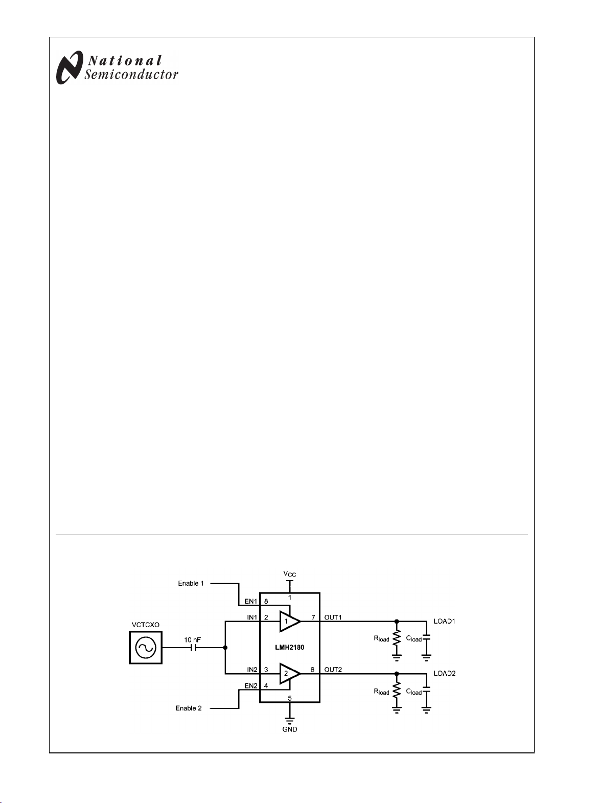
Typical Application
30024602
© 2008 National Semiconductor Corporation 300246 www.national.com
Absolute Maximum Ratings (Note 1)
If Military/Aerospace specified devices are required,
please contact the National Semiconductor Sales Office/
LMH2180
Distributors for availability and specifications.
Supply Voltages (V+– V−) 5.5V
ESD Tolerance
Human Body (Note 4) 2000V
Machine Model (Note 5) 200V
Charged Device Model 1000V
Junction Temperature (Note 3) +150°C
Soldering Information
Infrared or Convection (35 sec.) 235°C
Operating Ratings (Note 1)
Supply Voltage (V+ – V−)
Temperature Range (Notes 2, 3) −40°C to +85°C
Package Thermal Resistance (Notes 2, 3)
LLP-8 (θJA)
2.4V to 5.0V
217°C/W
Storage Temperature Range −65°C to +150°C
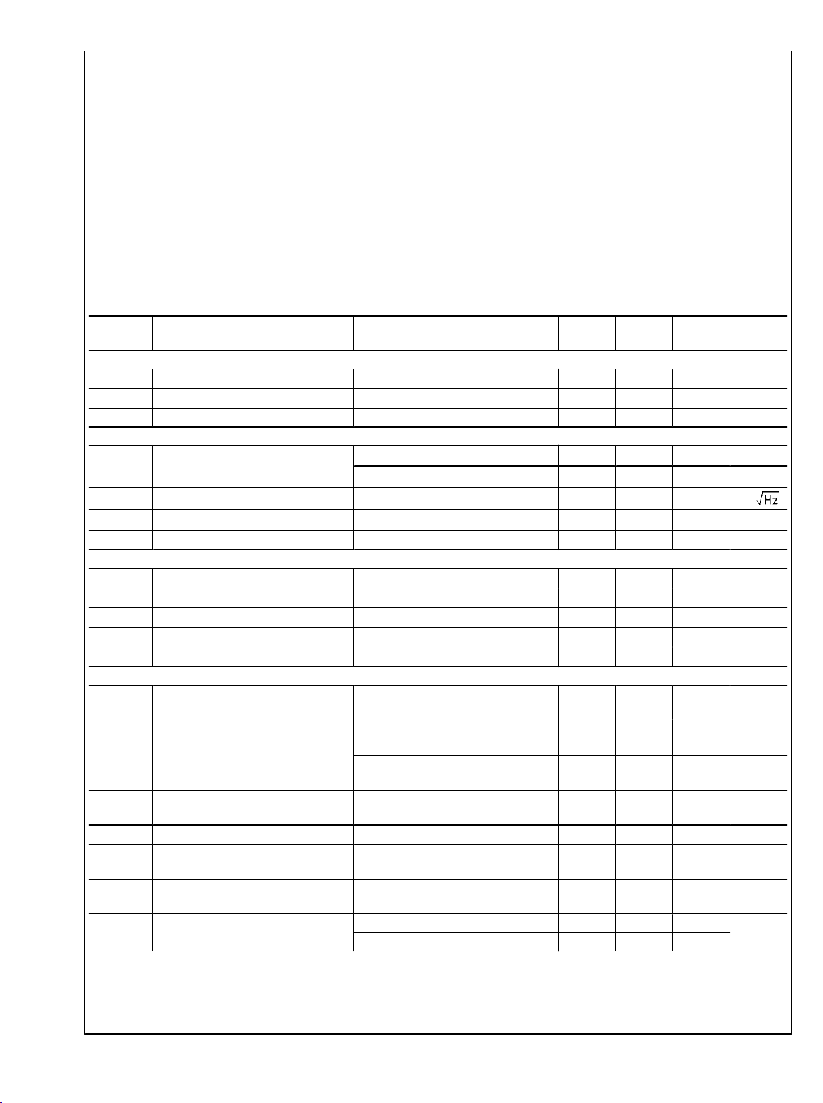
2.7V Electrical Characteristics
Unless otherwise specified, all limits are guaranteed for TJ = 25°C, VDD = 2.7V, VSS = 0V, VCM = 1V, Enable
RL = 30 kΩ, Load is connected to VSS, C
COUPLING
= 10 nF. Boldface limits apply at temperature range extremes of operating
condition. See (Note 2)
Symbol Parameter Conditions Min
(Note 7)
(Note 6)
Frequency Domain Response
SSBW Small Signal Bandwidth VIN = 100 mVPP; −3 dB
LSBW Large Signal Bandwidth VIN = 1.0 VPP; −3 dB
78 MHz
60 MHz
GFN Gain Flatness < 0.1 dB f > 100 kHz 4.9 MHz
Distortion and Noise Performance
φ
n
Phase Noise
VIN = 1 VPP, fC = 38.4 MHz, Δf = 1 kHz
VIN = 1 VPP, fC = 38.4 MHz, Δf = 10 kHz
e
n
I
SOLATION
Input-Referred Voltage Noise
Output to Input
f = 1 MHz, R
f = 1 MHz, R
SOURCE
SOURCE
= 50Ω
= 50Ω
CT Crosstalk Rejection f = 38.4 MHz, VIN = 1 V
PP
−123 dBc/Hz
−132 dBc/Hz
13
84 dB
41 dB
Time Domain Response
t
r
t
f
t
s
OS Overshoot 0.1 VPP Step
SR Slew Rate (Note 8) VIN = 2 V
Rise Time 0.1 VPP Step (10-90%)
Fall Time
Settling Time to 0.1% 1 VPP Step
PP
6 ns
5 ns
120 ns
37 %
106 V/µs
Static DC Performance
I
S
Supply Current Enable
Enable1 = VDD , Enable2 = VSS , No
Load
Enable
= VDD ; No Load
1,2
= VSS ; No Load
1,2
2.3
1.3
30
PSRR Power Supply Rejection Ratio DC (3.0V to 5.0V) 65
64
A
CL
V
OS
TC V
R
OUT
Small Signal Voltage Gain VIN = 0.2 V
Output Offset Voltage
Temperature Coefficient Output
OS
Offset Voltage (Note 9)
PP
0.95 1.0 1.05 V/V
-0.5
2.8 µV/°C
Output Resistance f = 100 kHz 0.6
f = 38.4 MHz 166
= VDD, CL = 10 pF,
1,2
Typ
Max
(Note 7)
2.7
2.9
1.5
1.6
41
46
68 dB
17
18
Units
nV/
mA
mA
μA
mV
Ω
www.national.com 2
LMH2180
Symbol Parameter Conditions Min
(Note 7)
Typ
(Note 6)
Max
(Note 7)
Units
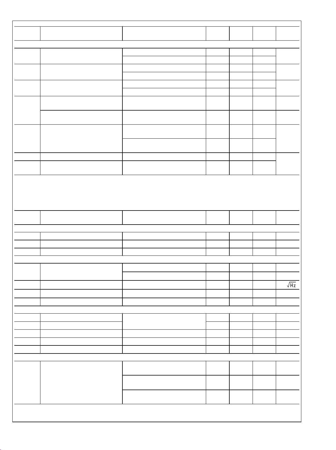
Miscellaneous Performance
R
IN
C
IN
Z
IN
V
O
I
SC
V
en_hmin
V
en_lmax
Input Resistance per Buffer Enable = V
Enable = V
Input Capacitance per Buffer Enable = V
Enable = V
Input Impedance f = 38.4 MHz, Enable = V
f = 38.4 MHz, Enable = V
Output Swing Positive VIN = V
DD
DD
SS
DD
SS
DD
SS
2.66
2.65
Output Swing Negative VIN = V
Output Short-Circuit Current
(Notes 10, 11)
SS
Sourcing, VIN = VDD, V
Sinking, VIN = VSS, V
OUT
OUT
= V
= V
DD
SS
−21
−18
Enable High Active Minimum Voltage
Enable Low Inactive Maximum
Voltage
137
137
1.3
1.3
4.5
4.2
2.69
19
−25
23
15
25
1.2
0.6
35
37
kΩ
pF
kΩ
V
mV
mA
V
5V Electrical Characteristics
Unless otherwise specified, all limits are guaranteed for TJ = 25°C, VDD = 5V, VSS = 0V, VCM = 1V, Enable
RL = 30 kΩ, Load is connected to VSS, C
COUPLING
= 10 nF. Boldface limits apply at temperature range extremes of operating
condition. See (Note 2)
Symbol Parameter Conditions Min
(Note 7)
(Note 6)
Frequency Domain Response
SSBW Small Signal Bandwidth VIN = 100 mVPP; −3 dB 87 MHz
LSBW Large Signal Bandwidth VIN = 1.0 VPP; −3 dB 68 MHz
GFN Gain Flatness < 0.1 dB f > 100 kHz 25 MHz
Distortion and Noise Performance
φ
n
e
n
I
SOLATION
Phase Noise
Input-Referred Voltage Noise
Output to Input
VIN = 1 VPP, fC = 38.4 MHz, Δf = 1 kHz
VIN = 1 VPP, fC = 38.4 MHz, Δf = 10 kHz
f = 1 MHz, R
f = 1 MHz, R
SOURCE
SOURCE
= 50Ω
= 50Ω
12
84 dB
CT Crosstalk Rejection f = 38.4 MHz, PIN = 0 dBm 59 dB
Time Domain Response
t
r
t
f
t
s
Rise Time 0.1 VPP Step (10-90%) 6 ns
Fall Time 6 ns
Settling Time to 0.1% 1 VPP Step 70 ns
OS Overshoot 0.1VPP Step 13 %
SR Slew Rate (Note 8) VIN = 2 V
PP
124 V/µs
Static DC Performance
I
S
Supply Current Enable
Enable1 = VDD, Enable2 = VSS ; No
Load
Enable
= VDD ; No Load
1,2
= VSS ; No Load
1,2
3.4
1.8
32
= VDD, CL = 10 pF,
1,2
Typ
(Note 7)
−123
−132
Max
4.0
4.1
2.2
2.3
43
49
Units
dBc/Hz
dBc/Hz
nV/
mA
mA
μA
3 www.national.com
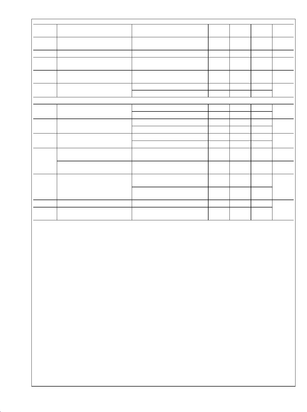
Symbol Parameter Conditions Min
PSRR Power Supply Rejection Ratio DC (3.0V to 5.0V) 65
LMH2180
A
CL
V
OS
TC V
Small Signal Voltage Gain VIN = 0.2 V
Output Offset Voltage
Temperature Coefficient Output
OS
PP
Offset Voltage (Note 9)
R
OUT
Output Resistance f = 100 kHz 0.5
f = 38.4 MHz 126
Miscellaneous Performance
R
IN
C
IN
Z
IN
V
O
I
SC
Input Resistance per Buffer Enable = V
Enable = V
Input Capacitance per Buffer Enable = V
Enable = V
DD
SS
DD
SS
Input Impedance f = 38.4 MHz, Enable = V
f = 38.4 MHz, Enable = V
Output Swing Positive VIN = V
Output Swing Negative VIN = V
Output Short-Circuit Current
DD
SS
Sourcing, VIN = VDD, V
OUT
DD
SS
= V
SS
(Notes 10, 11)
V
en_hmin
V
en_lmax
Enable High Active Minimum Voltage
Enable Low Inactive Maximum
Sinking, VIN = VSS, V
OUT
= V
DD
Voltage
(Note 7)
64
Typ
(Note 6)
68 dB
Max
(Note 7)
0.95 1.0 1.05 V/V
−1.4
21
22
2.4 µV/°C
138
138
1.3
1.3
4.3
4.2
4.96
4.95
−80
−62
60
43
1.2
4.99
10
−90
65
35
50
0.6
Units
mV
Ω
kΩ
pF
kΩ
V
mV
mA
V
Note 1: “Absolute Maximum Ratings” indicate limits beyond which damage to the device may occur, including inoperability and degradation of the device reliability
and/or performance. Functional operation of the device and/or non-degradation at the Absolute Maximum Ratings or other conditions beyond those indicated in
the Recommended Operating Conditions is not implied. The Recommended Operating Conditions indicate conditions at which the device is functional and the
device should not be operated beyond such conditions. All voltages are measured with respect to the ground pin, unless otherwise specified.
Note 2: The Electrical Characteristics tables list guaranteed specifications under the listed Recommended Operating Conditions except as otherwise modified
or specified by the Electrical Characteristics Conditions and/or Notes. Typical specifications are estimations only and are not guaranteed.
Note 3: The maximum power dissipation must be derated at elevated temperatures and is dictated by T
allowable power dissipation is P
Note 4: Human body model, applicable std. JESD22–A114C.
Note 5: Machine model, applicable std. JESD22–A115–A.
Note 6: Typical values represent the most likely parametric norms at TA = +25°C, and at the Recommended Operation Conditions at the time of product
characterization and are not guaranteed.
Note 7: Datasheet min/max specification limits are guaranteed by test or statistical analysis.
Note 8: Slew rate is the average of the rising and falling slew rates.
Note 9: Average Temperature Coefficient is determined by dividing the changing in a parameter at temperature extremes by the total temperature change.
Note 10: Short−Circuit test is a momentary test. Continuous short circuit operation at elevated ambient temperature can result in exceeding the maximum allowed
junction temperature of 150°C.
Note 11: Positive current corresponds to current flowing into the device.
DMAX
= (T
− TA) / θJA or the number given in the Absolute Maximum Ratings, whichever is lower.
JMAX
, θJA , and the ambient temperature TA. The maximum
J(MAX)
www.national.com 4
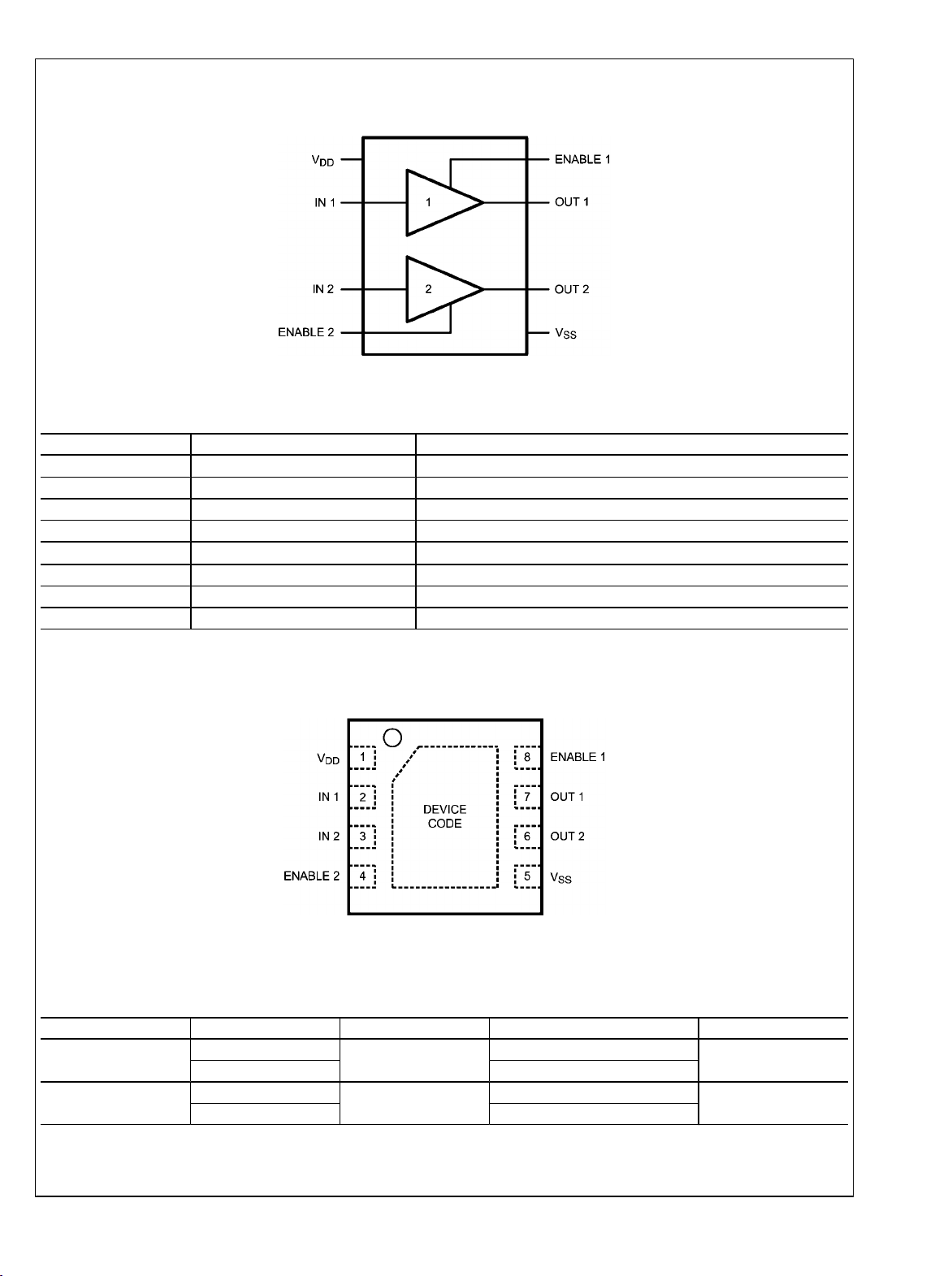
Block Diagram
30024601
Pin Descriptions
Pin No. Pin Name Description
1 V
2 IN 1 Input 1
3 IN 2 Input 2
4 ENABLE 2 Enable buffer 2
5 V
6 OUT 2 Output 2
7 OUT 1 Output 1
8 ENABLE 1 Enable buffer 1
DD
SS
Voltage supply connection
Ground connection
LMH2180
Connection Diagram
8-Pin LLP
Top View
30024631
Ordering Information
Package Part Number Package Marking Transport Media NSC Drawing
8-Pin LLP
Solder Bump
8-Pin LLP
No Pullback
LMH2180YD
LMH2180YDX 4.5k Units Tape and Reel
LMH2180SD
LMH2180SDX 4.5 Units Tape and Reel
LMH2180YD
LMH2180SD
1k Units Tape and Reel
1k Units Tape and Reel
YDA08A
SDA08A
5 www.national.com
 Loading...