

National Semiconductor LMH0346 Technical data
August 19, 2008
LMH0346
3 Gbps HD/SD SDI Reclocker with Dual Differential Outputs
LMH0346 3 Gbps HD/SD SDI Reclocker with Dual Differential Outputs
General Description
The LMH0346 3 Gbps HD/SD SDI Reclocker retimes serial
digital video data conforming to the SMPTE 424M, SMPTE
292M, and SMPTE 259M (C) standards. The LMH0346 operates at serial data rates of 270 Mbps, 1.483 Gbps, 1.485
Gbps, 2.967 Gbps, and 2.97 Gbps. The LMH0346 supports
DVB-ASI operation at 270 Mbps.
The LMH0346 automatically detects the incoming data rate
and adjusts itself to retime the incoming data to suppress accumulated jitter. The LMH0346 recovers the serial data-rate
clock and optionally provides it as an output. The LMH0346
has two differential serial data outputs; the second output may
be selected as a low-jitter, data-rate clock output. Controls
and indicators are: serial clock or second serial data output
select, manual rate select input, SD/HD rate indicator output,
lock detect output, auto/manual data bypass and output mute.
The serial data inputs, outputs, and serial clock outputs are
differential LVPECL compatible. The CML serial data and serial clock outputs are suitable for driving 100Ω differentially
terminated networks. The control logic inputs and outputs are
LVCMOS compatible.
The LMH0346 is powered from a single 3.3V supply. Power
dissipation is typically 370 mW.
The device is available in two space–saving packages: a 6.5
X 4.4 mm 20-pin e-TSSOP and an even more space–efficient
5 X 4 mm 24-pin LLP package.
Features
Supports SMPTE 424M, SMPTE 292M, and SMPTE
■
259M (C) serial digital video standards
Supports 270 Mbps, 1.483 Gbps, 1.485 Gbps, 2.967
■
Gbps, and 2.97 Gbps serial data rate operation
Supports DVB-ASI at 270 Mbps
■
Single 3.3V supply operation
■
370 mW typical power consumption
■
Two differential, reclocked outputs
■
Choice of second reclocked output or low-jitter,
■
differential, data-rate clock output
Single 27 MHz external crystal or reference clock input
■
Manual or automatic rate select input
■
SD/HD operating rate indicator output
■
Lock Detect indicator output
■
Output mute function for data and clock
■
Auto/Manual reclocker bypass
■
Differential LVPECL compatible serial data inputs and
■
outputs
LVCMOS control inputs and indicator outputs
■
20-pin e-TSSOP or 24-pin LLP package
■
Industrial temperature range: -40°C to +85°C
■
Footprint compatible with the LMH0046
■
andLMH0026 (e-TSSOP package)
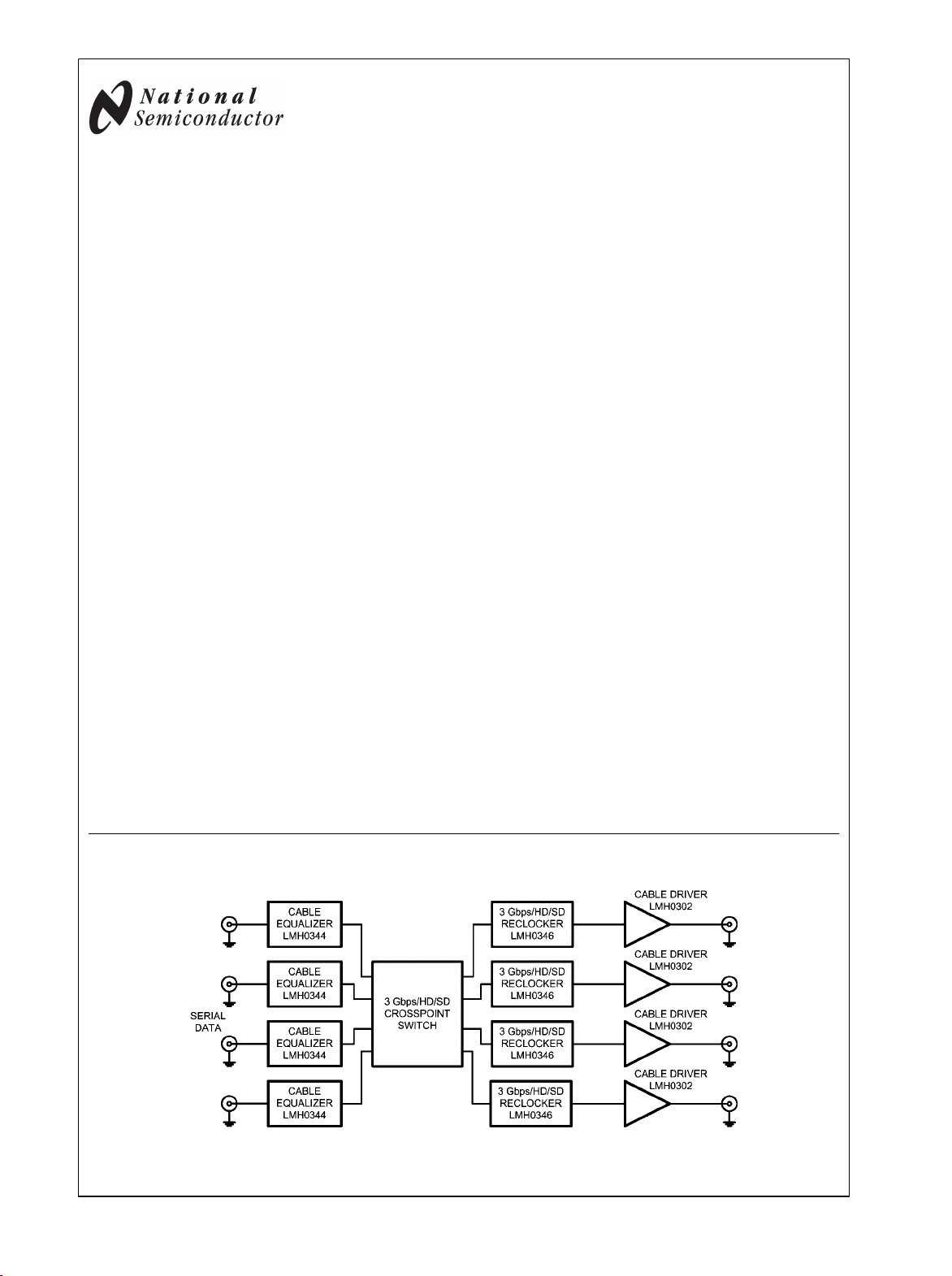
Typical Application
Applications
SDTV/HDTV and 3 Gbps serial digital video interfaces for:
■
Digital video routers and switchers
—
Digital video processing and editing equipment
—
DVB-ASI equipment
—
Video standards and format converters
—
20215001
© 2008 National Semiconductor Corporation 202150 www.national.com
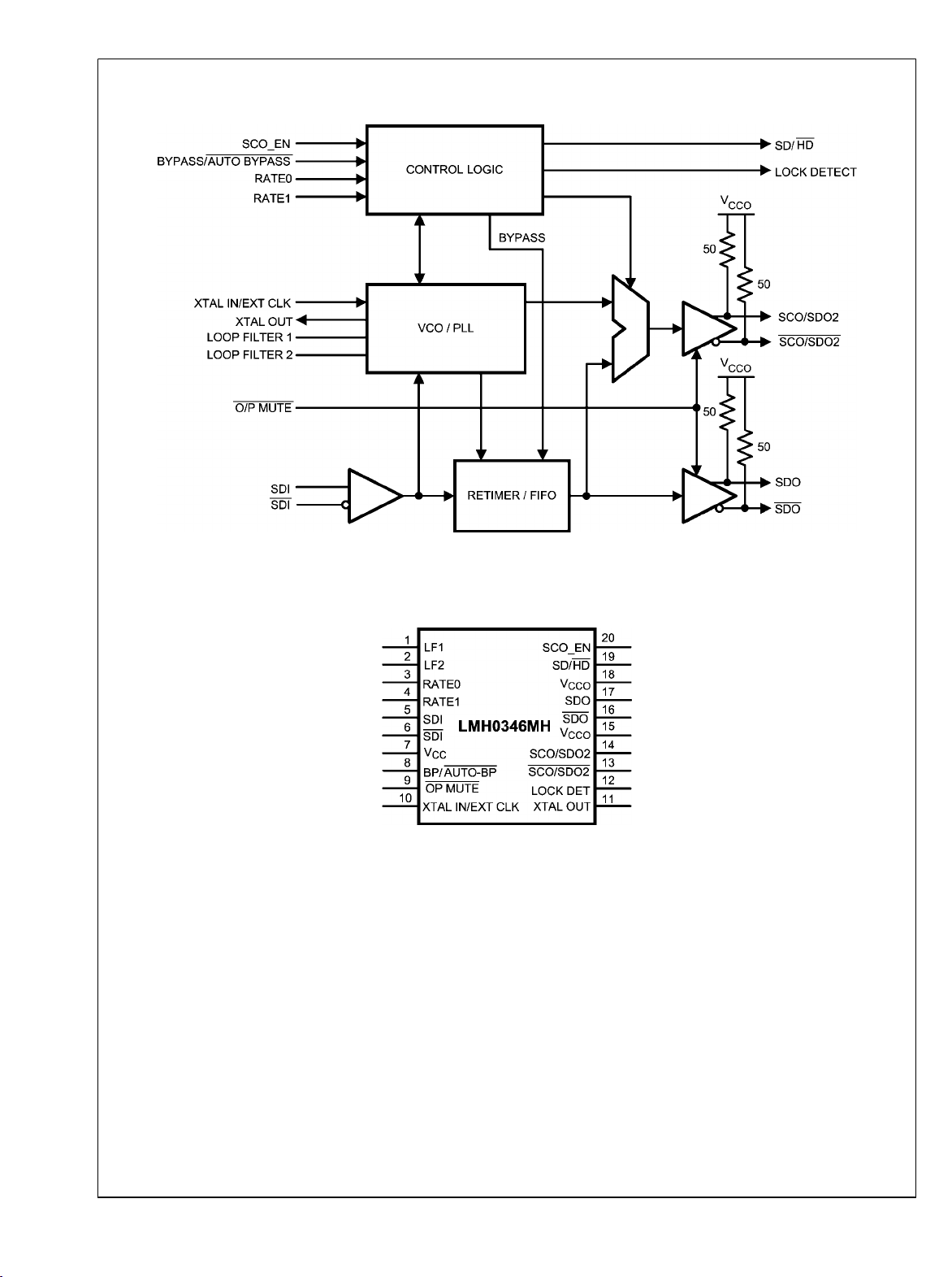
Block Diagram
LMH0346
20215003
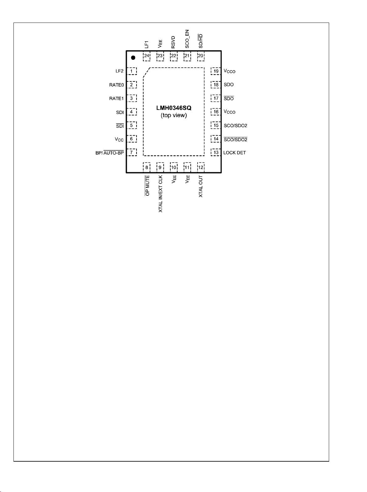
Connection Diagrams
The exposed die attach pad is the negative electrical terminal for this device. It must be connected to the negative power supply voltage.
20-Pin e-TSSOP
Order Number LMH0346MH
See NS Package Number MXA20A
20215002
www.national.com 2
LMH0346
The exposed die attach pad is the primary negative electrical terminal for this device. It must be connected to the negative power supply voltage.
20215006
24-Pin LLP
Order Number LMH0346SQ
See NS Package Number SQA24B
3 www.national.com
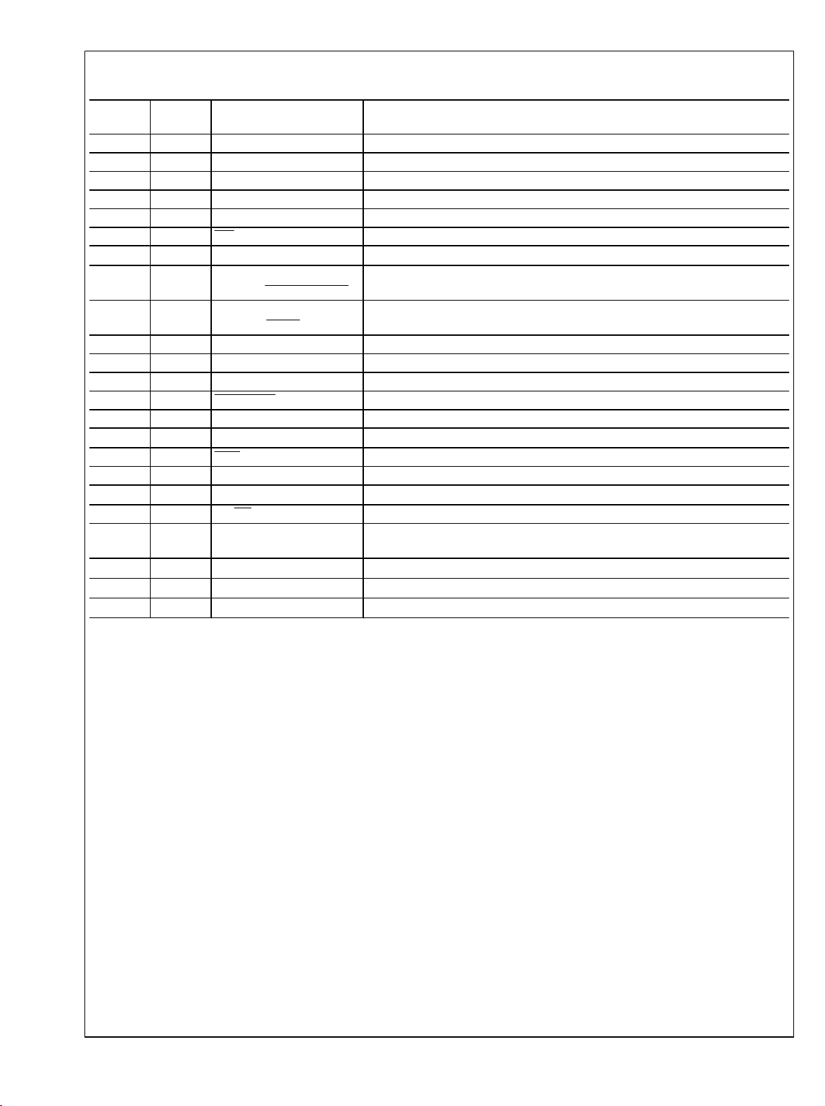
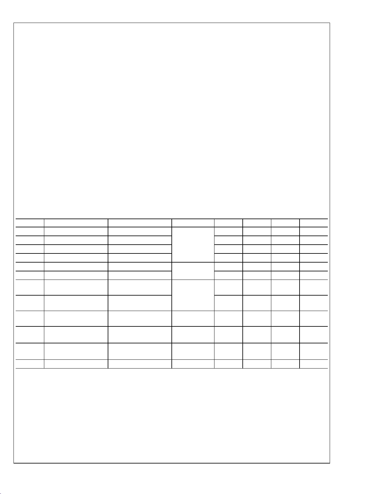
Pin Descriptions
e-TSSOP
LMH0346
Pin
LLP
Pin
Name Description
1 24 LF1 Loop Filter.
2 1 LF2 Loop Filter.
3 2 RATE 0 Data Rate select input. This pin has an internal pulldown
4 3 RATE 1 Data Rate select input. This pin has an internal pulldown
5 4 SDI Data Input True.
6 5 SDI Data Input Complement.
7 6
V
CC
Positive power supply.
Bypass/Auto Bypass mode select. Bypasses reclocking when high. This pin has
8 7 BYPASS/AUTO BYPASS
an internal pulldown.
Data and Clock Output Mute Input. Mutes the output when low. This pin has an
9 8 OUTPUT MUTE
internal pullup.
10 9 XTAL IN/EXT CLK Crystal or External Oscillator Input.
11 12 XTAL OUT Crystal Oscillator Output.
12 13 LOCK DETECT PLL Lock Detect Output (active high).
13 14 SCO/SDO2 Serial Clock or Serial Data Output 2 Complement.
14 15 SCO/SDO2 Serial Clock or Serial Data Output 2 True.
15 16
V
CCO
Positive power supply (Output Driver).
16 17 SDO Data Output Complement.
17 18 SDO Data Output True.
18 19
V
CCO
Positive power supply (Output Driver).
19 20 SD/HD Data Rate Range Output. Output is high for SD and low for HD or 3G.
Serial Clock or Serial Data 2 Output select. Sets second output to output the clock
20 21 SCO_EN
— 10, 11, 23
V
EE
when high and the data when low. This pin has an internal pulldown.
Negative power supply.
— 22 RSVD Reserved for future use. Do not connect.
DAP DAP
V
EE
Connect exposed DAP to negative power supply (ground).
www.national.com 4
LMH0346
Absolute Maximum Ratings (Note 1)
It is anticipated that this device will not be offered in a
military qualified version. If Military/Aerospace specified
devices are required, please contact the National Semiconductor Sales Office/Distributors for availability and specifications.
Supply Voltage (VCC–VEE)
Logic Input Voltage (Vi) VEE−0.15V to V
Logic Input Current (single input):
Vi = VEE−0.15V
Vi = VCC+0.15V
Logic Output Voltage (Vo) VEE−0.15V to V
Logic Output Source/Sink Current ±8 mA
Serial Data Input Voltage (V
Serial Data Output Sink Current (I
) VCC to VCC−2.0V
SDI
)
SDO
4.0V
CC
+0.15V
−5 mA
+5 mA
CC
+0.15V
24 mA
Storage Temp. Range −65°C to +150°C
Junction Temperature +125°C
Lead Temperature (Soldering 4 Sec) +260°C (Pb-free)
ESD Rating (HBM) 8 kV
ESD Rating (MM) 400V
ESD Rating (CDM) 2 kV
Recommended Operating Conditions
Supply Voltage (VCC–VEE)
Logic Input Voltage VEE to V
Differential Serial Input Voltage 800 mV ±10%
Serial Data or Clock Output Sink
Current (ISO)
Operating Free Air Temperature (TA)
3.3V ±5%
16 mA max.
−40°C to +85°C
Package Thermal Resistance
θJA 20-pin e-TSSOP
θJA 24-pin LLP
θJC 20-pin e-TSSOP
θJC 24-pin LLP
26.6°C/W
33.0°C/W
2.4°C/W
3.2°C/W
DC Electrical Characteristics
Over Supply Voltage and Operating Temperature ranges, unless otherwise specified. (Notes 2, 3)
Symbol Parameter Conditions Reference Min Typ Max Units
V
V
V
V
V
V
V
V
V
SDOD
SCOD
I
Input Voltage High Level Logic inputs
IH
Input Voltage Low Level V
IL
I
Input Current High Level VIH = V
IH
I
Input Current Low Level VIL = V
IL
Output Voltage High Level IOH = −2 mA Logic outputs
OH
Output Voltage Low Level IOL = +2 mA
OL
Serial Input Voltage,
SDID
CC
EE
(Note 8) SDI
Differential
Input Common Mode
CMI
V
= 200 mV, (Note 8)
SDID
Voltage
Serial Data Output
100Ω differential load
SDO
Voltage, Differential
Serial Clock Output
Voltage, Differential
Output Common Mode
CMO
100Ω differential load,
2970 Mbps, (Note 8)
100Ω differential load
SCO
SDO, SCO
Voltage
Supply Current 2970 Mbps
CC
2
EE
0.8 V
V
CC
47 65 µA
−18 −25 µA
2 V
VEE + 0.6
200 1600
VEE+1.2
VCC−0.2
620 750 880
400 525 650
VCC−
V
SDOD
V
111 126 mA
mV
mV
mV
V
V
P-P
V
P-P
P-P
CC
5 www.national.com
 Loading...