

National Semiconductor LMH0340, LMH0341 User Manual
User Guide: SDALTEVK HSMC SDI ADAPTER BOARD
9-Jul-09 Version 0.06
SDI Development Kit using National
Semiconductor’s LMH0340
serializer and LMH0341 deserializer
July 2009 Rev 0.06
Page 1 of 31

....Overview 3
1
2....Evaluation Kit (SDALTEVK) Contents 3
3....Hardware Setup 5
3.1 CYCLONE III DEVELOPMENT BOARD (MAIN BOARD) DESCRIPTION.................................................................... 6
3.2 SDALTEVK BOARD DESCRIPTION................................................................................................................. 8
4....Software Setup 9
4.1 INSTALLATION................................................................................................................................................ 9
4.2 STARTUP .................................................................................................................................................... 10
5....Evaluating Hardware 13
5.1 TEST SETUPS.............................................................................................................................................. 13
5.1.1 Standalone Video Generator Tests ...................................................................................................13
5.1.2 Genlock Tests.................................................................................................................................... 14
5.1.3 Video Pass-through Tests ................................................................................................................. 15
5.2 TERMINAL BASED SD/HD/3G SDI EVALUATION............................................................................................ 15
5.2.1 Standalone Mode............................................................................................................................... 16
5.2.2 Pass-through Mode ........................................................................................................................... 17
5.2.3 Genlocked Mode..................................................................................Error! Bookmark not defined.
5.3 PUSH BUTTON BASED SD/HD/3G SDI EVALUATION ..................................................................................... 19
5.3.1 Push Button Main Menu .................................................................................................................... 19
5.3.2 System Mode..................................................................................................................................... 20
5.3.3 Datapath Menu .................................................................................................................................. 20
5.3.4 Video Format Menu ........................................................................................................................... 20
5.3.5 Frequency Menu................................................................................................................................ 21
5.4 FPGA REGISTER MAP................................................................................................................................. 21
5.4.1 Miscellaneous Registers:................................................................................................................... 22
5.4.2 Reset Registers ................................................................................................................................. 22
5.4.3 Rx Video Registers............................................................................................................................ 22
5.4.4 Datapath Registers............................................................................................................................ 24
5.4.5 Clocking ............................................................................................................................................. 26
5.4.6 Video Timing...................................................................................................................................... 26
5.5 SUPPORTED TEST PATTERNS....................................................................................................................... 29
6....Documentation 30
7....Schematics, BOMs, and Data Sheets 30
8....Reference FPGA IP 30
9....Up to Date Information 30
10 ..Part Numbers 30
July 2009 Rev 0.06
Page 2 of 31
1 Overview
The SDALTEVK enables rapid evaluation of the LMH0340/0341 serializer and deserializer in Serial Digital
Interface (SDI) applications. Other National devices also highlighted on this board are shown in Table 1.
Table 1) National Semiconductor Devices on the SDALTEVK
Device Quantity Description Function Reference
Designator
LMH0340 2 SD, HD and 3G SDI serializer +
cable driver
LMH0341 1 SD, HD and 3G SDI deserializer SDI Deserializer U11
LMH0344 1 SD, HD and 3G cable equalizer SDI Equalizer U13
LMH1981 1 Multi-Format Video Sync
Separator
LMH1982 1 Multi-Rate Video Clock
Generator with Genlock
DS90CP22 1 2x2 LVDS Cross Point Switch Clock Multiplexer U7
DS90LV028
A
DS90LV031
A
LP3878-ADJ 1 Micropower 800mA Low Noise
LM20242 1 2A PowerWise™ Adjustable
Examples of firmware are provided for the Standard Definition SMPTE 259M (SD-SDI) interface, the High
Definition SMPTE 292M (HD-SDI) interface, and the 3G SMPTE 424M (3G-SDI) interface. The video standards
supported by the example firmware are shown in Table 2.
Rate Video Standard
SD NTSC, PAL
HD 720p50, 720p59, 720p60, 1080s23.98, 1080s24, 1080i50, 1080i59, 1080i60,
1080p29.97, 1080p30
3G 1080p50, 1080p59.9, 1080p60
A user interface allows for managing the FPGA firmware functions and the LMH0340/0341/1982 device registers.
1 Dual LVDS to 3V CMOS
Receiver
1 Quad 3V CMOS to LVDS Line
Driver
Adjustable Voltage Regulator
Frequency Synchronous Buck
Regulator
Table 2) Video Standards Supported by Firmware
SDI Serializer U1, U6
Optional Clock
Source
Optional Clock
Source
Optional Clock
Output
Optional Clock
Source
2.5V Regulator U10
3.3V Regulator U12
U3
U9
U5
U2
2 Evaluation Kit (SDALTEVK) Contents
The SDALTEVK contains the following parts:
SDALTEVK HSMC SDI ADAPTER Board
Screws, standoffs and spacers for mounting the EVK to the Cyclone III Development Board
July 2009 Rev 0.06
Page 3 of 31

The following is required to complete the evaluation kit:
Altera Cyclone III Development Kit Altera Part Number: DK-DEV-3C120N
National Semiconductor SDI compiled .sof file from: http://www.national.com/sdaltevk
o Triple Rate Standalone mode with multiple format selection
o Triple Rate pass-thru mode with format detection
o Pattern selection
o Gen-Lock function supported
o Register programming supported
Altera compiled .sof file from: ftp://ftp.altera.com/outgoing/National_SerDes/an535_1_0.zip
o Triple Rate pass-thru mode
Quartus II 8.0 or newer http://www.altera.com/products/
Nios II EDS 8.0 http://www.altera.com/products/
Cygwin from http://www.cygwin.com/
SDI cables
PC
July 2009 Rev 0.06
Page 4 of 31
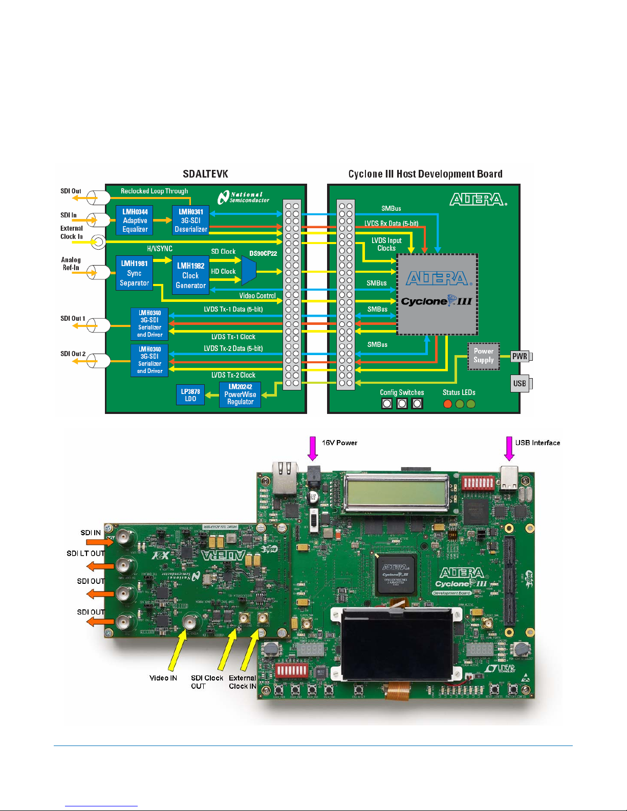
Hardware Setup
The SDALTEVK printed circuit board is designed to interface with the HSMC connector on the Cyclone III
Development Boards. Power, control bus, and LVDS bus signals are supplied to the daughter board through the
HSMC connector. The Cyclone III FPGA provides the SD/HD/3G SDI and general purpose stacks as well as the
control interface to a PC through a USB cable. This evaluation system allows inexpensive FPGAs to deliver up to
3 Gbps on a coax cable.
Figure 1 Evaluation Kit Block Diagram
July 2009 Rev 0.06
Figure 2 Evaluation Kit Connections
Page 5 of 31
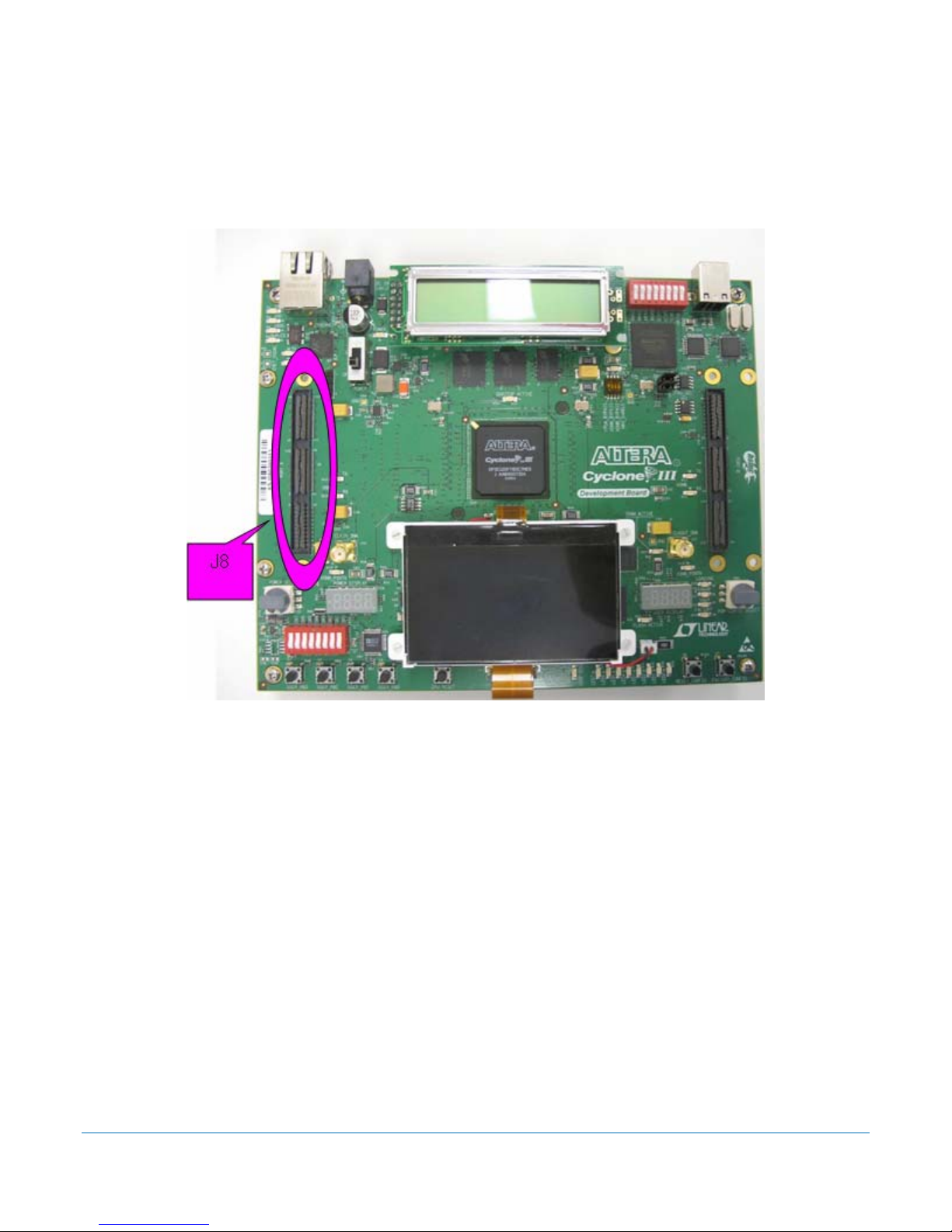
2.1 Cyclone III Development Board (Main Board) Description
The main board has a Cyclone III FPGA. The FPGA provides the SD/HD/3G SDI and general purpose stacks as
well as the control interfaces through the supplied example firmware. The daughter board is connected to the
main board through the high speed mezzanine connector (HSMC), J8. This connector provides power, control
bus, and data bus. The main board communicates to a PC through a USB cable.
Figure 3 Cyclone III Development Board
2.2 Cyclone III Development Board Termination Resistors
The Altera Cyclone III device does not have any internal termination on the receive LVDS I/O’s. Termination
resistors must be added to the Cyclone III board. The terminations resistors must be placed as close to the
FPGA’s pin as possible. The 3C120 host board has the layout footprints for the termination resistors. Eleven 100
Ohm resistors in 0402 package size are required to install onto the host board. The resistors are located on the
bottom side of the board. They are between the FPGA and the HSMC port A connector. Figures 4 and 5 show the
schematic and board location of the LVDS termination resistors.
July 2009 Rev 0.06
Page 6 of 31
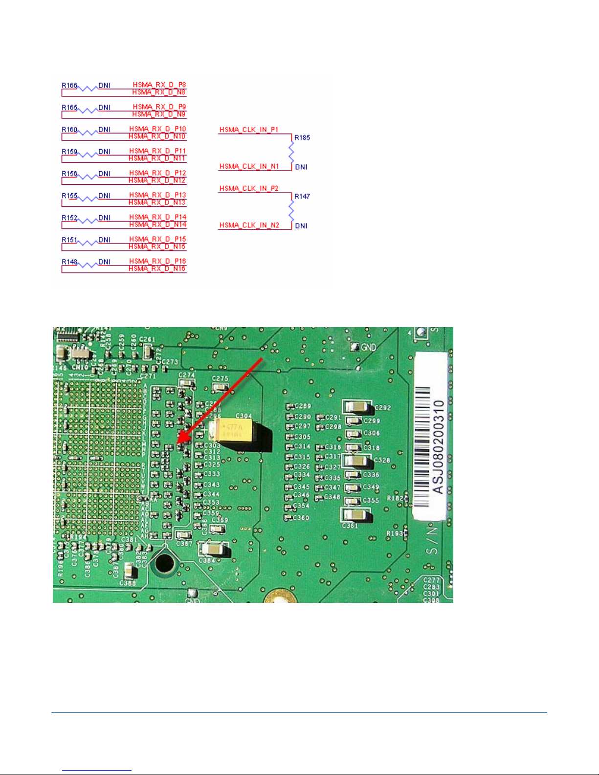
Figure 4 Resistors on HSCM port A
Figure 5 Photograph of the back of the Cyclone III board showing location of the 100 Ohm Resistors
July 2009 Rev 0.06
Page 7 of 31
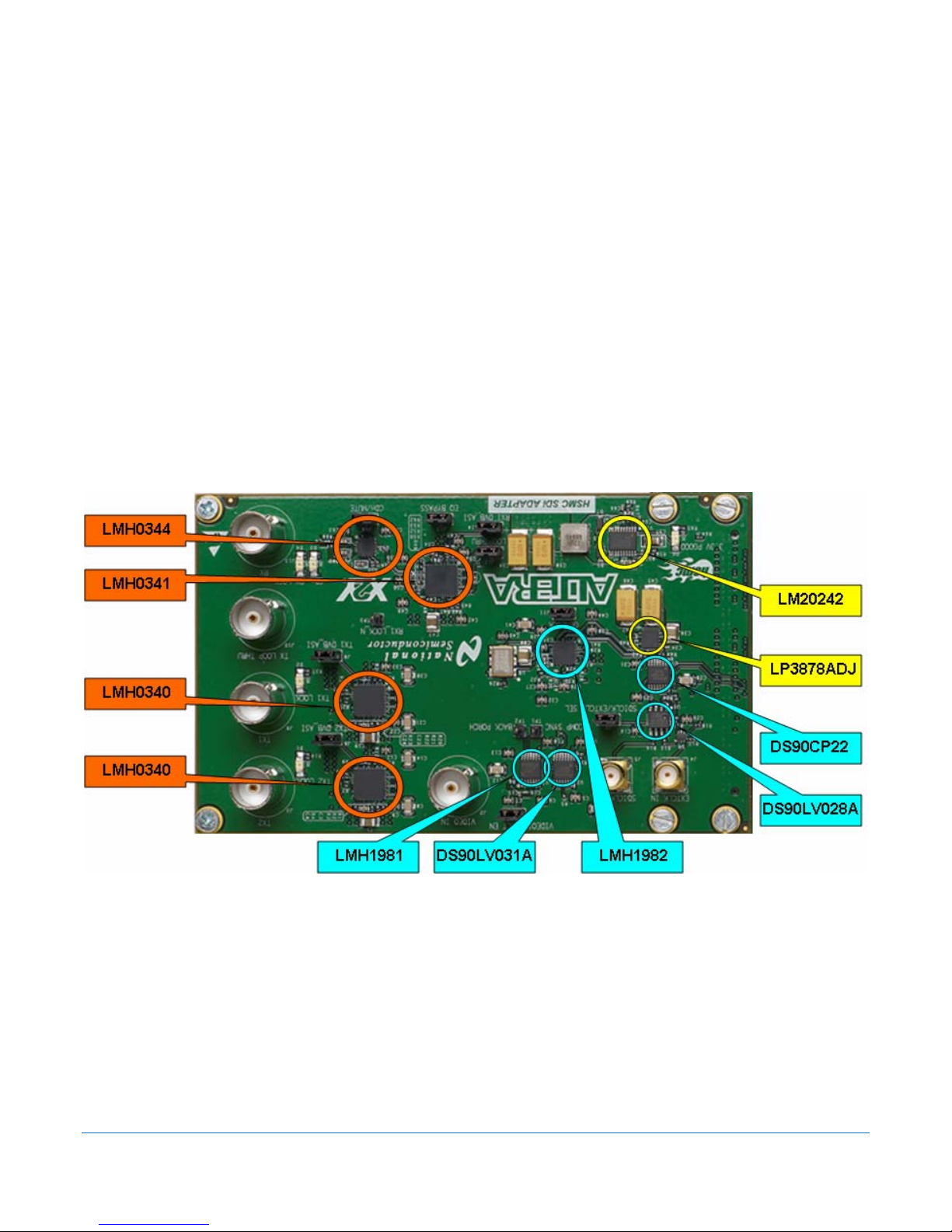
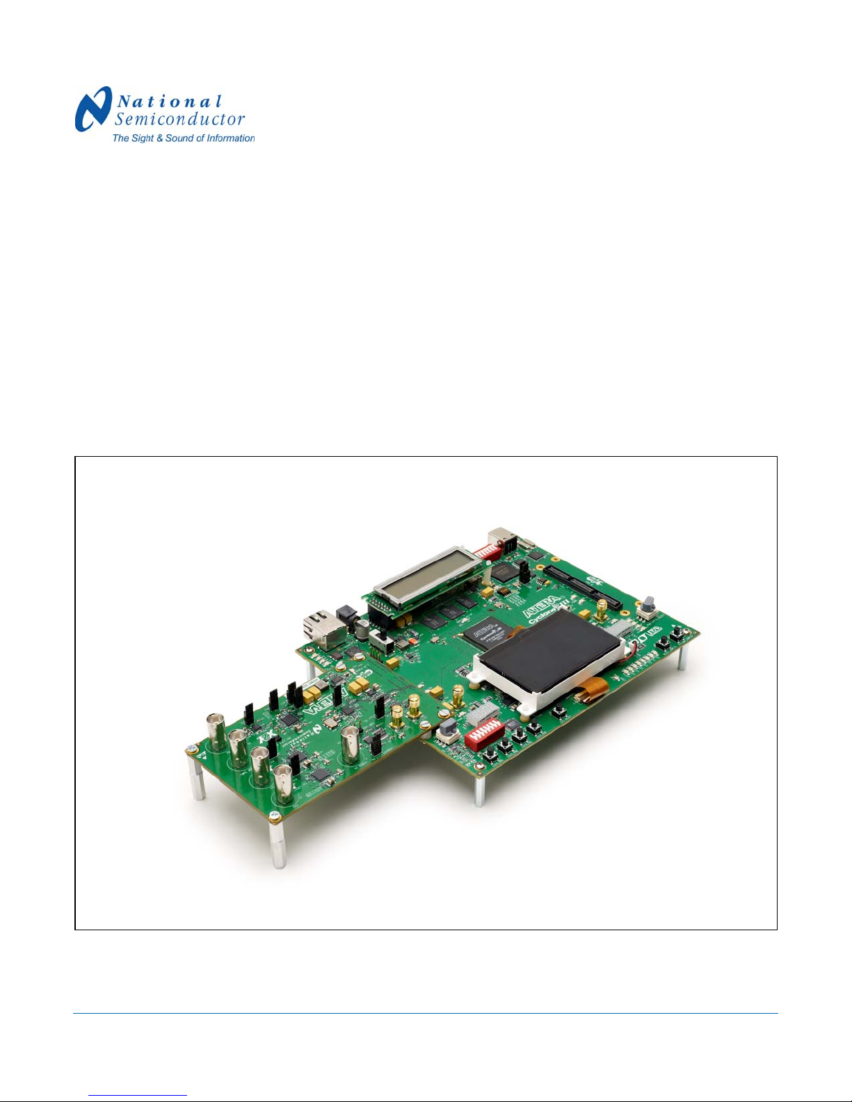
2.3 SDALTEVK Board Description
The HSMC SDI ADAPTER board features the 5:1 LMH0340 serializer IC with integrated cable driver, the 1:5
LMH0341 deserializer IC and the LMH0344 adaptive cable equalizer IC, all highlighted in orange. These devices
support SD, HD, or 3G SDI interfaces across 75 ohm coaxial cable, which can interface with the board via BNC
connectors J3, J8, J10, or J13.
For added testing flexibility, the additional components shown in blue allow for several different clocking schemes.
All of the clocking schemes are controlled by the DS90CP22 which is used to multiplex the various clock sources
to the FPGA. The LMH1981 receives analog video via BNC connector J2 and provides the HSYNC and VSYNC
to the LMH1982 for clock generation. The LMH1982 can also generate a clock based on a local 27 MHz
oscillator. By using the DS90LV031A, an external clock can be applied to the card at SMA connector J4. In order
to observe the quality of the clock provided to the FPGA, the clock can be routed to the DS90LV028A which will
drive a CMOS clock out of SMA connector J5.
Power is provided to the board via two separate power rails that travel across the HSMC connector from the
Cyclone III host board. The Powerwise® LM20242 adjustable frequency synchronous buck regulator supplies the
3.3V power for the evaluation card by using the 12V rail from the host board. The LP3878ADJ low noise regulator
uses the 3V power of the host board to supply the 2.5V power to the evaluation card.
July 2009 Rev 0.06
Figure 6 SDALTEVK
Page 8 of 31

3 Software Setup
3.1 Installation
Make sure the Altera hardware is not connected to the PC. The following installation instructions are for the
Windows XP Operating System. Quartus II 8.0 or newer is required to properly operate the SDALTEVK. If the
terminal interface is desired then Nios II EDS 8.0 or newer must also be installed on the PC. If an older version of
either Quartus II or Nios II EDS is already installed, make sure that it is updated before attempting to use the
SDALTEVK. If necessary, please see http://www.altera.com/products/
In order to use the Nios II terminal interface, Cygwin must be installed on the PC. Visit http://www.cygwin.com/
download the latest version of Cygwin for free. Make sure that the file “cygwin1.dll” is installed to the path:
C:\altera\80\nios2eds\bin
Install the Quartus II 8.0 Software
Execute the Quartus II 8.0 software installation program. The program is called “80_quartus_windows.exe”. This
will load the driver files onto the PC.
Follow the install instructions prompted by the Quartus install daemon
Install the Nios II EDS 8.0 Software
Execute the Nios II EDS installation program. The program is called “80_nios2eds_windows.exe”.
Follow the install instructions prompted by the Nios II install daemon
The software installation is complete.
to download the latest software.
to
July 2009 Rev 0.06
Page 9 of 31
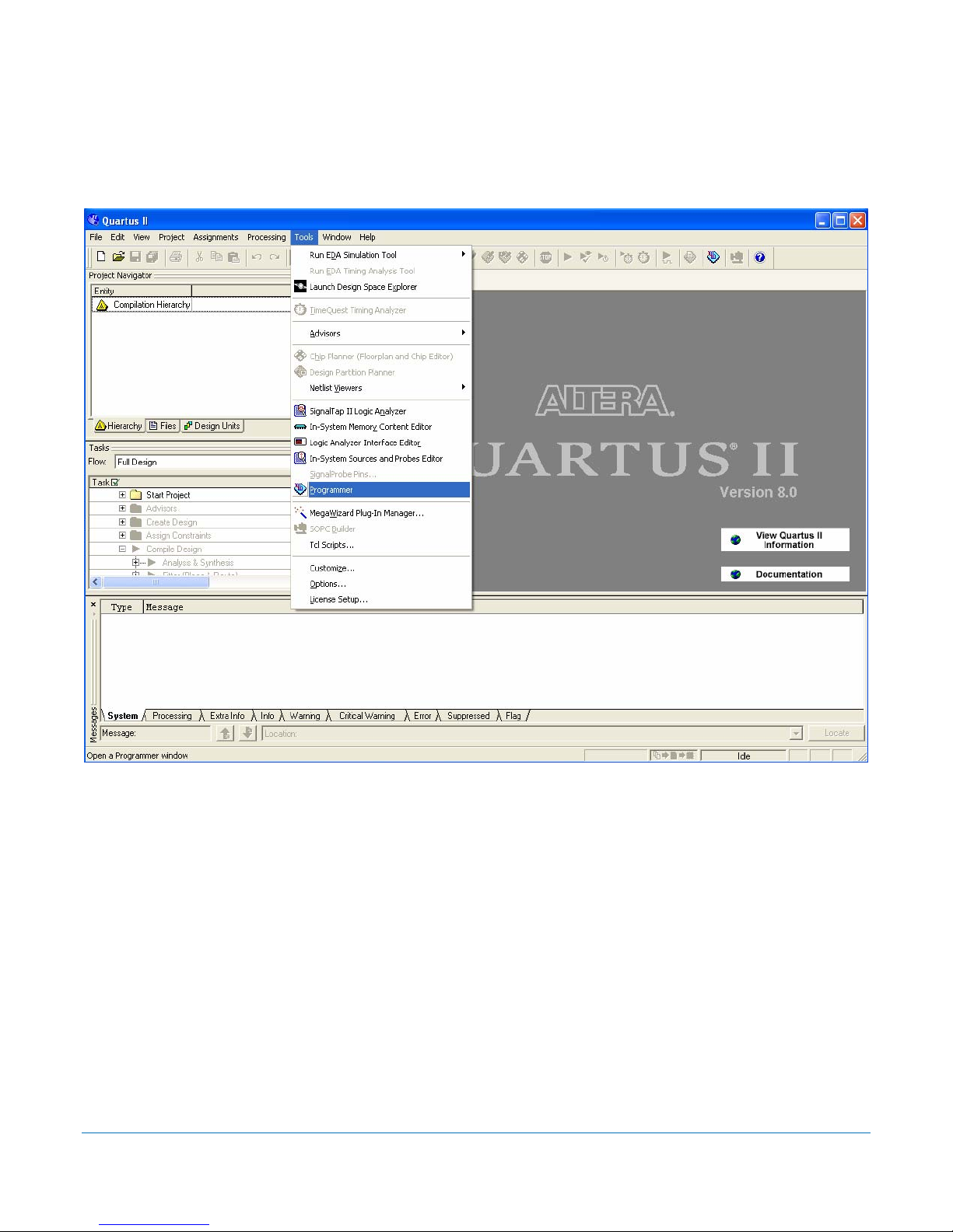
3.2 Startup
Make sure all the software has been installed and the hardware is powered on and connected to the PC. Run
Quartus II by either by using the path “C:\altera\80\quartus\bin\quartus.exe” or selecting it from the “altera” folder
in the start menu. Once the software has loaded go to the “Tools” menu, and select “Programmer.”
Figure 7 Quartus Main Screen
July 2009 Rev 0.06
Page 10 of 31
 Loading...