

www.DataSheet4U.com
查询LMH0034供应商查询LMH0034供应商
LMH0034
SMPTE 292M / 259M Adaptive Cable Equalizer
LMH0034 SMPTE 292M / 259M Adaptive Cable Equalizer
PRELIMINARY
January 2006
General Description
The LMH0034 SMPTE 292M / 259M adaptive cable equalizer is a monolithic integrated circuit for equalizing data
transmitted over cable (or any media with similar dispersive
loss characteristics). The equalizer operates over a wide
range of data rates from 143 Mbps to 1.485 Gbps and
supports SMPTE 292M, SMPTE 344M and SMPTE 259M.
The LMH0034 implements DC restoration to correctly handle
pathological data conditions. DC restoration can be bypassed for low data rate applications. The equalizer is flexible in allowing either single-ended or differential input drive.
Additional features include a combined carrier detect and
output mute pin which mutes the output when no signal is
present. A programmable mute reference is used to mute the
output at a selectable level of signal degradation. A cable
length indicator is provided to determine the amount of cable
being equalized.
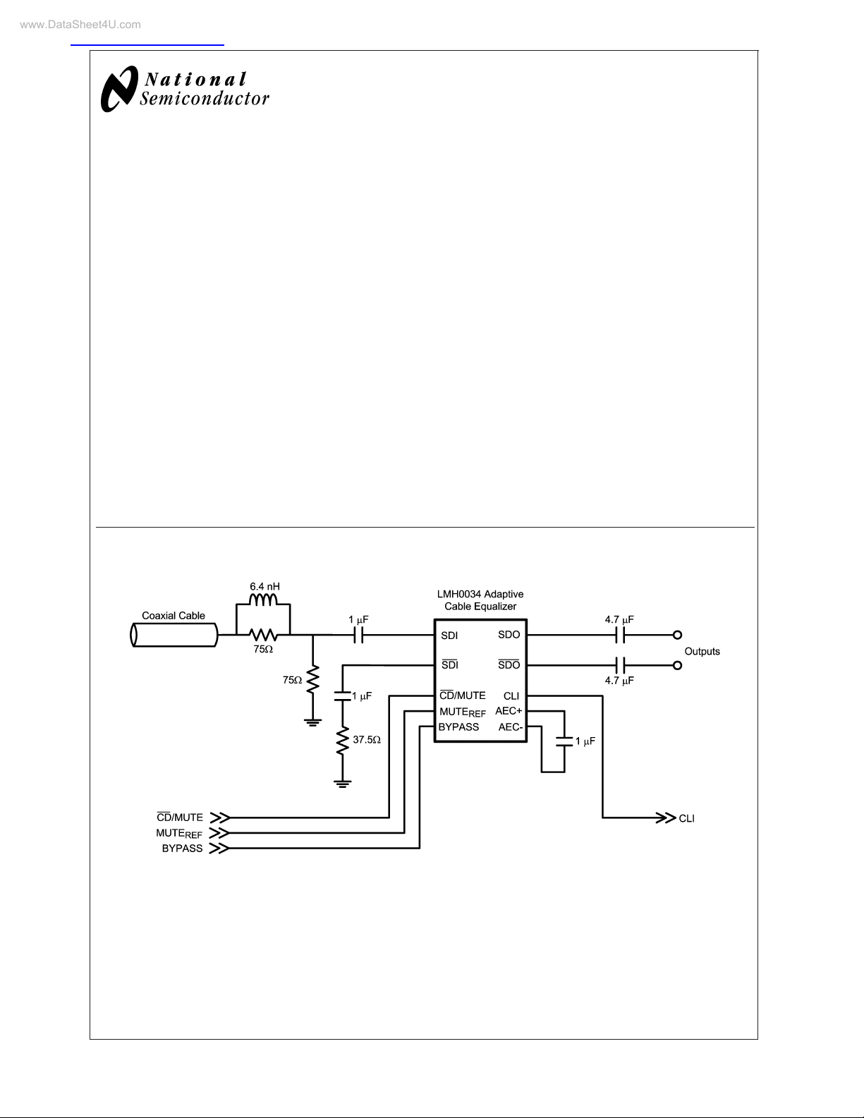
Typical Application
Features
n SMPTE 292M, SMPTE 344M and SMPTE 259M
compliant
n Supports DVB-ASI at 270 Mbps
n High data rates: 143 Mbps to 1.485 Gbps
n Equalizes up to 140 meters of Belden 1694A at 1.485
Gbps or up to 350 meters of Belden 1694A at 270 Mbps
n Manual bypass, cable length indicator, and output mute
with a programmable threshold
n Single-ended or differential input
n 50Ω differential outputs
n Single 3.3V supply operation
n 208mW typical power consumption with 3.3V supply
n Replaces the GS1524 and GS1524A
Applications
n SMPTE 292M, SMPTE 344M, and SMPTE 259M serial
digital interfaces
n Serial digital data equalization and reception
n Data recovery equalization
© 2006 National Semiconductor Corporation DS201734 www.national.com
20173401
Absolute Maximum Ratings (Note 1)
Supply Voltage −0.5V to 3.6V
LMH0034
Input Voltage (all inputs) −0.3V to V
Storage Temperature Range −65˚C to +150˚C
Junction Temperature +150˚C
Lead Temperature
(Soldering 4 Sec) +260˚C
CC
+0.3V
Recommended Operating
Conditions
Supply Voltage (VCC–VEE) 3.3V±5%
Input Coupling Capacitance 1.0 µF
AEC Capacitor (Connected between
AEC+ and AEC-) 1.0 µF
Operating Free Air Temperature (T
) 0˚C to +85˚C
A
Package Thermal Resistance
θ
16-pin SOIC
JA
16-pin SOIC
θ
JC
+115˚C/W
+105˚C/W
ESD Rating (HBM) 8kV
ESD Rating (MM) 250V
DC Electrical Characteristics
Over Supply Voltage and Operating Temperature ranges, unless otherwise specified (Notes 2, 3).
Symbol Parameter Conditions Reference Min Typ Max Units
V
CMIN
V
SDI
V
CMOUT
V
SDO
I
CC
Input Common Mode Voltage SDI, SDI 1.9 V
Input Voltage Swing At LMH0034 input, (Notes 4, 6) 720 800 950 mV
Output Common Mode Voltage SDO, SDO VCC–
/2
V
SDO
Output Voltage Swing 50Ω load, differential 750 mV
CLI DC Voltage 0m cable CLI 2.5 V
Max cable 1.6 V
MUTE
MUTE
CD/MUTE Output Voltage
DC Voltage (floating) MUTE
REF
Range 0.7 V
REF
REF
1.3 V
Carrier not present CD/MUTE 2.6 V
Carrier present 0.4 V
CD/MUTE Input Voltage
Min to mute outputs 3.0 V
Max to force outputs active 2.0 V
Supply Current (Note 7) 63 77 mA
P−P
V
P-P
www.national.com 2

AC Electrical Characteristics
Over Supply Voltage and Operating Temperature ranges, unless otherwise specified (Note 3).
Symbol Parameter Conditions Reference Min Typ Max Units
BR
t
r,tf
t
OS
R
RL
R
C
OUT
IN
IN
Input Data Rate SDI, SDI 143 1485 Mbps
SDI
Maximum Equalized Cable
Length (with equalizer
pathological)
270 Mbps, Belden 1694A,
0.2UI output jitter, (Note 4)
270 Mbps, Belden 8281,
0.2UI output jitter, (Note 4)
1.485 Gbps, Belden 1694A,
0.25UI output jitter, (Note 4)
1.485 Gbps, Belden 8281,
0.25UI output jitter, (Note 4)
350 m
280 m
140 m
100 m
Output Rise Time, Fall Time 20% – 80%, (Note 4) SDO, SDO 100 220 ps
Mismatch in Rise/Fall Time (Note 4) 2 15 ps
Output Overshoot (Note 4) 1 5 %
Output Resistance single-ended, (Note 5) 50 Ω
Input Return Loss (Note 8) SDI, SDI 15 18-20 dB
IN
Input Resistance single-ended 1.3 kΩ
Input Capacitance single-ended, (Note 5) 1 pF
Note 1: "Absolute Maximum Ratings" are those parameter values beyond which the life and operation of the device cannot be guaranteed. The stating herein of
these maximums shall not be construed to imply that the device can or should be operated at or beyond these values. The table of "Electrical Characteristics"
specifies acceptable device operating conditions.
Note 2: Current flow into device pins is defined as positive. Current flow out of device pins is defined as negative.All voltages are stated referenced to V
Note 3: Typical values are stated for V
Note 4: Specification is guaranteed by characterization.
Note 5: Specification is guaranteed by design.
Note 6: The maximum input voltage swing assumes a nonstressing, DC-balance signal; specifically, the SMPTE-recommended color bar test signal. Pathological
or other stressing signals may not be used. This specification is for 0m cable only.
Note 7: Supply current depends on the amount of cable being equalized. The current is highest for short cable and decreases as the cable length is increased. Refer
to Figures 1, 2.
Note 8: Input return loss is dependent on board design. The LMH0034 meets this specification on the SD034 evaluation board from 5MHz to 1.5GHz.
= +3.3V and TA= +25˚C.
CC
= 0 Volts.
EE
LMH0034
www.national.com3

Connection Diagram
LMH0034
16-Pin SOIC
20173403
Order Number LMH0034MA
See NS Package Number M16A
Pin Descriptions
Pin # Name Description
1 CLI Cable length indicator. Provides a voltage inversely proportional to the cable length being
equalized.
2V
3V
CC
EE
4 SDI Serial data true input.
5 SDI
6V
EE
7 AEC+ AEC loop filter external capacitor (1µF) positive connection.
8 AEC- AEC loop filter external capacitor (1µF) negative connection.
9 BYPASS Bypasses equalization and DC restoration when high. No equalization occurs in this mode.
10 MUTE
11 V
REF
EE
12 SDO
13 SDO Serial data true output.
14 V
15 V
EE
CC
16 CD/MUTE
Positive power supply (+3.3V).
Negative power supply (ground).
Serial data complement input.
Negative power supply (ground).
Mute reference. Determines the maximum cable to be equalized before muting. May be
unconnected for maximum equalization.
Negative power supply (ground).
Serial data complement output.
Negative power supply (ground).
Positive power supply (+3.3V).
Bi-directional carrier detect and output mute. CD/MUTE is high when no signal is present. If
unconnected, MUTE is controlled automatically by carrier detect. To force MUTE on, tie to
. To disable MUTE, tie to GND. CD/MUTE has no function in BYPASS mode.
V
CC
www.national.com 4

Block Diagram
LMH0034
Device Operation
BLOCK DESCRIPTION
The Equalizer Filter block is a multi-stage adaptive filter. If
Bypass is high, the equalizer filter is disabled.
The DC Restoration / Level Control block receives the
differential signals from the equalizer filter block. This block
incorporates a self-biasing DC restoration circuit to fully DC
restore the signals. If Bypass is high, this function is disabled.
The signals before and after the DC Restoration / Level
Control block are used to generate the Automatic Equal-
ization Control (AEC) signal. This control signal sets the
gain and bandwidth of the equalizer filter. The loop response
in the AEC block is controlled by an external 1µF capacitor
placed across the AEC+ and AEC- pins. Cable Length
Indicator (CLI) is derived from this block.
The Carrier Detect / Mute block generates the carrier detect
signal and controls the mute function of the output. This
block utilizes the bi-directional CD/MUTE signal along with
Mute Reference (MUTE
The Output Driver produces SDO and SDO.
CABLE LENGTH INDICATOR (CLI)
The cable length indicator provides a voltage to indicate the
length of cable being equalized. The CLI voltage decreases
as the cable length increases.
MUTE REFERENCE (MUTE
The mute reference determines the amount of cable to
equalize before automatically muting the outputs. This is set
by applying a voltage inversely proportional to the length of
REF
).
REF
)
20173402
cable to equalize. As the applied MUTE
voltage is in-
REF
creased, the amount of cable that can be equalized before
carrier detect is de-asserted and the outputs are muted is
decreased. MUTE
may be left unconnected for maximum
REF
equalization before muting.
CARRIER DETECT / MUTE (CD/MUTE)
Carrier Detect / Mute is bi-directional, serving as both a
carrier detect (output function) and mute (input function).
When used as an output, CD/MUTE determines if a valid
signal is present at the LMH0034 input. If MUTE
REF
is used,
the carrier detect threshold will be altered accordingly.
CD/MUTE provides a high voltage when no signal is present
at the LMH0034 input, and the outputs are automatically
muted. CD/MUTE is low when a valid input signal has been
detected, and the outputs are automatically enabled.
As an input, CD/MUTE can be used to override the carrier
detect and manually mute or enable the LMH0034 outputs.
Applying a high input to CD/MUTE will mute the LMH0034
outputs. Applying a low input will force the outputs to be
active regardless of the length of cable or the state of
REF
.
MUTE
INPUT INTERFACING
The LMH0034 accepts either differential or single-ended
input. The input must be AC coupled. Transformer coupling
is not supported.
The LMH0034 correctly handles equalizer pathological signals for standard definition and high definition serial digital
video, as described in SMPTE RP 178 and RP 198, respectively.
www.national.com5

Device Operation (Continued)
OUTPUT INTERFACING
LMH0034
The SDO and SDO outputs are internally loaded with 50Ω.
They produce a 750 mV
375 mV
single-ended output.
P-P
differential output, or a
P-P
Application Information
PCB LAYOUT RECOMMENDATIONS
Please refer to the following Application Note on National’s
website: AN-1372, “CLC034 PCB Layout Techniques.”
REPLACING THE GENNUM GS1524
The LMH0034 is form-fit-function compatible with the Gennum GS1524 and GS1524A.
SUPPLY CURRENT VS. CABLE LENGTH
The supply current (I
being equalized. The current is highest for short cable and
decreases as the cable length is increased. Figure 1 shows
supply current vs. Belden 1694A cable length for 1.485 Gbps
data and Figure 2 shows supply current vs. Belden 1694A
cable length for 270 Mbps data.
) depends on the amount of cable
CC
20173415
FIGURE 2. Supply Current vs. Belden 1694A Cable
Length, 270 Mbps
20173413
FIGURE 1. Supply Current vs. Belden 1694A Cable
Length, 1.485 Gbps
www.national.com 6

Physical Dimensions inches (millimeters) unless otherwise noted
16-Pin SOIC
Order Number LMH0034MA
NS Package Number M16A
LMH0034 SMPTE 292M / 259M Adaptive Cable Equalizer
National does not assume any responsibility for use of any circuitry described, no circuit patent licenses are implied and National reserves
the right at any time without notice to change said circuitry and specifications.
For the most current product information visit us at www.national.com.
LIFE SUPPORT POLICY
NATIONAL’S PRODUCTS ARE NOT AUTHORIZED FOR USE AS CRITICAL COMPONENTS IN LIFE SUPPORT DEVICES OR SYSTEMS
WITHOUT THE EXPRESS WRITTEN APPROVAL OF THE PRESIDENT AND GENERAL COUNSEL OF NATIONAL SEMICONDUCTOR
CORPORATION. As used herein:
1. Life support devices or systems are devices or systems
which, (a) are intended for surgical implant into the body, or
(b) support or sustain life, and whose failure to perform when
properly used in accordance with instructions for use
2. A critical component is any component of a life support
device or system whose failure to perform can be reasonably
expected to cause the failure of the life support device or
system, or to affect its safety or effectiveness.
provided in the labeling, can be reasonably expected to result
in a significant injury to the user.
BANNED SUBSTANCE COMPLIANCE
National Semiconductor manufactures products and uses packing materials that meet the provisions of the Customer Products
Stewardship Specification (CSP-9-111C2) and the Banned Substances and Materials of Interest Specification (CSP-9-111S2) and contain
no ‘‘Banned Substances’’ as defined in CSP-9-111S2.
Leadfree products are RoHS compliant.
National Semiconductor
Americas Customer
Support Center
Email: new.feedback@nsc.com
Tel: 1-800-272-9959
www.national.com
National Semiconductor
Europe Customer Support Center
Fax: +49 (0) 180-530 85 86
Email: europe.support@nsc.com
Deutsch Tel: +49 (0) 69 9508 6208
English Tel: +44 (0) 870 24 0 2171
Français Tel: +33 (0) 1 41 91 8790
National Semiconductor
Asia Pacific Customer
Support Center
Email: ap.support@nsc.com
National Semiconductor
Japan Customer Support Center
Fax: 81-3-5639-7507
Email: jpn.feedback@nsc.com
Tel: 81-3-5639-7560
 Loading...