

LMH0031
SMPTE 292M/259M Digital Video Deserializer /
Descrambler with Video and Ancillary Data FIFOs
General Description
The LMH0031 SMPTE 292M / 259M Digital Video
Deserializer/Descrambler with Video and Ancillary Data
FIFOs is a monolithic integrated circuit that deserializes and
decodes SMPTE 292M, 1.485Gbps (or 1.483Gbps) serial
component video data, to 20-bit parallel data with a synchronized parallel word-rate clock. It also deserializes and decodes SMPTE 259M, 270Mbps, 360Mbps and
SMPTE 344M (proposed) 540Mbps serial component video
data, to 10-bit parallel data. Functions performed by the
LMH0031 include: clock/data recovery from the serial data,
serial-to-parallel data conversion, SMPTE standard data decoding, NRZI-to-NRZ conversion, parallel data clock generation, word framing, CRC and EDH data checking and handling, Ancillary Data extraction and automatic video format
determination. The parallel video output features a variabledepth FIFO which can be adjusted to delay the output data
up to 4 parallel data clock periods. Ancillary Data may be
selectively extracted from the parallel data through the use
of masking and control bits in the configuration and control
registers and stored in the on-chip FIFO. Reverse LSB dithering is also implemented.
The unique multi-functional I/O port of the LMH0031 provides external access to functions and data stored in the
configuration and control registers. This feature allows the
designer greater flexibility in tailoring the LMH0031 to the
desired application. The LMH0031 is auto-configured to a
default operating condition at power-on or after a reset command. Separate power pins for the PLL, deserializer and
other functional circuits improve power supply rejection and
noise performance.
The LMH0031 has a unique Built-In Self-Test (BIST) and
video Test Pattern Generator (TPG). The BIST enables comprehensive testing of the device by the user. The BIST uses
the TPG as input data and includes SD and HD component
video test patterns, reference black, PLL and EQ pathologicals and a 75% saturation, 8 vertical colour bar pattern, for
all implemented rasters. The colour bar pattern has optional
transition coding at changes in the chroma and luma bar
data. The TPG data is output via the parallel data port.
The LMH0030, SMPTE 292M / 259M Digital Video Serializer
with Ancillary Data FIFO and Integrated Cable Driver, is the
ideal complement to the LMH0031.
The LMH0031’s internal circuitry is powered from +2.5 Volts
and the I/O circuitry from a +3.3 Volt supply. Power dissipation is typically 850mW. The device is packaged in a 64-pin
TQFP.
Features
n SDTV/HDTV serial digital video standard compliant
n Supports 270 Mbps, 360 Mbps, 540 Mbps, 1.483 Gbps
and 1.485 Gbps serial video data rates with
auto-detection
n LSB de-dithering option
n Uses low-cost 27MHz crystal or clock oscillator
reference
n Fast VCO lock time:
n Built-in self-test (BIST) and video test pattern generator
(TPG)*
n Automatic EDH/CRC word and flag processing
n Ancillary Data FIFO with extensive packet handling
options
n Adjustable, 4-deep parallel output video data FIFO
n Flexible control and configuration I/O port
n LVCMOS compatible control inputs and clock and data
outputs
n LVDS and ECL-compatible, differential, serial inputs
n 3.3V I/O power supply and 2.5V logic power supply
operation
n Low power: typically 850mW
n 64-pin TQFP package
n Commercial temperature range 0˚C to +70˚C
* Patent applications made or pending.
<
500 µs at 1.485 Gbps
Applications
n SDTV/HDTV serial-to-parallel digital video interfaces for:
— Video editing equipment
— VTRs
— Standards converters
— Digital video routers and switchers
— Digital video processing and editing equipment
— Video test pattern generators and digital video test
equipment
— Video signal generators
January 2006
LMH0031 SMPTE 292M/259M Digital Video Deserializer / Descrambler with Video and Ancillary
Data FIFOs
Ordering Information
Order Number Package Type NS Package Number
LMH0031VS 64-Pin TQFP VEC-64A
© 2006 National Semiconductor Corporation DS201796 www.national.com
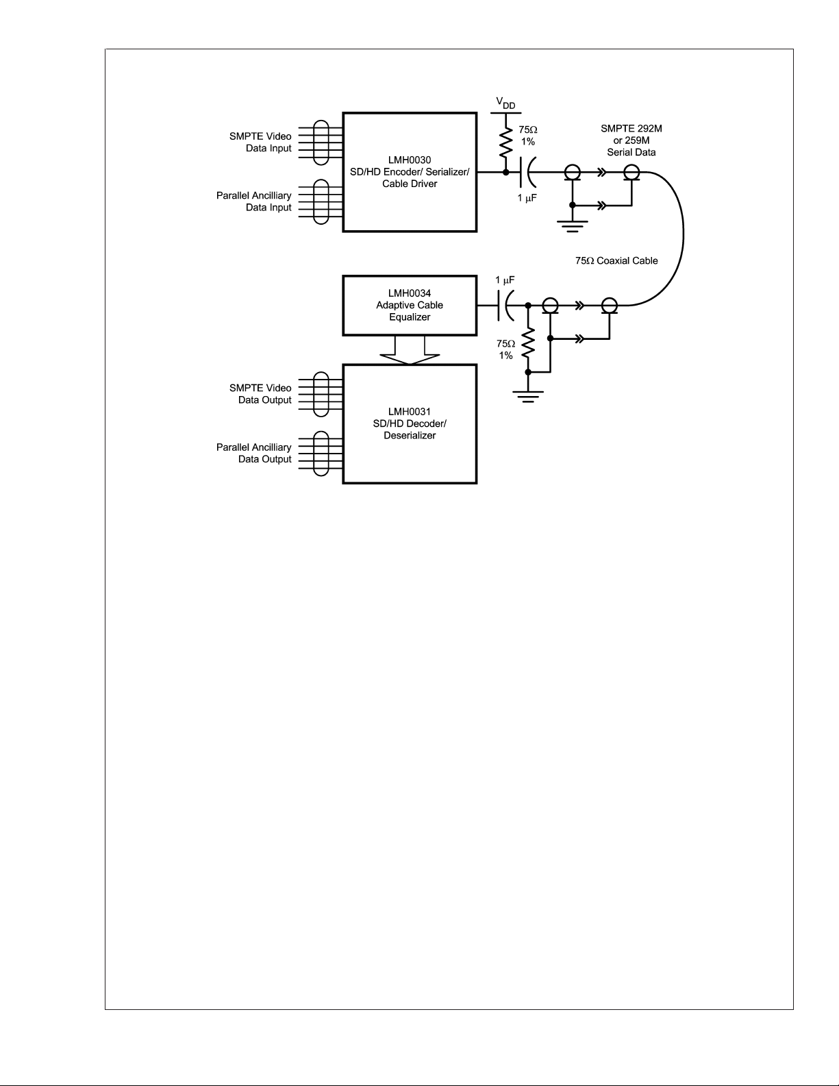
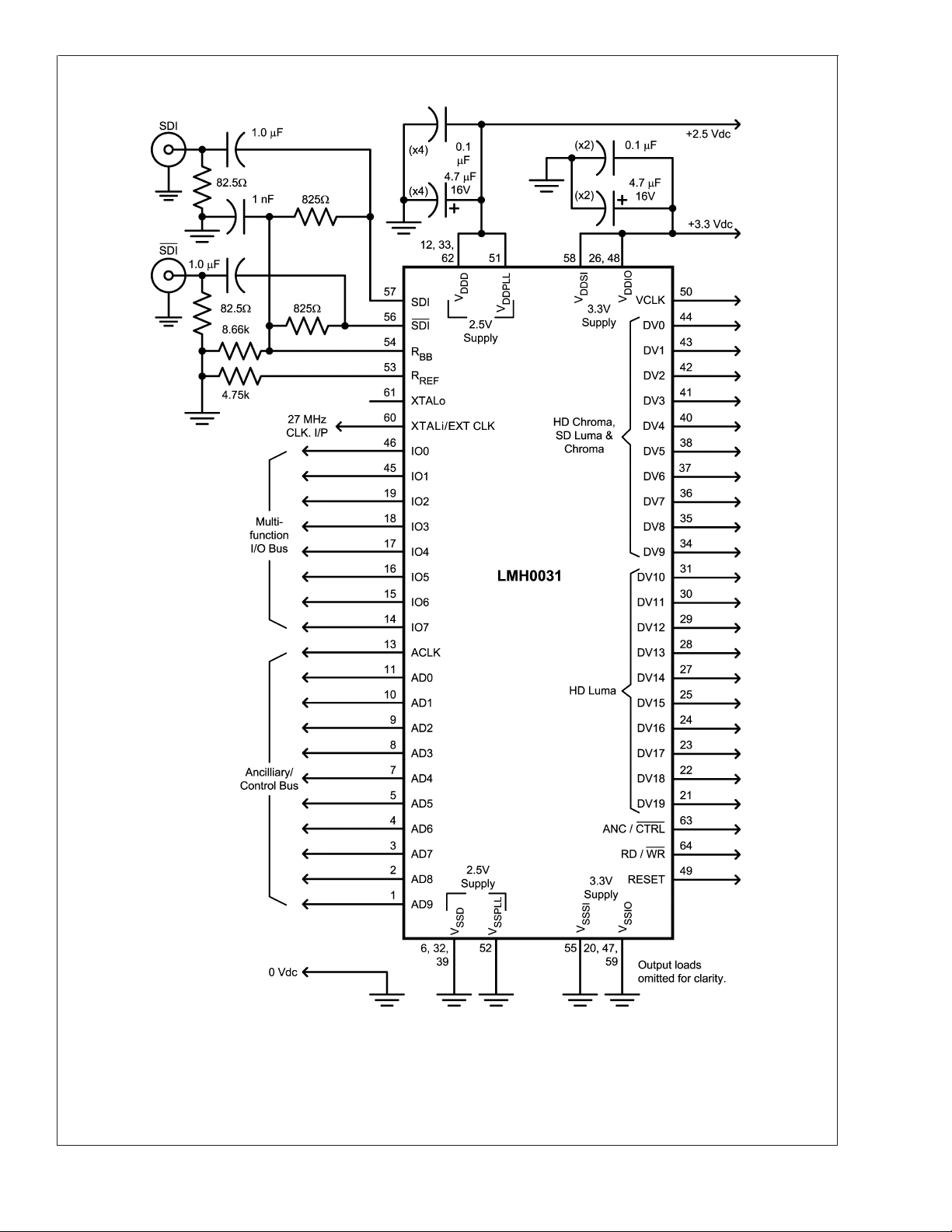
Typical Application
LMH0031
20179601
www.national.com 2
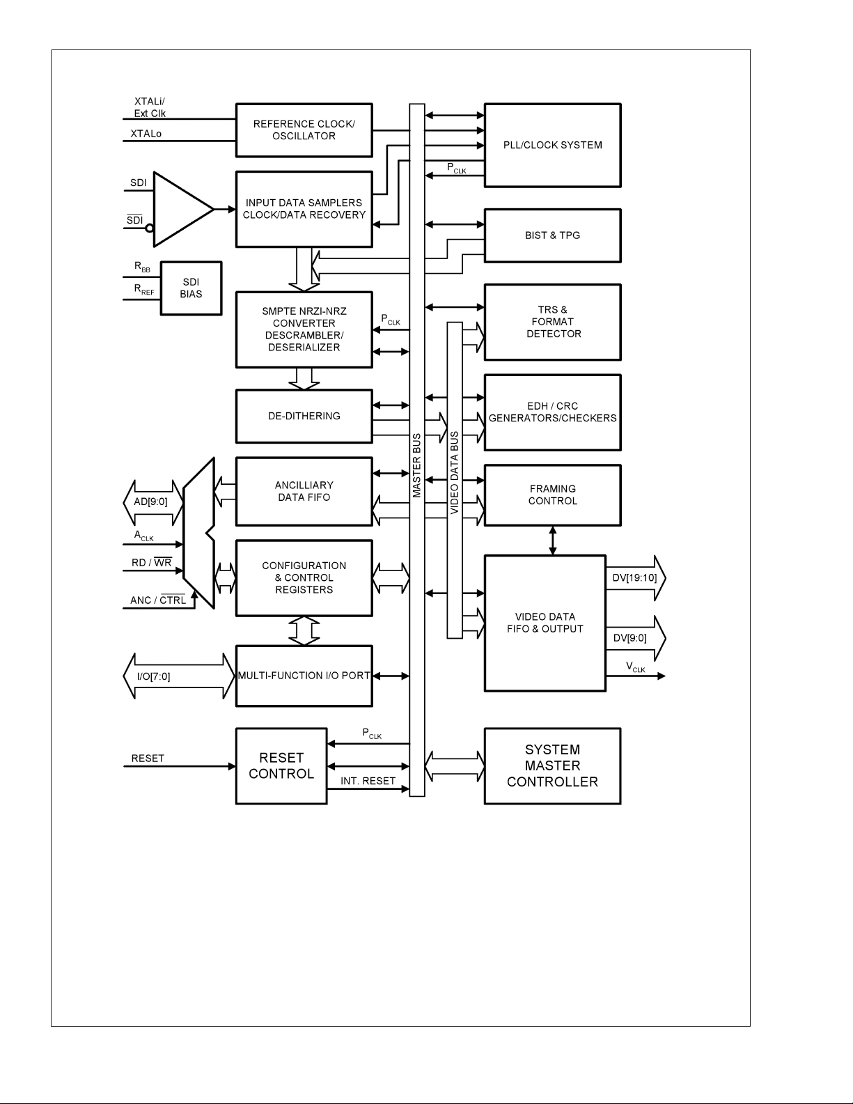
Block Diagram
LMH0031
20179602
www.national.com3
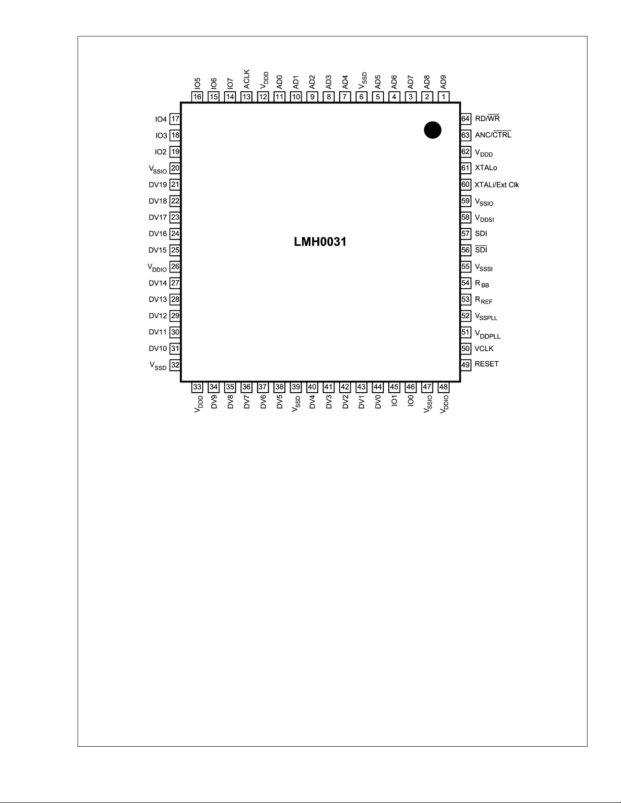
Connection Diagram
LMH0031
64-Pin TQFP
Order Number LMH0031VS
See NS Package Number VEC-64A
20179603
www.national.com 4
LMH0031
Absolute Maximum Ratings (Note 1)
It is anticipated that this device will not be offered in
a military qualified version. If Military/Aerospace speci-
fied devices are required, please contact the National
Semiconductor Sales Office / Distributors for availability
and specifications.
CMOS I/O Supply Voltage
(V
DDIO–VSSIO
SDI Supply Voltage
(V
DDSI–VSSSI
Digital Logic Supply Voltage
(V
DDD–VSSD
PLL Supply Voltage
(V
DDPLL–VSSPLL
CMOS Input Voltage
(Vi):
CMOS Output Voltage
(Vo):
): 4.0V
): 4.0V
): 3.0V
): 3.0V
V
−0.15V to
SSIO
+0.15V
V
DDIO
V
−0.15V to
SSIO
+0.15V
V
DDIO
CMOS Input Current (single input):
Vi=V
Vi=V
CMOS Output Source/Sink Current:
I
Output Current: +300 µA
BB
I
Output Current: +300 µA
REF
SDI Input Voltage
(Vi):
−0.15V: −5 mA
SSIO
+0.15V: +5 mA
DDIO
V
SSSI
V
±
−0.15V to
+0.15V
DDSI
6mA
Package Thermal Resistance
@
θ
0 LFM Airflow 40.1˚C/W
JA
@
θ
500 LFM Airflow 24.5˚C/W
JA
θ
JC
5.23˚C/W
Storage Temp. Range: −65˚C to +150˚C
Junction Temperature: +150˚C
Lead Temperature (Soldering 4
Sec): +260˚C
ESD Rating (HBM): 6.0 kV
ESD Rating (MM): 400 V
Recommended Operating Conditions
Symbol Parameter Conditions Reference Min Typ Max Units
V
V
V
V
T
DDIO
DDSD
DDD
DDPLL
A
CMOS I/O Supply Voltage V
SDI Supply Voltage V
Digital Logic Supply
Voltage
PLL Supply Voltage V
Operating Free Air
Temperature
DDIO−VSSIO
DDSI−VSSSI
V
DDD–VSSD
DDPLL–VSSPLL
3.150 3.300 3.450 V
2.375 2.500 2.625 V
0 +70 ˚C
Required Input Conditions
(Note 9)
Symbol Parameter Conditions Reference Min Typ Max Units
V
IN
t
r,tf
BR
V
CM(SDI)
V
IN(SDI)
V
IN(SDI)
tr,t
SDI
f
Input Voltage Range
Rise Time, Fall Time 10%–90% 1.0 1.5 3.0 ns
All LVCMOS
Inputs
SMPTE 259M, Level C
V
SSIO
V
DDIO
270
SMPTE 259M, Level D 360
Serial Input Data Rate
SMPTE 344M 540
SDI, SDI
M
SMPTE 292M 1,483
SMPTE 292M 1,485
Common Mode Voltage VIN= 125 mV
SDI Serial Input Voltage,
Single-ended
SDI Serial Input Voltage,
Differential
20%–80%, SMPTE 259M
Rise Time, Fall Time
Data Rates
20%–80%, SMPTE 292M
Data Rates
P-P
SDI, SDI
V
SSSI
+1.0V
125 800 880 mV
125 800 880 mV
0.4 1.0 1.5 ns
V
DDSI
−0.05V
270 ps
V
BPS
V
P-P
P-P
www.national.com5
Required Input Conditions (Continued)
Symbol Parameter Conditions Reference Min Typ Max Units
LMH0031
f
ACLK
DC
ACLK
tr,t
f
Ancillary / Control Data
Clock Frequency
Duty Cycle, Ancillary Clock 45 50 55 %
Ancillary / Control Clock
and Data Rise Time, Fall
10%–90% 1.0 1.5 3.0 ns
A
CLK
V
CLK
Time
t
S
t
H
R
REF
f
EXT CLK
f
XTAL
Setup Time, ADNto A
or IONto A
CLK
Edge
Hold Time, Rising Edge
to ADNor A
A
CLK
IO
N
Bias Supply Reference
Resistor
External Clock Frequency Ext Clk
Crystal Frequency Figure 6 XTALo, XTALi
Rising
CLK
CLK
3.0 1.5 ns
Control Data Input or
I/O Bus Input
to
IO
,ADN,A
N
CLK
Timing Diagram
3.0 1.5 ns
Tolerance 1% 4.75k Ω
−100
ppm
27.0
+100
ppm
DC Electrical Characteristics
Over Supply Voltage and Operating Temperature ranges, unless otherwise specified (Notes 2, 3).
Symbol Parameter Conditions Reference Min Typ Max Units
V
V
I
I
V
V
V
V
V
I
V
I
I
I
I
IH
IL
IH
IL
OH
OL
OHV
OLP
SDI
SDI
TH
BB
REF
DD
DD
(3.3V)
(2.5V)
Input Voltage High Level
Input Voltage Low Level V
Input Current High Level VIH=V
Input Current Low Level VIL=V
(Note 8) +85 +150
DDIO
SSIO
All LVCMOS
Inputs
Output Voltage High Level IOH=−2mA
Output Voltage Low Level IOL=+2mA V
All LVCMOS
Outputs
Minimum Dynamic V
Maximum Dynamic V
OH
OL
IOH=−2mA
(Note 6)
IOL=+2mA
(Note 6)
Serial Data Input Voltage
Serial Data Input Current
SDI, SDI
Input Thereshold Over VCM range
Bias Supply Output
Current
Reference Output Current R
Power Supply Current,
3.3V Supply, Total
Power Supply Current,
2.5V Supply, Total
= 8.66kΩ 1% −220 −188
R
BB
= 4.75kΩ 1% −290 −262
REF
270M
1,485M
270M
1,485M
Data Rate
BPS
Data Rate 47.0 50.0
BPS
Data Rate
BPS
Data Rate 220 340
BPS
V
DDIO,VDDSI
V
DDD,VDDPLL
2.0 V
SSIO
DDIO
0.8
−1 −20
2.4 2.7 V
V
SSIO
+0.3
V
SSIO
DDIO
DDIO
V
SSIO
+0.5V
−0.5
V
SSIO
+0.4
125 800 880 mV
±
1
<
100 mV
±
10 µA
38.0 45.0
80 120
MHz
MHz
V
µA
V
P-P
µA
mA
mA
www.national.com 6
AC Electrical Characteristics
Over Supply Voltage and Operating Temperature ranges, unless otherwise specified (Note 3).
Symbol Parameter Conditions Reference Min Typ Max Units
Serial Video Data Inputs
SMPTE 259M, Level C
SMPTE 259M, Level D 360
BR
SDI
Serial Input Data Rate
SMPTE 344M 540
SMPTE 292M 1,483
SDI, SDI
0.4 1.0 1.5 ns
t
r,tf
Rise Time, Fall Time
SMPTE 292M 1,485
20%–80%, SMPTE 259M
Data Rates
20%–80%, SMPTE 292M
Data Rates
Parallel Video Data Outputs
f
VCLK
t
pd
DC
SMPTE 259M, 270M
Video Output Clock
Frequency
SMPTE 267M, 360M
SMPTE 344M, 540M
SMPTE 292M, 1,483M
SMPTE 292M, 1,485M
Propagation Delay, Video
Clock to Video Data Valid
V
Duty Cycle, Video Clock V
50%–50%
BPS
BPS
BPS
V
BPS
BPS
V
Timing Diagram
CLK
CLK
CLK
to DV
N
27MHz
t
JIT
Video Data Output Clock
Jitter
36MHz 1.4
54MHz 1.0
V
CLK
74.25MHz 0.5
Parallel Ancillary / Control Data Inputs, Multi-function Parallel Bus Inputs
f
ACLK
DC
t
r,tf
t
S
t
H
A
Ancillary / Control Data
Clock Frequency
Duty Cycle, Ancillary Data
Clock
Output Rise Time, Fall
Time
Setup Time, ADNto A
or IONto A
CLK
CLK
Rising Edge
Hold Time, Rising Edge
A
IO
CLK
N
to ADNor A
CLK
to
ANC Data clock
(Note 7)
10%–90%
Control Data Input or I/O
Bus Input
A
CLK
,ADN,A
IO
N
CLK
Timing Diagram
45 50 55 %
1.0 1.5 3.0
3.0 1.5
3.0 1.5
Parallel Ancillary / Control Data Outputs
t
pd
t
pd
Propagation Delay, Clock
to Control Data
Propagation Delay, Clock
to Ancillary Data
50%–50%
to AD
A
CLK
N
Timing Diagram
Multi-function Parallel I/O Bus
t
r,tf
Rise Time, Fall Time 10%–90%
IO0–IO7
Timing Diagram
1.0 1.5 3.0 ns
PLL/CDR, Format Detect
t
LOCK
t
FORMAT
Note 1: “Absolute Maximum Ratings” are those parameter values beyond which the life and operation of the device cannot be guaranteed. The stating herein of
these maximums shall not be construed to imply that the device can or should be operated at or beyond these values. The table of “Electrical Characteristics”
specifies acceptable device operating conditions.
Lock Detect Time
Format Detect Time All Rates 20
SD Rates (Note 5) 0.32 1.0
270
M
270 ps
27.0
36.0
54.0
MHz
74.176
74.25
0.5 2.0 ns
50±5%
2.0
ns
V
CLK
MHz
8.5
11.5
LMH0031
BPS
P-P
ns
ns
msHD Rates (Note 5) 0.26 1.0
www.national.com7
AC Electrical Characteristics (Continued)
Note 2: Current flow into device pins is defined as positive. Current flow out of device pins is defined as negative. All voltages are referenced to V
V
=0V.
SSSI
LMH0031
Note 3: Typical values are stated for V
Note 4: Spec. is guaranteed by design.
Note 5: Measured from rising-edge of first SDI cycle until Lock Detect bit goes high (true). Lock time includes CDR phase acquisition time plus PLL lock time.
Note 6: V
simultaneous output switching conditions. V
conditions.
Note 7: When used to clock control data into or from the LMH0031, the duty cycle restriction does not apply.
Note 8: I
Note 9: Required Input Conditions are the electrical signal conditions or component values which shall be supplied by the circuit in which this device is used in order
for it to produce the specified DC and AC electrical output characteristics.
Note 10: Functional and certain other parametric tests utilize a LMH0030 as the input source to the SDI inputs of the LMH0031. The LMH0030 is DC coupled to
the inputs of the LMH0031. Typical V
and V
OHV
includes static current required by input pull-down devices.
IH
are measured with respect to reference ground. V
OLP
DDIO=VDDSI
= 800 mV, VCM= 2.9 V.
IN
= +3.3V, V
is the lowest output HIGH voltage or output droop that may occur under dynamic simultaneous output switching
OHV
DDD=VDDPLL
= +2.5V and TA= +25˚C.
is the peak output LOW voltage or ground bounce that may occur under dynamic
OLP
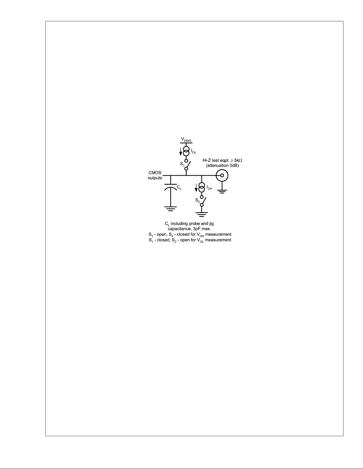
Test Loads
SSIO=VSSD
=
20179604
www.national.com 8
Test Circuit
LMH0031
20179607
www.national.com9
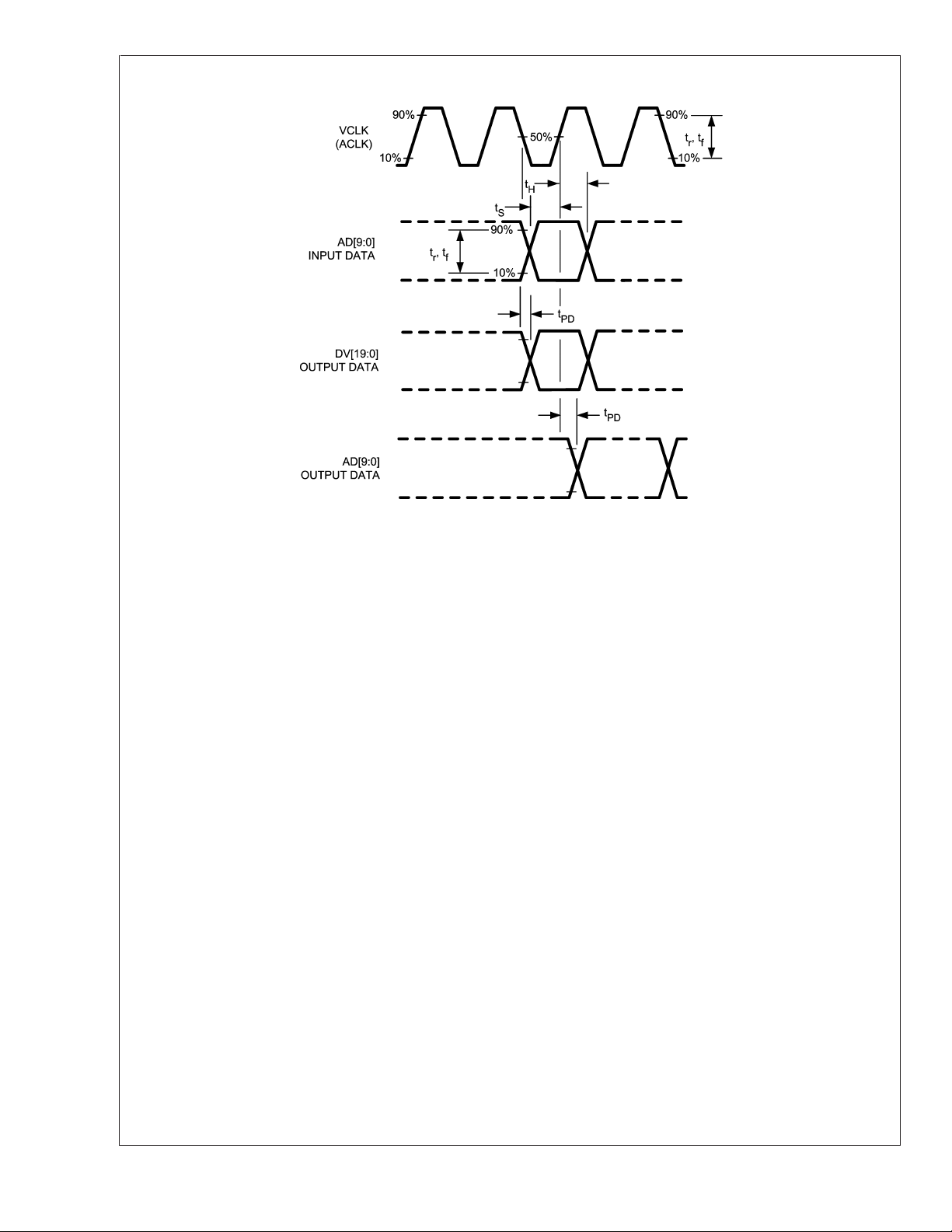
Timing Diagram
LMH0031
20179608
Device Operation
INTRODUCTION
The LMH0031 SMPTE 292M/259M Digital Video
Deserializer/Decoder is used in digital video signal origination and destination equipment: cameras, video tape recorders, telecines, editors, standards converters, video test and
other equipment. It decodes and converts serial SDTV or
HDTV component digital video signals into parallel format.
The LMH0031 decoder/deserializer processes serial digital
video (SDV) signals conforming to SMPTE 259M, SMPTE
344M (proposed) or SMPTE 292M and operates at serial
data rates of 270 Mbps, 360 Mbps, 540 Mbps, 1.483 Gbps
and 1.485 Gbps. Corresponding parallel output data rates
are 27.0 MHz, 36.0 MHz, 54.0 MHz, 74.176MHz and
74.25 MHz.
The LMH0031 accepts ECL or LVDS serial data input sig-
nals. Outputs signals are compatible with LVCMOS logic
devices.
Note: In the following explanations, these logical equivalences are observed: ON
≡
and OFF
Disabled≡Reset≡False≡Logic_0.
≡
Enabled≡Set≡True≡Logic_1
VIDEO DATA PATH
The Serial Data Inputs (SDI) accept serial video data at
SMPTE 259M standard definition, SMPTE 344M (proposed)
or SMPTE 292M high-definition data rates. These inputs
accept standard ECL or LVDS signal levels and may be used
single-ended or differentially. Inputs may be DC or AC
coupled, as required, to devices and circuits supplying the
data. Recommended operating conditions and all input DC
and AC voltage and current specifications shall be observed
when designing the input coupling circuits.
For convenience, a reference bias source, pin name R
REF
sets the reference current available from the input bias
source, pin name R
is 4.75kΩ, 1%. RBBis provided so that the SDI inputs
R
REF
. The recommended nominal value of
BB
may be supplied DC bias voltage via external resistors when
the inputs are AC-coupled. The bias source should be
loaded with a resistance to the V
current available at R
input biasing scheme using R
is 200µA. Figure 1 shows a typical
BB
BB
supply. The source
SS
and R
REF
.
,
www.national.com 10
 Loading...