

查询LMH0002供应商
LMH0002
SMPTE 292M / 259M Serial Digital Cable Driver
LMH0002 SMPTE 292M / 259M Serial Digital Cable Driver
January 2006
General Description
The LMH0002 SMPTE 292M / 259M serial digital cable
driver is a monolithic, high-speed cable driver designed for
use in SMPTE 292M / 259M serial digital video and ITU-T
G.703 serial digital data transmission applications. The
LMH0002 drives 75Ω transmission lines (Belden 8281,
Belden 1694A or equivalent) at data rates up to 1.485 Gbps.
The LMH0002 provides two selectable slew rates for
SMPTE 259M and SMPTE 292M compliance. The output
voltage swing is adjustable via a single external resistor.
The LMH0002 is powered from a single 3.3V supply. Power
consumption is typically 125mW in SD mode and 149mW in
HD mode.
Features
n SMPTE 292M, SMPTE 344M and SMPTE 259M
compliant
n Data rates to 1.485 Gbps
n Differential input
n 75Ω differential output
n Selectable slew rate
n Adjustable output amplitude
n Single 3.3V supply operation
n Operating temperature range: Commercial 0˚C to +70˚C
(LMH0002MA) or Industrial −40˚C to +85˚C
(LMH0002TMA)
n Typical power consumption: 125mW in SD mode and
149mW in HD mode
n Replaces the GS1528 and GS1528A
Applications
n SMPTE 292M, SMPTE 344M, and SMPTE 259M serial
digital interfaces
n Sonet/SDH and ATM interfaces
n Digital routers and switches
n Distribution amplifiers
n Buffer applications
n Set top boxes
n Security cameras
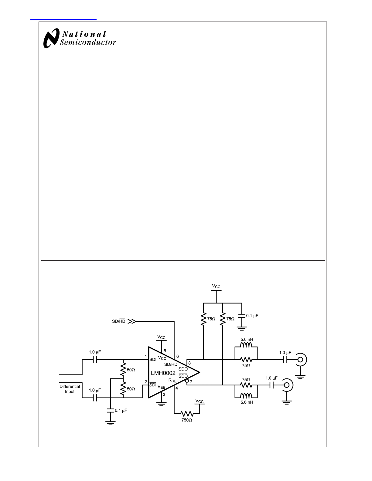
Typical Application
20176102
© 2006 National Semiconductor Corporation DS201761 www.national.com
Absolute Maximum Ratings (Note 1)
Supply Voltage: −0.5V to 3.6V
LMH0002
Input Voltage (all inputs) −0.3V to V
Output Current 28mA
Storage Temperature Range −65˚C to +150˚C
Junction Temperature +150˚C
Lead Temperature
(Soldering 4 Sec) +260˚C
Package Thermal Resistance
θ
8-pin SOIC
JA
8-pin SOIC
θ
JC
+0.3V
CC
+125˚C/W
+105˚C/W
ESD Rating (HBM) 5kV
ESD Rating (MM) 250V
Recommended Operating
Conditions
Supply Voltage (VCC–VEE): 3.3V±5%
Operating Free Air Temperature (T
LMH0002MA
LMH0002TMA
)
A
0˚C to +70˚C
−40˚C to +85˚C
DC Electrical Characteristics
Over Supply Voltage and Operating Temperature ranges, unless otherwise specified (Notes 2, 3).
Symbol Parameter Conditions Reference Min Typ Max Units
V
CMIN
V
SDI
V
CMOUT
V
SDO
I
CC
Input Common Mode Voltage SDI, SDI 1.6 +
/2
V
SDI
Input Voltage Swing Differential 100 2000 mV
Output Common Mode Voltage SDO, SDO VCC–
V
SDO
Output Voltage Swing Single-ended, 75Ω load,
= 750Ω 1%
R
REF
Single-ended, 75Ω load,
= 590Ω 1%
R
REF
750 800 850 mV
900 1000 1100 mV
SD/HD Input Voltage Min for SD SD/HD 2.4 V
Max for HD 0.8 V
SD/HD Input Current
3.7 µA
Supply Current SD/HD = 0, (Note 5) 45 49 mA
SD/HD = 1, (Note 5)
38 43 mA
V
–
CC
/2
V
SDI
V
P−P
V
P-P
P-P
AC Electrical Characteristics
Over Supply Voltage and Operating Temperature ranges, unless otherwise specified (Note 3).
Symbol Parameter Conditions Reference Min Typ Max Units
DR
t
jit
tr,t
t
OS
RL
Input Data Rate (Note 4) SDI, SDI 1485 Mbps
SDI
Additive Jitter 1.485 Gbps SDO, SDO 26 ps
270 Mbps 18 ps
Output Rise Time, Fall Time SD/HD = 0, 20% – 80%,
f
(Note 6)
SD/HD = 1, 20% – 80%
400 560 800 ps
120 220 ps
P-P
P-P
Mismatch in Rise/Fall Time (Note 4) 30 ps
Output Overshoot (Note 4) 8 %
Output Return Loss (Note 7) 15 20 dB
SDO
Note 1: "Absolute Maximum Ratings" are those parameter values beyond which the life and operation of the device cannot be guaranteed. The stating herein of
these maximums shall not be construed to imply that the device can or should be operated at or beyond these values. The table of "Electrical Characteristics"
specifies acceptable device operating conditions.
Note 2: Current flow into device pins is defined as positive. Current flow out of device pins is defined as negative. All voltages are stated referenced to V
Note 3: Typical values are stated for V
Note 4: Specification is guaranteed by characterization.
Note 5: Maximum I
Note 6: Specification is guaranteed by characterization and verified by test.
Note 7: Output return loss is dependent on board design. The LMH0002 meets this specification on the SD002 evaluation board from 5MHz to 1.5GHz.
is measured at VCC= +3.465V and TA= +70˚C.
CC
= +3.3V and TA= +25˚C.
CC
= 0 Volts.
EE
www.national.com 2

Connection Diagram
LMH0002
Order Number LMH0002MA or LMH0002TMA
See NS Package Number M08A
Pin Descriptions
Pin # Name Description
1 SDI Serial data true input.
2 SDI
3V
4R
5V
EE
REF
CC
6 SD/HD
Serial data complement input.
Negative power supply (ground).
Output driver level control. Connect a resistor to VCCto set output voltage swing.
Positive power supply (+3.3V).
Output slew rate control. Output rise/fall time complies with SMPTE 292M when low and
SMPTE 259M when high.
7 SDO Serial data complement output.
8 SDO Serial data true output.
Device Operation
INPUT INTERFACING
The LMH0002 accepts either differential or single-ended
input. The inputs are self-biased, allowing for simple AC or
DC coupling. DC-coupled inputs must be kept within the
specified common-mode range. SDI and SDI are self-biased
at approximately 2.1V with VCC= 3.3V. Figure 1 shows the
differential input stage for SDI and SDI.
8-Pin SOIC
20176101
20176104
FIGURE 1. Differential Input Stage for SDI and SDI.
www.national.com3

Device Operation (Continued)
OUTPUT INTERFACING
LMH0002
The LMH0002 uses current mode outputs. Single-ended
output levels are 800 mV
cable (with R
value of the R
The R
REF
the R
REF
below the R
= 750Ω). Output level is controlled by the
REF
resistor connected between pin 4 and VCC.
REF
resistor should be placed as close as possible to
pin. In addition, the copper in the plane layers
network should be removed to minimize
REF
parasitic capacitance.
into 75Ω AC-coupled coaxial
P-P
OUTPUT SLEW RATE CONTROL
The LMH0002 output rise and fall times are selectable for
either SMPTE 259M or SMPTE 292M compliance via pin 6,
SD/HD. For slower rise and fall times, or SMPTE 259M
compliance, SD/HD is set high. For faster rise and fall times,
or SMPTE 292M compliance, SD/HD is set low.
REPLACING THE GENNUM GS1528
The LMH0002 is form-fit-function compatible with the Gennum GS1528 and GS1528A.
www.national.com 4

Physical Dimensions inches (millimeters) unless otherwise noted
8-Pin SOIC
Order Number LMH0002MA or LMH0002TMA
NS Package Number M08A
LMH0002 SMPTE 292M / 259M Serial Digital Cable Driver
National does not assume any responsibility for use of any circuitry described, no circuit patent licenses are implied and National reserves
the right at any time without notice to change said circuitry and specifications.
For the most current product information visit us at www.national.com.
LIFE SUPPORT POLICY
NATIONAL’S PRODUCTS ARE NOT AUTHORIZED FOR USE AS CRITICAL COMPONENTS IN LIFE SUPPORT DEVICES OR SYSTEMS
WITHOUT THE EXPRESS WRITTEN APPROVAL OF THE PRESIDENT AND GENERAL COUNSEL OF NATIONAL SEMICONDUCTOR
CORPORATION. As used herein:
1. Life support devices or systems are devices or systems
which, (a) are intended for surgical implant into the body, or
(b) support or sustain life, and whose failure to perform when
properly used in accordance with instructions for use
2. A critical component is any component of a life support
device or system whose failure to perform can be reasonably
expected to cause the failure of the life support device or
system, or to affect its safety or effectiveness.
provided in the labeling, can be reasonably expected to result
in a significant injury to the user.
BANNED SUBSTANCE COMPLIANCE
National Semiconductor manufactures products and uses packing materials that meet the provisions of the Customer Products
Stewardship Specification (CSP-9-111C2) and the Banned Substances and Materials of Interest Specification (CSP-9-111S2) and contain
no ‘‘Banned Substances’’ as defined in CSP-9-111S2.
Leadfree products are RoHS compliant.
National Semiconductor
Americas Customer
Support Center
Email: new.feedback@nsc.com
Tel: 1-800-272-9959
www.national.com
National Semiconductor
Europe Customer Support Center
Fax: +49 (0) 180-530 85 86
Email: europe.support@nsc.com
Deutsch Tel: +49 (0) 69 9508 6208
English Tel: +44 (0) 870 24 0 2171
Français Tel: +33 (0) 1 41 91 8790
National Semiconductor
Asia Pacific Customer
Support Center
Email: ap.support@nsc.com
National Semiconductor
Japan Customer Support Center
Fax: 81-3-5639-7507
Email: jpn.feedback@nsc.com
Tel: 81-3-5639-7560
 Loading...