LME49870
44V Single High Performance, High Fidelity Audio
Operational Amplifier
LME49870 44V Single High Performance, High Fidelity Audio Operational Amplifier
January 14, 2008
General Description
The LME49870 is part of the ultra-low distortion, low noise,
high slew rate operational amplifier series optimized and fully
specified for high performance, high fidelity applications.
Combining advanced leading-edge process technology with
state-of-the-art circuit design, the LME49870 audio operational amplifier delivers superior audio signal amplification for
outstanding audio performance. The LME49870 combines
extremely low voltage noise density (2.7nV/√Hz
ishingly low THD+N (0.00003%) to easily satisfy the most
demanding audio applications. To ensure that the most challenging loads are driven without compromise, the LME49870
has a high slew rate of ±20V/μs and an output current capability of ±26mA. Further, dynamic range is maximized by an
output stage that drives 2kΩ loads to within 1V of either power
supply voltage and to within 1.4V when driving 600Ω loads.
The LME49870's outstanding CMRR (120dB), PSRR
(120dB), and VOS (0.1mV) give the amplifier excellent operational amplifier DC performance.
The LME49870 has a wide supply range of ±2.5V to ±22V.
Over this supply range the LME49870 maintains excellent
common-mode rejection, power supply rejection, and low input bias current. The LME49870 is unity gain stable. This
Audio Operational Amplifier achieves outstanding AC performance while driving complex loads with values as high as
100pF.
The LME49870 is available in 8–lead narrow body SOIC.
Demonstration boards are available for each package.
) with van-
Key Specifications
■ Power Supply Voltage Range ±2.5V to ±22V
■ THD+N
(AV = 1, V
OUT
= 3V
, fIN = 1kHz)
RMS
RL = 2kΩ
RL = 600Ω
0.00003% (typ)
0.00003% (typ)
■ Input Noise Density 2.7nV/√Hz (typ)
■ Slew Rate
■ Gain Bandwidth Product
■ Open Loop Gain (R
= 600Ω)
L
■ Input Bias Current
■ Input Offset Voltage
■ DC Gain Linearity Error
Features
Easily drives 600Ω loads
■
Optimized for superior audio signal fidelity
■
Output short circuit protection
■
PSRR and CMRR exceed 120dB (typ)
■
Applications
High quality audio amplification
■
High fidelity preamplifiers, phono preamps, and
■
multimedia
High performance professional audio
■
High fidelity equalization and crossover networks with
■
active filters
High performance line drivers and receivers
■
Low noise industrial applications including test,
■
measurement, and ultrasound
±20V/μs (typ)
55MHz (typ)
140dB (typ)
10nA (typ)
0.1mV (typ)
0.000009%
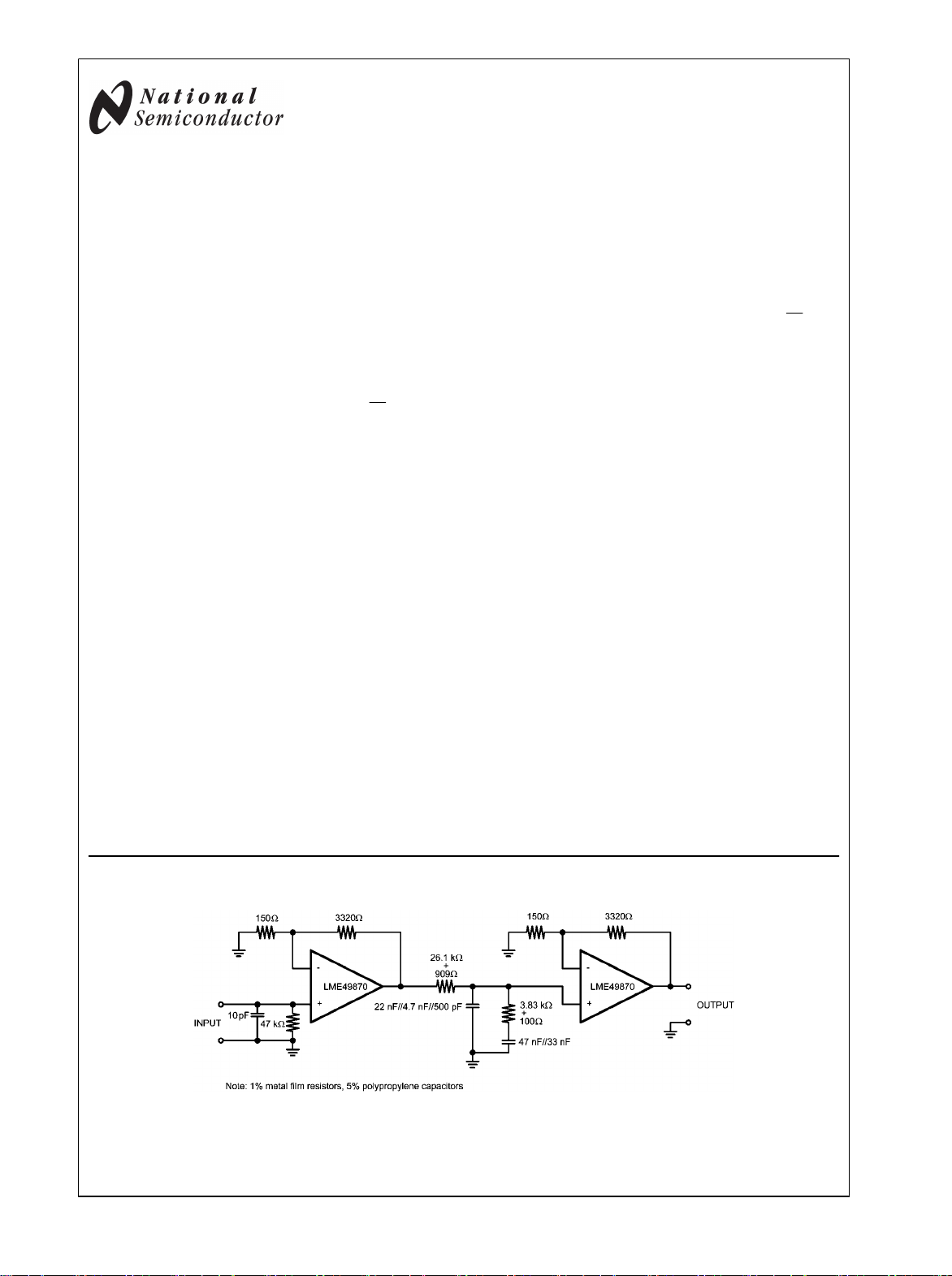
Typical Application
Passively Equalized RIAA Phono Preamplifier
© 2008 National Semiconductor Corporation 300194 www.national.com
300194k5
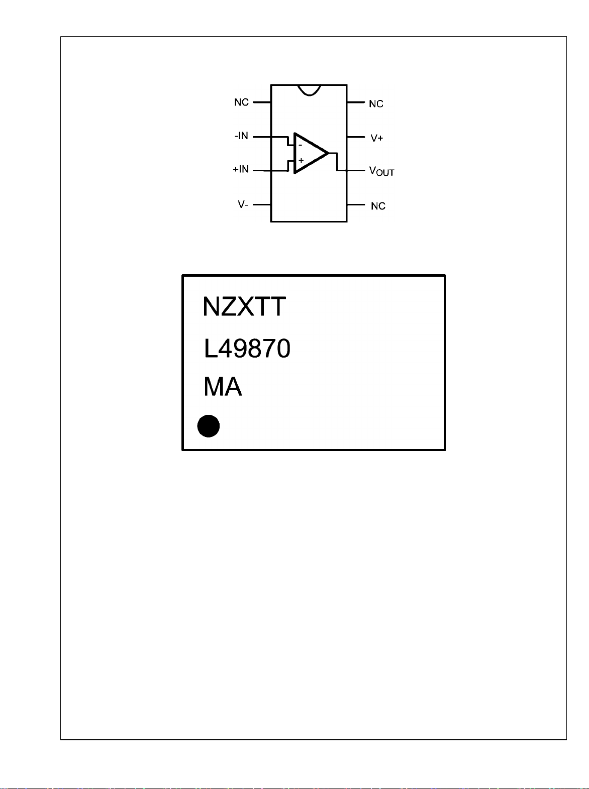
Connection Diagrams
LME49870
Order Number LME49870MA
30019401
See NS Package Number — M08A
LME49870 Top Mark
N — National Logo
Z — Assembly Plant code
X — 1 Digit Date code
TT — Die Traceability
L49870 — LME49870
MA — Package code
30019402
www.national.com 2
Absolute Maximum Ratings (Notes 1, 2)
If Military/Aerospace specified devices are required,
please contact the National Semiconductor Sales Office/
Distributors for availability and specifications.
Power Supply Voltage
(VS = V+ - V-)
Storage Temperature −65°C to 150°C
Input Voltage
(V-) - 0.7V to (V+) + 0.7V
Output Short Circuit (Note 3) Continuous
Power Dissipation Internally Limited
ESD Rating (Note 4) 2000V
ESD Rating (Note 5)
46V
Pins 1, 4, 7 and 8 200V
Pins 2, 3, 5 and 6 100V
Junction Temperature 150°C
Thermal Resistance
θJA (SO)
145°C/W
Operating Ratings
Temperature Range
T
≤ TA ≤ T
MIN
MAX
Supply Voltage Range
−40°C ≤ TA ≤ 85°C
±2.5V ≤ VS ≤ ±22V
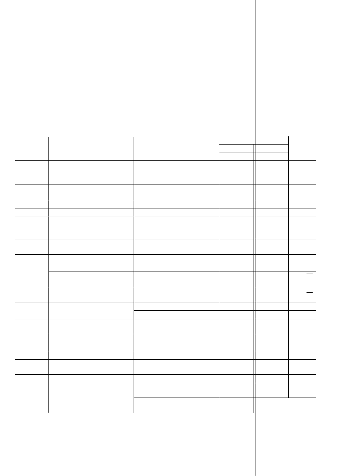
Electrical Characteristics for the LME49870 (Note 1) The following specifications apply for V
±18V and ±22V, RL = 2kΩ, R
Symbol Parameter Conditions
THD+N Total Harmonic Distortion + Noise
IMD Intermodulation Distortion
= 10Ω, fIN = 1kHz, TA = 25°C, unless otherwise specified.
SOURCE
AV = 1, V
OUT
= 3V
rms
RL = 2kΩ
RL = 600Ω
AV = 1, V
OUT
= 3V
RMS
Two-tone, 60Hz & 7kHz 4:1
LME49870
Typical Limit
(Note 6) (Note 7)
0.00003
0.00003 0.00009
0.00005 %
=
S
Units
(Limits)
% (max)
GBWP Gain Bandwidth Product 55 45 MHz (min)
SR Slew Rate ±20 ±15
V
FPBW Full Power Bandwidth
= 1V
OUT
referenced to output magnitude
P-P
, –3dB
10
V/μs (min)
MHz
at f = 1kHz
t
s
e
n
i
n
V
OS
ΔVOS/ΔTemp
PSRR
I
B
ΔIOS/ΔTemp
I
OS
V
IN-CM
Settling time
Equivalent Input Noise Voltage
Equivalent Input Noise Density
Current Noise Density
Offset Voltage
Average Input Offset Voltage Drift vs
Temperature
Average Input Offset Voltage Shift vs
Power Supply Voltage
AV = –1, 10V step, CL = 100pF
0.1% error range
fBW = 20Hz to 20kHz
f = 1kHz
f = 10Hz
f = 1kHz
f = 10Hz
1.2
0.34 0.65
2.5
6.4
1.6
3.1
VS = ±18V ±0.12 mV (max)
VS = ±22V ±0.14 ±0.7 mV (max)
–40°C ≤ TA ≤ 85°C
VS = ±18V, ΔVS = 24V (Note 8)
VS = ±22V, ΔVS = 30V
0.1
120
120 110
Input Bias Current VCM = 0V 10 72 nA (max)
Input Bias Current Drift vs
Temperature
–40°C ≤ TA ≤ 85°C
0.2
Input Offset Current VCM = 0V 11 65 nA (max)
VS = ±18V
Common-Mode Input Voltage Range
VS = ±22V
+17.1
–16.9
+21.0
–20.8
μs
μV
(max)
4.7
nV/√Hz
(max)
pA/√Hz
μV/°C
dB (min)
nA/°C
V (min)
V (min)
RMS

Symbol Parameter Conditions
CMRR Common-Mode Rejection
Z
IN
A
VOL
R
L
V
OUTMAX
Differential Input Impedance
Common Mode Input Impedance –10V<Vcm<10V 1000
Open Loop Voltage Gain
Maximum Output Voltage Swing
VS = ±18V
–12V≤Vcm≤12V
VS = ±22V
–15V≤Vcm≤15V
VS = ±18V
–12V≤Vout≤12V
RL = 600Ω
RL = 2kΩ
RL = 10Ω
VS = ±22V
–15V≤Vout≤15V
RL = 600Ω
RL = 2kΩ
RL = 10Ω
RL = 600Ω
VS = ±18V
VS = ±22V
LME49870
Typical Limit
(Note 6) (Note 7)
Units
(Limits)
120 dB (min)
120 110 dB (min)
30
140
140
140
140
125
140
140
kΩ
MΩ
dB
dB
dB
dB
dB
dB
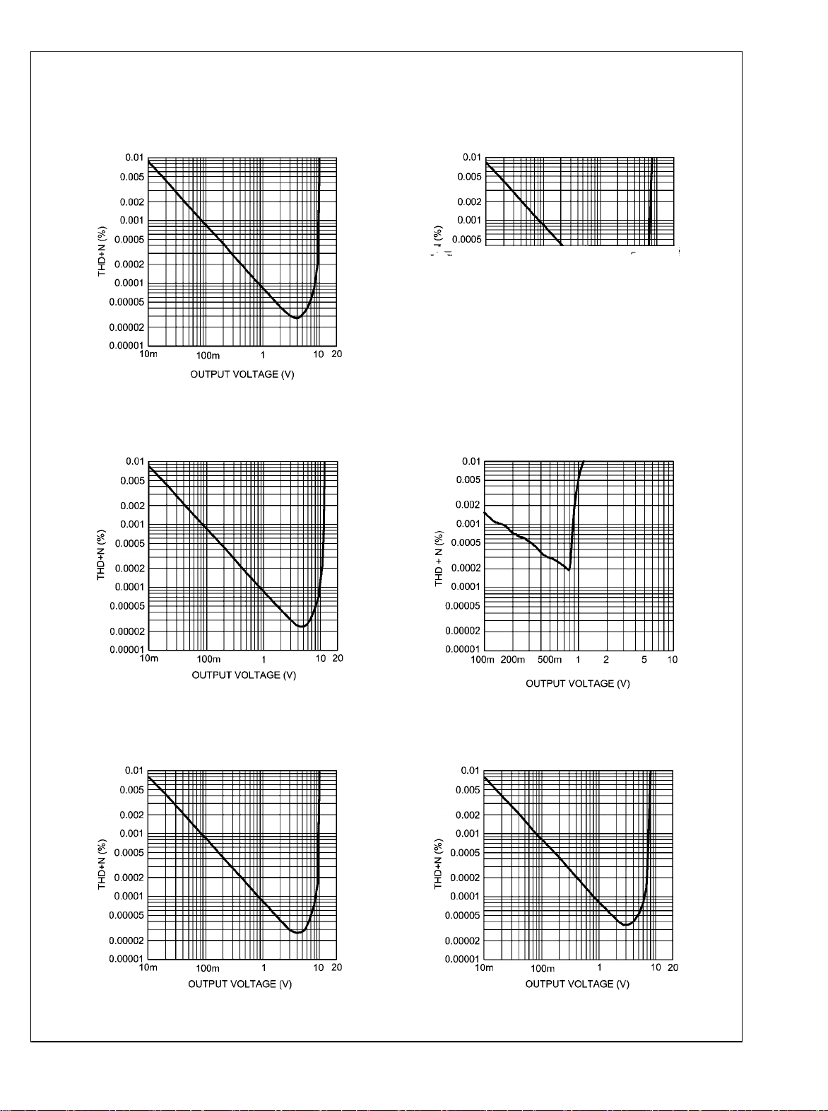
Typical Performance Characteristics
LME49870
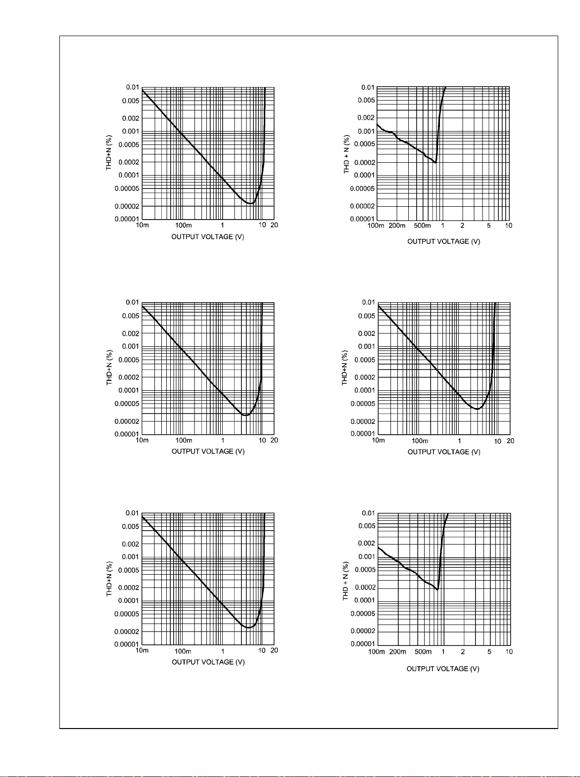
THD+N vs Output Voltage
VCC = 15V, VEE = –15V
RL = 2kΩ
THD+N vs Output Voltage
VCC = 22V, VEE = –22V
RL = 2kΩ
300194k6
THD+N vs Output Voltage
VCC = 12V, VEE = –12V
RL = 2kΩ
300194k7
THD+N vs Output Voltage
VCC = 2.5V, VEE = –2.5V
RL = 2kΩ
THD+N vs Output Voltage
VCC = 15V, VEE = –15V
RL = 600Ω
300194k8
300194k9
300194i4
THD+N vs Output Voltage
VCC = 12V, VEE = –12V
RL = 600Ω
300194l0
5 www.national.com
LME49870
THD+N vs Output Voltage
VCC = 22V, VEE = –22V
RL = 600Ω
THD+N vs Output Voltage
VCC = 2.5V, VEE = –2.5V
RL = 600Ω
THD+N vs Output Voltage
VCC = 15V, VEE = –15V
RL = 10kΩ
THD+N vs Output Voltage
VCC = 22V, VEE = –22V
RL = 10kΩ
300194l1
300194l2
300194i6
THD+N vs Output Voltage
VCC = 12V, VEE = –12V
RL = 10kΩ
300194l3
THD+N vs Output Voltage
VCC = 2.5V, VEE = –2.5V
RL = 10kΩ
300194l4
www.national.com 6
300194i5
LME49870
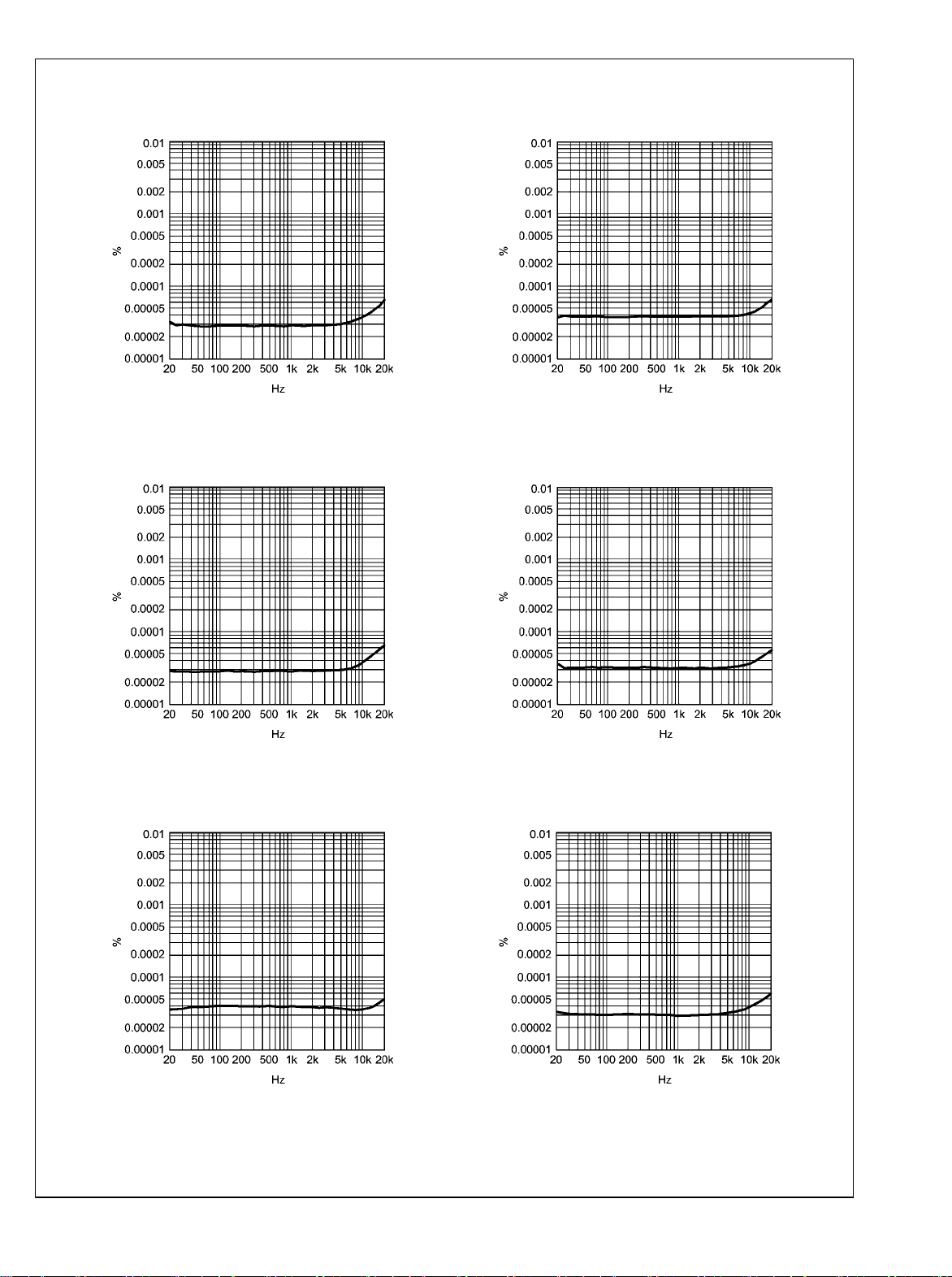
THD+N vs Frequency
VCC = 15V, VEE = –15V, V
RL = 2kΩ
THD+N vs Frequency
VCC = 22V, VEE = –22V, V
RL = 2kΩ
OUT
OUT
= 3V
= 3V
RMS
RMS
30019463
THD+N vs Frequency
VCC = 12V, VEE = –12V, V
RL = 2kΩ
THD+N vs Frequency
VCC = 15V, VEE = –15V, V
RL = 600Ω
OUT
OUT
= 3V
= 3V
RMS
30019462
RMS
THD+N vs Frequency
VCC = 12V, VEE = –12V, V
RL = 600Ω
OUT
= 3V
RMS
30019464
300194k3
30019459
THD+N vs Frequency
VCC = 22V, VEE = –22V, V
OUT
= 3V
RMS
RL = 600Ω
30019460
7 www.national.com
LME49870
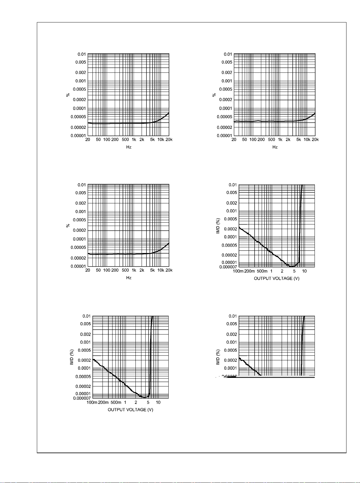
THD+N vs Frequency
VCC = 15V, VEE = –15V, V
RL = 10kΩ
OUT
= 3V
RMS
THD+N vs Frequency
VCC = 12V, VEE = –12V, V
RL = 10kΩ
OUT
= 3V
RMS
THD+N vs Frequency
VCC = 22V, VEE = –22V, V
RL = 10kΩ
IMD vs Output Voltage
VCC = 12V, VEE = –12V
RL = 2kΩ
OUT
= 3V
RMS
30019467
30019468
30019466
IMD vs Output Voltage
VCC = 15V, VEE = –15V
RL = 2kΩ
300194e6
IMD vs Output Voltage
VCC = 22V, VEE = –22V
RL = 2kΩ
300194e5
www.national.com 8
300194e7
LME49870
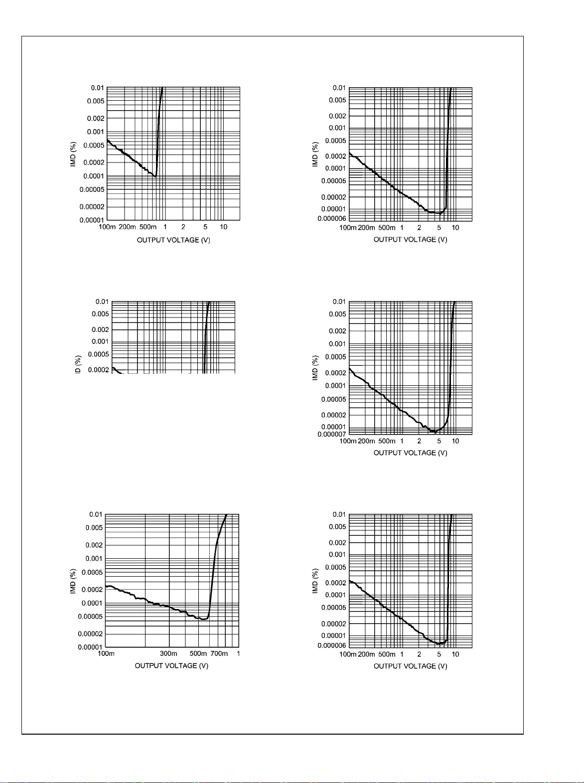
IMD vs Output Voltage
VCC = 2.5V, VEE = –2.5V
RL = 2kΩ
IMD vs Output Voltage
VCC = 12V, VEE = –12V
RL = 600Ω
300194e4
IMD vs Output Voltage
VCC = 15V, VEE = –15V
RL = 600Ω
300194e2
IMD vs Output Voltage
VCC = 22V, VEE = –22V
RL = 600Ω
IMD vs Output Voltage
VCC = 2.5V, VEE = –2.5V
RL = 600Ω
300194e0
300194e1
300194e3
IMD vs Output Voltage
VCC = 15V, VEE = –15V
RL = 10kΩ
300194f1
9 www.national.com
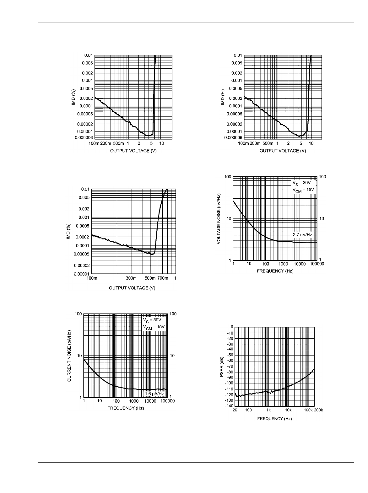
LME49870
IMD vs Output Voltage
VCC = 12V, VEE = –12V
RL = 10kΩ
IMD vs Output Voltage
VCC = 22V, VEE = –22V
RL = 10kΩ
300194f0
IMD vs Output Voltage
VCC = 2.5V, VEE = –2.5V
RL = 10kΩ
Current Noise Density vs Frequency
300194l6
300194f2
Voltage Noise Density vs Frequency
PSRR+ vs Frequency
VCC = 15V, VEE = –15V
RL = 2kΩ, V
RIPPLE
= 200mVpp
300194h6
300194h7
www.national.com 10
300194p7
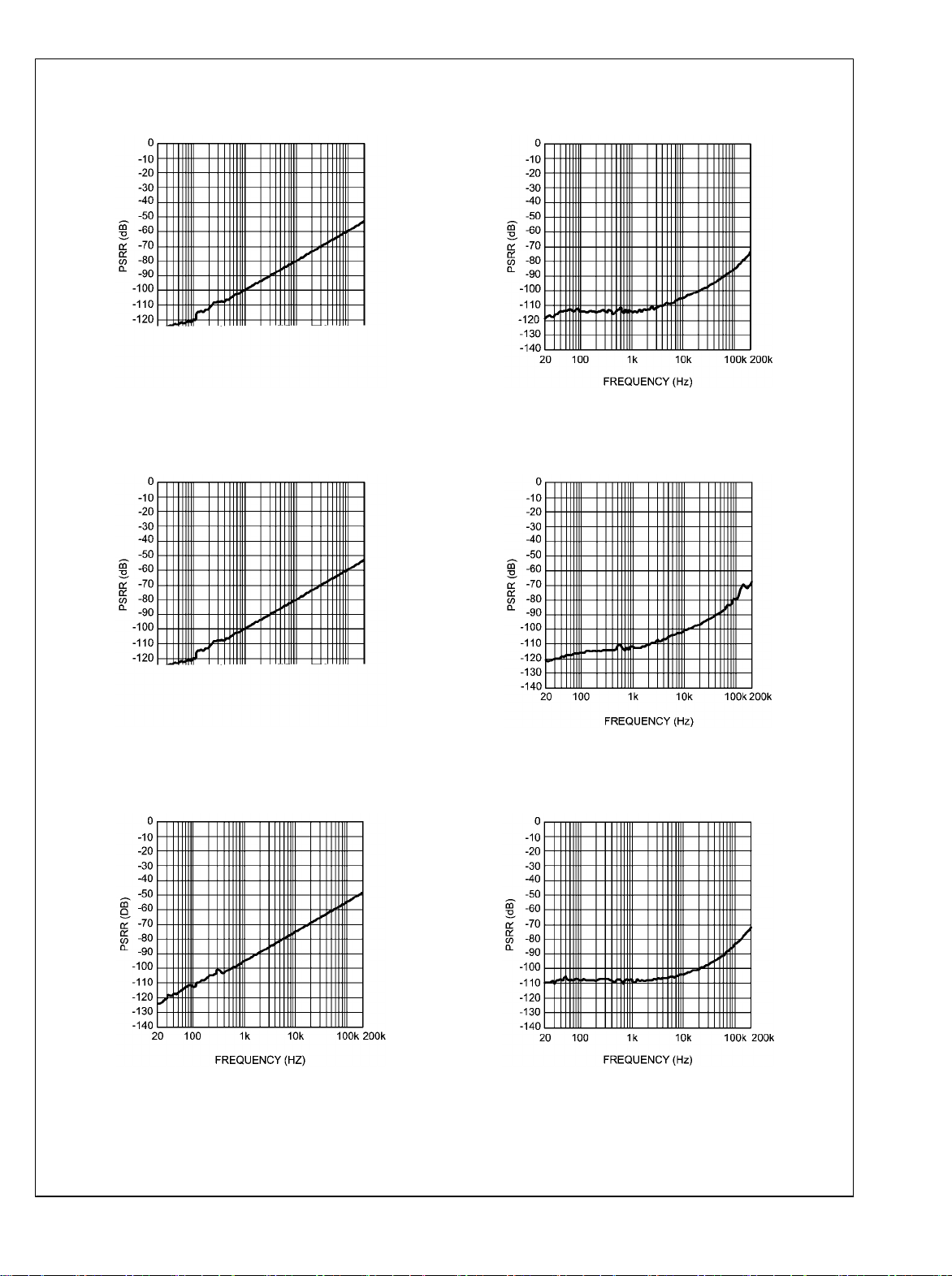
LME49870
PSRR- vs Frequency
VCC = 15V, VEE = –15V
RL = 2kΩ, V
RIPPLE
PSRR- vs Frequency
VCC = 17V, VEE = –17V
RL = 2kΩ, V
RIPPLE
= 200mVpp
= 200mVpp
300194r2
PSRR+ vs Frequency
VCC = 17V, VEE = –17V
RL = 2kΩ, V
RIPPLE
PSRR+ vs Frequency
VCC = 12V, VEE = –12V
RL = 2kΩ, V
RIPPLE
= 200mVpp
300194q0
= 200mVpp
PSRR- vs Frequency
VCC = 12V, VEE = –12V
RL = 2kΩ, V
RIPPLE
= 200mVpp
300194r2
300194q9
300194p4
PSRR+ vs Frequency
VCC = 22V, VEE = –22V
RL = 2kΩ, V
11 www.national.com
RIPPLE
= 200mVpp
300194q3
 Loading...