

January 4, 2008
LME49811 Audio Power Amplifier Series
High Fidelity 200 Volt Power Amplifier Input Stage with
Shutdown
General Description
The LME49811 is a high fidelity audio power amplifier input
stage designed for demanding consumer and pro-audio applications. Amplifier output power may be scaled by changing
the supply voltage and number of output devices. The
LME49811 is capable of driving an output stage to deliver in
excess of 500 watts single-ended into an 8 ohm load in the
presence of 10% high line headroom and 20% supply regulation.
The LME49811 includes thermal shut down circuitry that activates when the die temperature exceeds 150°C. The
LME49811's shutdown function when activated, forces the
LME49811 into shutdown state.
Key Specifications
■ Wide operating voltage range ±20V to ±100V
■ PSRR (f = DC) 115dB (typ)
■ THD+N (f = 1kHz) 0.00035% (typ)
■ Output Drive Current 9mA
Features
■
Very high voltage operation
■
Scalable output power
■
Minimum external components
■
External compensation
■
Thermal Shutdown
Applications
■
Powered subwoofers
■
Pro audio
■
Powered studio monitors
■
Audio video receivers
■
Guitar Amplifiers
■
High voltage industrial applications
Typical Application
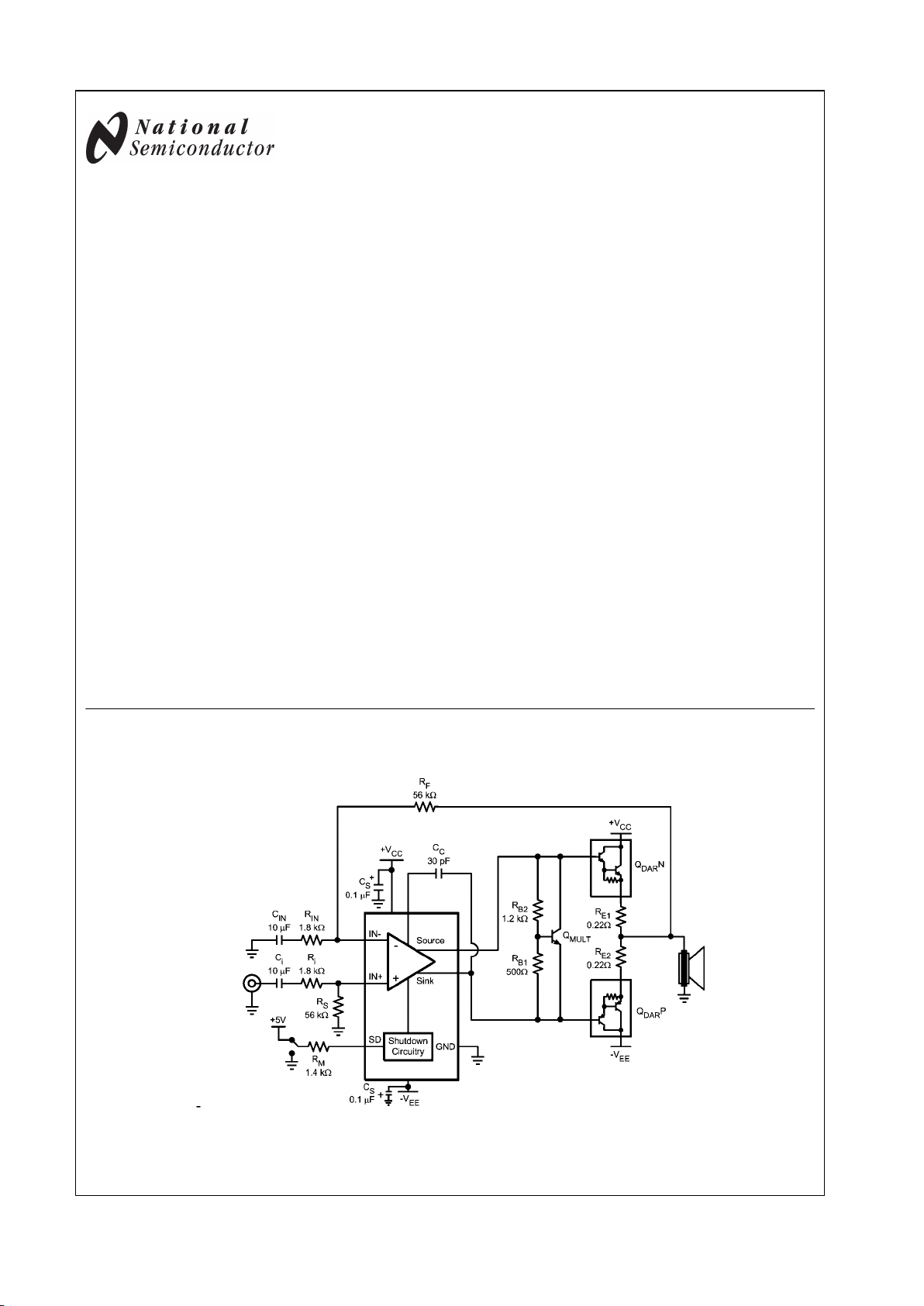
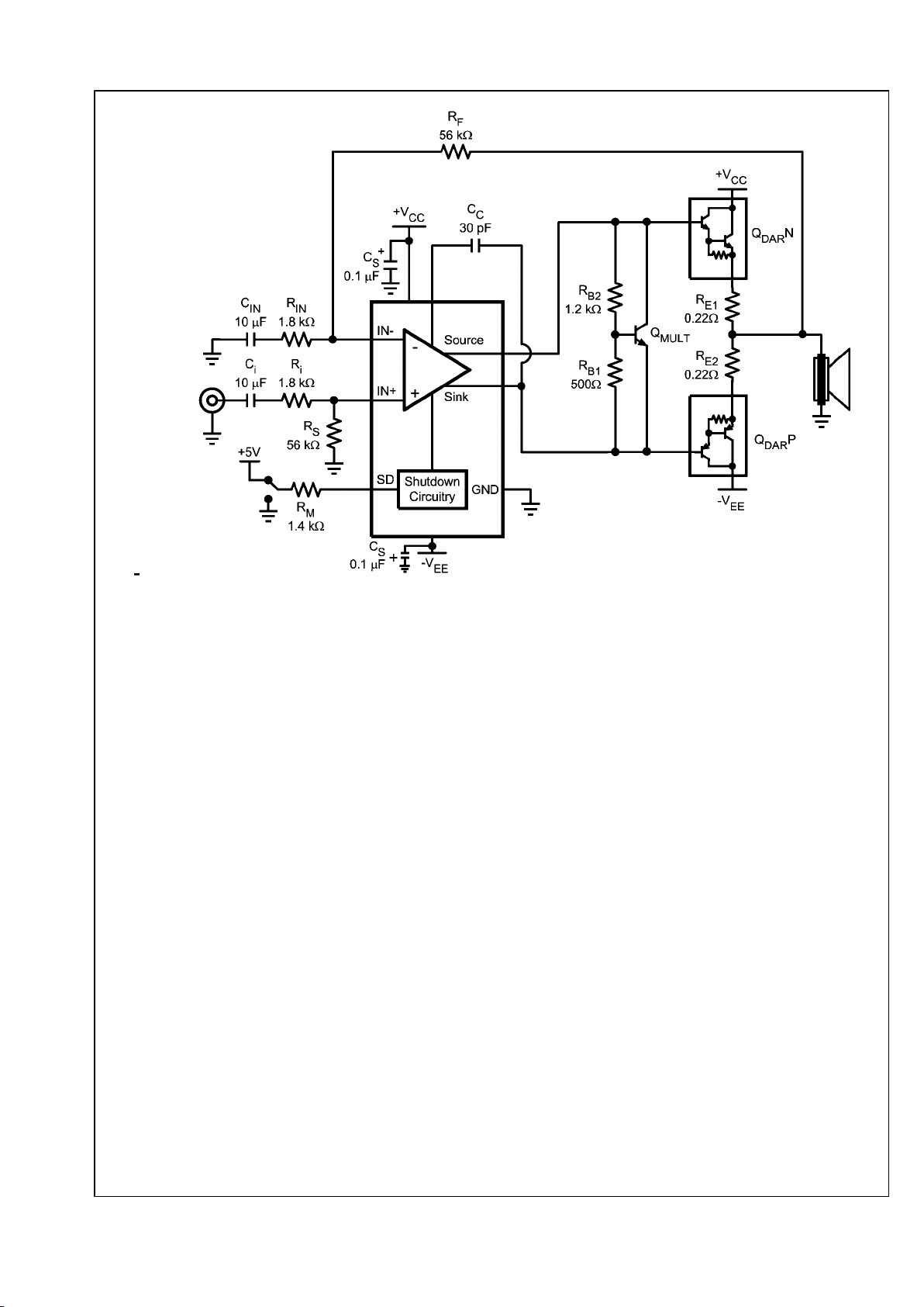
30004862
FIGURE 1. Typical Audio Amplifier Application Circuit
Overture® is a registered trademark of National Semiconductor Corporation.
© 2008 National Semiconductor Corporation 300048 www.national.com
LME49811 High Fidelity 200 Volt Power Amplifier Input Stage with Shutdown
30004862
Typical Audio Amplifier Application Circuit
www.national.com 2
LME49811
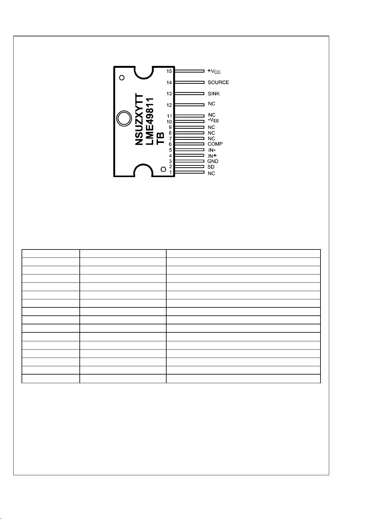
Connection Diagram
30004860
Top View
See Order Number LME49811TB
NS = National Logo
U = Fabrication plant code
Z = Assembly plant code
XY = 2 Digit date code
TT = Die traceability
TB = Package code
Pin Description
Pin Pin Name Description
1 NC No Connect, Pin electrically isolated
2 SD Shutdown Control
3 GND Device Ground
4 IN+ Non-Inverting Input
5 IN- Inverting Input
6 Comp External Compensation Connection
7 NC No Connect, Pin electrically isolated
8 NC No Connect, Pin electrically isolated
9 NC No Connect, Pin electrically isolated
10 -V
EE
Negative Power Supply
11 NC No Connect, Pin electrically isolated
12 NC No Connect, Pin electrically isolated
13 Sink Output Sink
14 Source Output Source
15 +V
CC
Positive Power Supply
3 www.national.com
LME49811
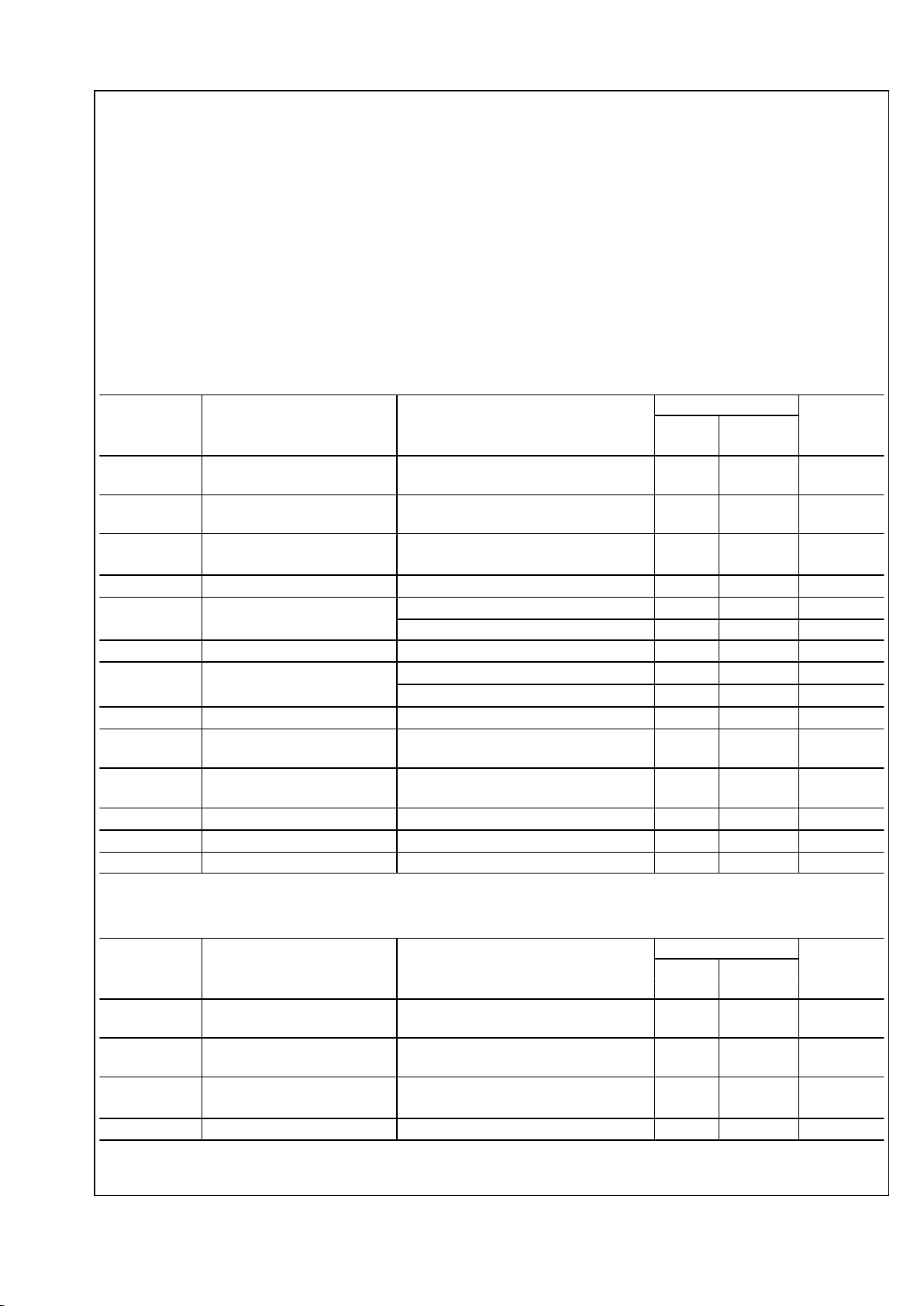
Absolute Maximum Ratings (Note 1)
If Military/Aerospace specified devices are required,
please contact the National Semiconductor Sales Office/
Distributors for availability and specifications.
Supply Voltage |V+| + |V-|
200V
Differential Input Voltage +/-6V
Common Mode Input Range 0.4 VEE to 0.4 V
CC
Power Dissipation (Note 3) 4W
ESD Rating(Note 4) 2kV
ESD Rating (Note 5) 200V
Junction Temperature (T
JMAX
) (Note 8)
150°C
Soldering Information
T Package (10 seconds) 260°C
Storage Temperature -40°C to +150°C
Thermal Resistance
θ
JA
73°C/W
θ
JC
4°C/W
Operating Ratings (Notes 1, 2)
Temperature Range
T
MIN
≤ TA ≤ T
MAX
−40°C ≤ TA ≤ +85°C
Supply Voltage |V+| + |V-|
+/-20V ≤ V
TOTAL
≤ +/-100V
Electrical Characteristics +VCC = -VEE = 50V (Notes 1, 2)
The following specifications apply for ISD = 1.5mA, Figure 1, unless otherwise specified. Limits apply for TA = 25°C, CC = 30pF.
Symbol Parameter Conditions LME49811 Units
(Limits)
Typical Limit
(Note 6) (Note 7)
I
CC
Total Quiescent Power Supply
Current
VCM = 0V, VO = 0V, IO = 0A
14 17 mA (max)
I
EE
Total Quiescent Power Supply
Current
VCM = 0V, VO = 0V, IO = 0A
16 19 mA (max)
THD+N
Total Harmonic Distortion +
Noise
No load, AV = 29dB
V
OUT
= 20V
RMS
, f = 1kHz
0.00055 0.0015 % (max)
A
V
Closed Loop Voltage Gain 26 dB (min)
A
V
Open Loop Gain
VIN = 1mV
RMS
, f = 1kHz
93 dB
f = DC 120 dB
V
OM
Output Voltage Swing THD+N = 0.05%, Freq = 20Hz to 20kHz 33 V
RMS
V
NOISE
Output Noise
LPF = 30kHz, Av = 29dB
100
μV
A-weighted 70 180
μV (max)
I
OUT
Output Current Outputs Shorted 8 6.5 mA(min)
I
SD
Current into Shutdown Pin To put part in “play” mode 1.5
1
2
mA(min)
mA (max)
SR Slew Rate
VIN = 1.2V
P-P
, f = 10kHz square Wave,
Outputs shorted
16 13
V/μs (min)
V
OS
Input Offset Voltage VCM = 0V, IO = 0mA 1 3 mV (max)
I
B
Input Bias Current VCM = 0V, IO = 0mA
100 nA
PSRR Power Supply Rejection Ratio DC, Input Referred 115 105 dB (min)
Electrical Characteristics +VCC = –VEE = 100V (Notes 1, 2)
The following specifications apply for ISD = 1.5mA, Figure 1, unless otherwise specified. Limits apply for TA = 25°C.
Symbol Parameter Conditions LME49811 Units
(Limits)
Typical Limit
(Note 6) (Note 7)
I
CC
Total Quiescent Power Supply
Current
VCM = 0V, VO = 0V, IO = 0A
17 22 mA (max)
I
EE
Total Quiescent Power Supply
Current
VCM = 0V, VO = 0V, IO = 0A
19 24 mA (max)
THD+N
Total Harmonic Distortion +
Noise
No load, AV = 30dB
V
OUT
= 30V
RMS
, f = 1kHz
0.00035 0.001 % (max)
A
V
Closed Loop Voltage Gain 26 dB (min)
www.national.com 4
LME49811
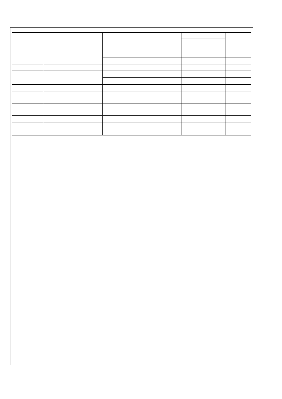
Symbol Parameter Conditions LME49811 Units
(Limits)
Typical Limit
(Note 6) (Note 7)
A
V
Open Loop Gain
VIN = 1mV
RMS
, f = 1kHz 93 dB
f = DC 120 dB
V
OM
Output Voltage Swing THD+N = 0.05%, Freq = 20Hz to 20kHz 68 V
RMS
V
NOISE
Output Noise
LPF = 30kHz, Av = 29dB 100
μV
A-weighted 70 180
μV (max)
I
OUT
Output Current Outputs Shorted 9 7 mA(min)
I
SD
Current into Shutdown Pin To put part in “play” mode 1.5
1
2
mA(min)
mA (max)
SR Slew Rate
VIN = 1.2V
P-P
, f = 10kHz square Wave,
Outputs shorted
17 14
V/μs (min)
V
OS
Input Offset Voltage VCM = 0V, IO = 0mA 1 3 mV (max)
I
B
Input Bias Current VCM = 0V, IO = 0mA
100 nA (max)
PSRR Power Supply Rejection Ratio f = DC, Input Referred 115 105 dB (min)
Note 1: “Absolute Maximum Ratings” indicate limits beyond which damage to the device may occur, including inoperability and degradation of device reliability
and/or performance. Functional operation of the device and/or non-degradation at the Absolute Maximum Ratings or other conditions beyond those indicated in
the Recommended Operating Conditions is not implied. The Recommended Operating Conditions indicate conditions at which the device is functional and the
device should not be operated beyond such conditions. All voltages are measured with respect to the ground pin, unless otherwise specified
Note 2: The Electrical Characteristics tables list guaranteed specifications under the listed Recommended Operating Conditions except as otherwise modified
or specified by the Electrical Characteristics Conditions and/or Notes. Typical specifications are estimations only and are not guaranteed.
Note 3: The maximum power dissipation must be derated at elevated temperatures and is dictated by T
JMAX
, θJA, and the ambient temperature, TA. The maximum
allowable power dissipation is P
DMAX
= (T
JMAX
- TA) / θJA or the number given in Absolute Maximum Ratings, whichever is lower.
Note 4: Human body model, applicable std. JESD22-A114C.
Note 5: Machine model, applicable std. JESD22-A115-A.
Note 6: Typical values represent most likely parametric norms at TA = +25ºC, and at the Recommended Operation Conditions at the time of product
characterization and are not guaranteed.
Note 7: Datasheet min/max specification limits are guaranteed by test or statistical analysis.
Note 8: The maximum operating junction temperature is 150°C.
Note 9: The Data taken with Bandwidth = 30kHz, AV = 29dB, CC = 30pF, and TA = 25°C except where specified.
5 www.national.com
LME49811
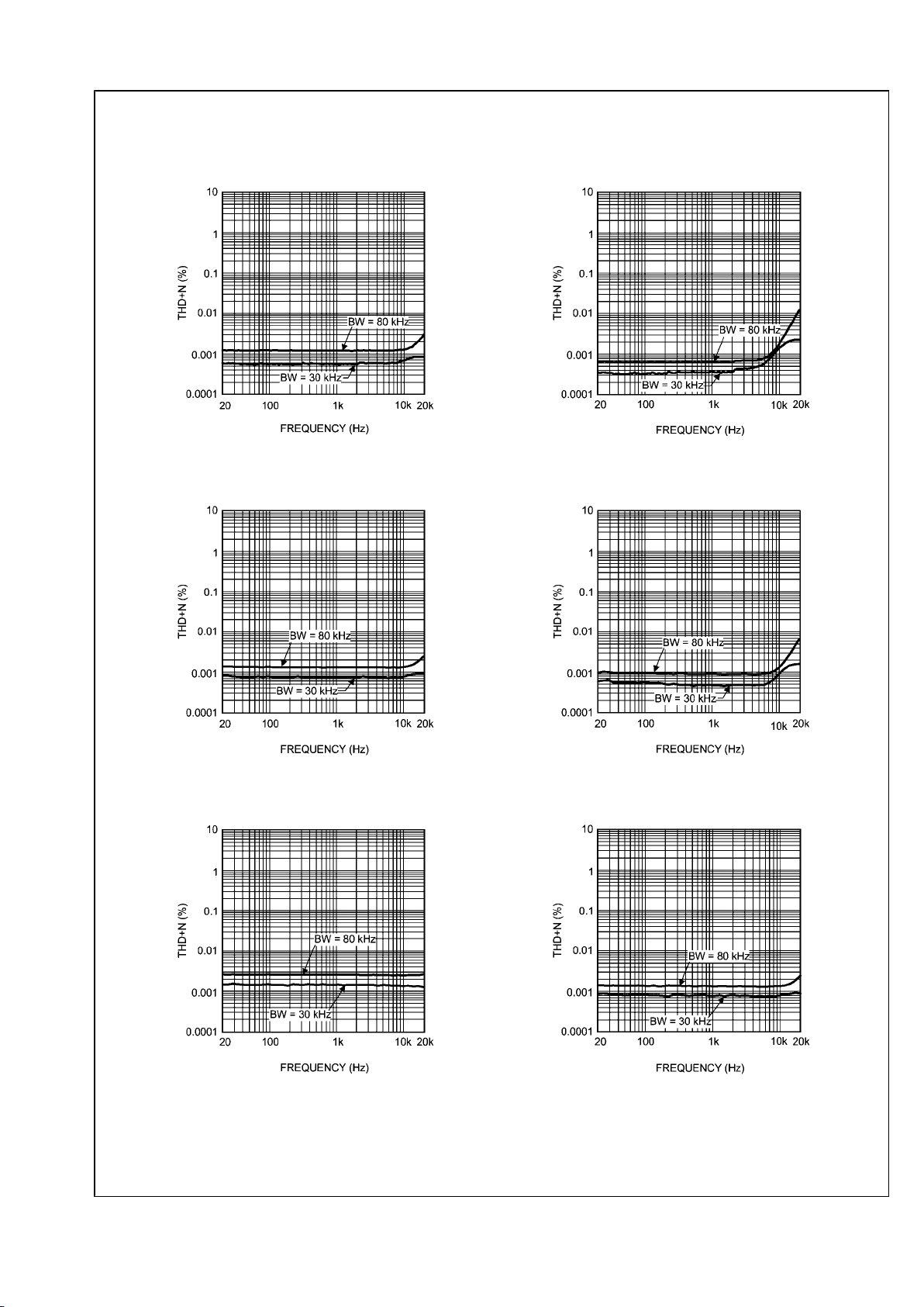
Typical Performance Characteristics for LME49811 (Note 9)
THD+N vs Frequency
+VCC = –VEE = 100V, VO = 14V
30004873
THD+N vs Frequency
+VCC = –VEE = 100V, VO = 30V
30004874
THD+N vs Frequency
+VCC = –VEE = 50V, VO = 10V
30004871
THD+N vs Frequency
+VCC = –VEE = 50V, VO = 20V
30004872
THD+N vs Frequency
+VCC = –VEE = 20V, VO = 5V
30004869
THD+N vs Frequency
+VCC = –VEE = 20V, VO = 10V
30004870
www.national.com 6
LME49811

THD+N vs Output Voltage
+VCC = –VEE = 50V, f = 20Hz
30004879
THD+N vs Output Voltage
+VCC = –VEE = 100V, f = 20Hz
30004882
THD+N vs Output Voltage
+VCC = –VEE = 50V, f = 1kHz
30004878
THD+N vs Output Voltage
+VCC = –VEE = 100V, f = 1kHz
30004881
THD+N vs Output Voltage
+VCC = –VEE = 50V, f = 20kHz
30004880
THD+N vs Output Voltage
+VCC = –VEE = 100V, f = 20kHz
30004883
7 www.national.com
LME49811

THD+N vs Output Voltage
+VCC = –VEE = 20V, f = 20kHz
30004876
THD+N vs Output Voltage
+VCC = –VEE = 20V, f = 1kHz
30004875
THD+N vs Output Voltage
+VCC = –VEE = 20V, f = 20kHz
30004877
Closed Loop Frequency Response
+VCC = –VEE = 50V, VIN = 1V
RMS
30004863
Closed Loop Frequency Response
+VCC = –VEE = 100V, VIN = 1V
RMS
30004864
Output Voltage vs Supply Voltage
300048a0
www.national.com 8
LME49811

PSRR vs Frequency
+VCC = –VEE = 100V, No Filters
Input Referred, V
RIPPLE
= 1V
RMS
on VCC pin
30004845
PSRR vs Frequency
+VCC = –VEE = 50V, No Filters
Input Referred, V
RIPPLE
= 1V
RMS
on VCC pin
30004844
PSRR vs Frequency
+VCC = –VEE = 100V, No Filters
Input Referred, V
RIPPLE
= 1V
RMS
on VEE pin
30004868
PSRR vs Frequency
+VCC = –VEE = 50V, No Filters
Input Referred, V
RIPPLE
= 1V
RMS
on VEE pin
30004866
Open Loop and Phase Upper-Phase
Lower Gain
30004837
Supply Current vs Supply Voltage
300048a1
9 www.national.com
LME49811

Test Circuit
30004861
FIGURE 3. Test Circuit
www.national.com 10
LME49811

Application Information
SHUTDOWN FUNCTION
The shutdown function of the LME49811 is controlled by the
amount of current that flows into the shutdown pin. If there is
less than 1mA of current flowing into the shutdown pin, the
part will be in shutdown. This can be achieved by shorting the
shutdown pin to ground or by floating the shutdown pin. If
there is between 1mA and 2mA of current flowing into the
shutdown pin, the part will be in “play” mode. This can be done
by connecting a reference voltage to the shutdown pin
through a resistor (RM). The current into the shutdown pin can
be determined by the equation I
SD
= (V
REF
– 2.9) / RM. For
example, if a 5V power supply is connected through a
1.4kΩ resistor to the shutdown pin, then the shutdown current
will be 1.5mA, at the center of the specified range. It is also
possible to use VCC as the power supply for the shutdown pin,
though RM will have to be recalculated accordingly. It is not
recommended to flow more than 2mA of current into the shutdown pin because damage to the LME49811 may occur.
It is highly recommended to switch between shutdown and
“play” modes rapidly. This is accomplished most easily
through using a toggle switch that alternatively connects the
shutdown pin through a resistor to either ground or the shutdown pin power supply. Slowly increasing the shutdown current may result in undesired voltages on the outputs of the
LME49811, which can damage an attached speaker.
THERMAL PROTECTION
The LME49811 has a thermal protection scheme to prevent
long-term thermal stress of the device. When the temperature
on the die exceeds 150°C, the LME49811 shuts down. It
starts operating again when the die temperature drops to
about 145°C, but if the temperature again begins to rise, shutdown will occur again above 150°C. Therefore, the device is
allowed to heat up to a relatively high temperature if the fault
condition is temporary, but a sustained fault will cause the
device to cycle in a Schmitt Trigger fashion between the thermal shutdown temperature limits of 150°C and 145°C. This
greatly reduces the stress imposed on the IC by thermal cycling, which in turn improves its reliability under sustained
fault conditions.
Since the die temperature is directly dependent upon the heat
sink used, the heat sink should be chosen so that thermal
shutdown is not activated during normal operation. Using the
best heat sink possible within the cost and space constraints
of the system will improve the long-term reliability of any power semiconductor device, as discussed in the Determining
the Correct Heat Sink section.
POWER DISSIPATION AND HEAT SINKING
When in “play” mode, the LME49811 draws a constant
amount of current, regardless of the input signal amplitude.
Consequently, the power dissipation is constant for a given
supply voltage and can be computed with the equation
P
DMAX
= ICC* (VCC– VEE).
DETERMINING THE CORRECT HEAT SINK
The choice of a heat sink for a high-power audio amplifier is
made entirely to keep the die temperature at a level such that
the thermal protection circuitry is not activated under normal
circumstances.
The thermal resistance from the die to the outside air, θ
JA
(junction to ambient), is a combination of three thermal resistances, θJC (junction to case), θCS (case to sink), and θSA (sink
to ambient). The thermal resistance, θJC (junction to case), of
the LME49811 is 0.4 °C/W. Using Thermalloy Thermacote
thermal compound, the thermal resistance, θCS (case to sink),
is about 0.2°C/W. Since convection heat flow (power dissipation) is analogous to current flow, thermal resistance is
analogous to electrical resistance, and temperature drops are
analogous to voltage drops, the power dissipation out of the
LME49811 is equal to the following:
P
DMAX
= (T
JMAX−TAMB
) / θ
JA
(1)
where T
JMAX
= 150°C, T
AMB
is the system ambient tempera-
ture and θJA = θJC + θCS + θSA.
30004855
Once the maximum package power dissipation has been calculated using equation 1, the maximum thermal resistance,
θSA, (heat sink to ambient) in °C/W for a heat sink can be
calculated. This calculation is made using equation 2 which
is derived by solving for θSA in equation 1.
θSA = [(T
JMAX−TAMB
)−P
DMAX(θJC
+θCS)] / P
DMAX
(2)
Again it must be noted that the value of θSA is dependent upon
the system designer's amplifier requirements. If the ambient
temperature that the audio amplifier is to be working under is
higher than 25°C, then the thermal resistance for the heat
sink, given all other things are equal, will need to be smaller.
PROPER SELECTION OF EXTERNAL COMPONENTS
Proper selection of external components is required to meet
the design targets of an application. The choice of external
component values that will affect gain and low frequency response are discussed below.
The gain of each amplifier is set by resistors RF and Ri for the
non-inverting configuration shown in Figure 1. The gain is
found by Equation 3 below:
AV = RF / Ri (V/V) (3)
For best noise performance, lower values of resistors are
used. A value of 1kΩ is commonly used for Ri and then setting
the value of RF for the desired gain. For the LME49811 the
gain should be set no lower than 26dB. Gain settings below
26dB may experience instability.
The combination of Ri with Ci (see Figure 1) creates a high
pass filter. The low frequency response is determined by
these two components. The -3dB point can be found from
Equation 4 shown below:
fi = 1 / (2πRiCi) (Hz) (4)
If an input coupling capacitor is used to block DC from the
inputs as shown in Figure 5, there will be another high pass
filter created with the combination of CIN and RIN. When using
a input coupling capacitor RIN is needed to set the DC bias
point on the amplifier's input terminal. The resulting -3dB frequency response due to the combination of CIN and RIN can
be found from Equation 5 shown below:
fIN = 1 / (2πRINCIN) (Hz) (5)
11 www.national.com
LME49811

With large values of RIN oscillations may be observed on the
outputs when the inputs are left floating. Decreasing the value
of RIN or not letting the inputs float will remove the oscillations.
If the value of RIN is decreased then the value of CIN will need
to increase in order to maintain the same -3dB frequency response.
COMPENSATION CAPACITOR
The compensation capacitor (CC) is one of the most critical
external components in value, placement and type. The capacitor should be placed close to the LME49811 and a silver
mica type will give good performance. The value of the capacitor will affect slew rate and stability. The highest slew rate
is possible while also maintaining stability through out the
power and frequency range of operation results in the best
audio performance. The value shown in Figure 1 should be
considered a starting value with optimization done on the
bench and in listening testing.
SUPPLY BYPASSING
The LME49811 has excellent power supply rejection and
does not require a regulated supply. However, to eliminate
possible oscillations all op amps and power op amps should
have their supply leads bypassed with low-inductance capacitors having short leads and located close to the package
terminals. Inadequate power supply bypassing will manifest
itself by a low frequency oscillation known as “motorboating”
or by high frequency instabilities. These instabilities can be
eliminated through multiple bypassing utilizing a large electrolytic capacitor (10μF or larger) which is used to absorb low
frequency variations and a small ceramic capacitor (0.1μF) to
prevent any high frequency feedback through the power supply lines. If adequate bypassing is not provided the current in
the supply leads which is a rectified component of the load
current may be fed back into internal circuitry. This signal
causes low distortion at high frequencies requiring that the
supplies be bypassed at the package terminals with an electrolytic capacitor of 470μF or more.
OUTPUT STAGE USING BIPOLAR TRANSISTORS
With a properly designed output stage and supply voltage of
±100V, an output power up to 500W can be generated at
0.05% THD+N into an 8Ω speaker load. With an output current of several amperes, the output transistors need substantial base current drive because power transistors usually have
quite low current gain—typical hfe of 50 or so. To increase the
current gain, audio amplifiers commonly use Darlington style
devices or additional driver stages. Power transistors should
be mounted together with the VBE multiplier transistor on the
same heat sink to avoid thermal run away. Please see the
section Biasing Technique and Avoiding Thermal Run-
away for additional information.
BIASING TECHNIQUES AND AVOIDING THERMAL
RUNAWAY
A class AB amplifier has some amount of distortion called
Crossover distortion. To effectively minimize the crossover
distortion from the output, a VBE multiplier may be used instead of two biasing diodes. A VBE multiplier normally consists
of a bipolar transistor (Q
MULT
, see Figure 1) and two resistors
(RB1 and RB2, see Figure 1). A trim pot can also be added in
series with RB1 for optional bias adjustment. A properly de-
signed output stage, combine with a VBE multiplier, can eliminate the trim pot and virtually eliminate crossover distortion.
The VCE voltage of Q
MULT
(also called BIAS of the output
stage) can be set by following formula:
V
BIAS
= VBE(1+RB2/RB1) (V) (6)
When using a bipolar output stage with the LME49811 (as in
Figure 1), the designer must beware of thermal runaway.
Thermal runaway is a result of the temperature dependence
of VBE (an inherent property of the transistor). As temperature
increases, VBE decreases. In practice, current flowing through
a bipolar transistor heats up the transistor, which lowers the
VBE. This in turn increases the current gain, and the cycle repeats. If the system is not designed properly this positive
feedback mechanism can destroy the bipolar transistors used
in the output stage. One of the recommended methods of
preventing thermal runaway is to use the same heat sink on
the bipolar output stage transistor together with VBE multiplier
transistor. When the VBE multiplier transistor is mounted to the
same heat sink as the bipolar output stage transistors, it temperature will track that of the output transistors. Its VBE is
dependent upon temperature as well, and so it will draw more
current as the output transistors heat up, reducing the bias
voltage to compensate. This will limit the base current into the
output transistors, which counteracts thermal runaway. Another widely popular method of preventing thermal runaway
is to use low value emitter degeneration resistors (RE1 and
RE2). As current increases, the voltage at the emitter also increases, which decreases the voltage across the base and
emitter. This mechanism helps to limit the current and counteracts thermal runaway.
LAYOUT CONSIDERATION AND AVOIDING GROUND
LOOPS
A proper layout is virtually essential for a high performance
audio amplifier. It is very important to return the load ground,
supply grounds of output transistors, and the low level (feedback and input) grounds to the circuit board common ground
point through separate paths. When ground is routed in this
fashion, it is called a star ground or a single point ground. It
is advisable to keep the supply decoupling capacitors of
0.1μF close as possible to LME49811 to reduce the effects of
PCB trace resistance and inductance. Following the general
rules will optimize the PCB layout and avoid ground loops
problems:
a) Make use of symmetrical placement of components.
b) Make high current traces, such as output path traces, as
wide as possible to accommodate output stage current requirement.
c) To reduce the PCB trace resistance and inductance, same
ground returns paths should be as short as possible. If possible, make the output traces short and equal in length.
d) To reduce the PCB trace resistance and inductance,
ground returns paths should be as short as possible.
e) If possible, star ground or a single point ground should be
observed. Advanced planning before starting the PCB can
improve audio performance.
www.national.com 12
LME49811

Demonstration Board Layout
300048f5
Silkscreen Layer
300048f6
Top Layer
13 www.national.com
LME49811

300048f4
Bottom Layer
www.national.com 14
LME49811

Revision History
Rev Date Description
1.0 12/19/07 Initial release.
1.01 01/04/08 Edited the project title (replaced “Driver” with “Power Amplifier
Input Stage”.
15 www.national.com
LME49811

Physical Dimensions inches (millimeters) unless otherwise noted
Non-Isolated TO–247 15 Lead Package
NS Package Number TB15A
www.national.com 16
LME49811

Notes
17 www.national.com
LME49811

Notes
LME49811 High Fidelity 200 Volt Power Amplifier Input Stage with Shutdown
For more National Semiconductor product information and proven design tools, visit the following Web sites at:
Products Design Support
Amplifiers www.national.com/amplifiers WEBENCH www.national.com/webench
Audio www.national.com/audio Analog University www.national.com/AU
Clock Conditioners www.national.com/timing App Notes www.national.com/appnotes
Data Converters www.national.com/adc Distributors www.national.com/contacts
Displays www.national.com/displays Green Compliance www.national.com/quality/green
Ethernet www.national.com/ethernet Packaging www.national.com/packaging
Interface www.national.com/interface Quality and Reliability www.national.com/quality
LVDS www.national.com/lvds Reference Designs www.national.com/refdesigns
Power Management www.national.com/power Feedback www.national.com/feedback
Switching Regulators www.national.com/switchers
LDOs www.national.com/ldo
LED Lighting www.national.com/led
PowerWise www.national.com/powerwise
Serial Digital Interface (SDI) www.national.com/sdi
Temperature Sensors www.national.com/tempsensors
Wireless (PLL/VCO) www.national.com/wireless
THE CONTENTS OF THIS DOCUMENT ARE PROVIDED IN CONNECTION WITH NATIONAL SEMICONDUCTOR CORPORATION
(“NATIONAL”) PRODUCTS. NATIONAL MAKES NO REPRESENTATIONS OR WARRANTIES WITH RESPECT TO THE ACCURACY
OR COMPLETENESS OF THE CONTENTS OF THIS PUBLICATION AND RESERVES THE RIGHT TO MAKE CHANGES TO
SPECIFICATIONS AND PRODUCT DESCRIPTIONS AT ANY TIME WITHOUT NOTICE. NO LICENSE, WHETHER EXPRESS,
IMPLIED, ARISING BY ESTOPPEL OR OTHERWISE, TO ANY INTELLECTUAL PROPERTY RIGHTS IS GRANTED BY THIS
DOCUMENT.
TESTING AND OTHER QUALITY CONTROLS ARE USED TO THE EXTENT NATIONAL DEEMS NECESSARY TO SUPPORT
NATIONAL’S PRODUCT WARRANTY. EXCEPT WHERE MANDATED BY GOVERNMENT REQUIREMENTS, TESTING OF ALL
PARAMETERS OF EACH PRODUCT IS NOT NECESSARILY PERFORMED. NATIONAL ASSUMES NO LIABILITY FOR
APPLICATIONS ASSISTANCE OR BUYER PRODUCT DESIGN. BUYERS ARE RESPONSIBLE FOR THEIR PRODUCTS AND
APPLICATIONS USING NATIONAL COMPONENTS. PRIOR TO USING OR DISTRIBUTING ANY PRODUCTS THAT INCLUDE
NATIONAL COMPONENTS, BUYERS SHOULD PROVIDE ADEQUATE DESIGN, TESTING AND OPERATING SAFEGUARDS.
EXCEPT AS PROVIDED IN NATIONAL’S TERMS AND CONDITIONS OF SALE FOR SUCH PRODUCTS, NATIONAL ASSUMES NO
LIABILITY WHATSOEVER, AND NATIONAL DISCLAIMS ANY EXPRESS OR IMPLIED WARRANTY RELATING TO THE SALE
AND/OR USE OF NATIONAL PRODUCTS INCLUDING LIABILITY OR WARRANTIES RELATING TO FITNESS FOR A PARTICULAR
PURPOSE, MERCHANTABILITY, OR INFRINGEMENT OF ANY PATENT, COPYRIGHT OR OTHER INTELLECTUAL PROPERTY
RIGHT.
LIFE SUPPORT POLICY
NATIONAL’S PRODUCTS ARE NOT AUTHORIZED FOR USE AS CRITICAL COMPONENTS IN LIFE SUPPORT DEVICES OR
SYSTEMS WITHOUT THE EXPRESS PRIOR WRITTEN APPROVAL OF THE CHIEF EXECUTIVE OFFICER AND GENERAL
COUNSEL OF NATIONAL SEMICONDUCTOR CORPORATION. As used herein:
Life support devices or systems are devices which (a) are intended for surgical implant into the body, or (b) support or sustain life and
whose failure to perform when properly used in accordance with instructions for use provided in the labeling can be reasonably expected
to result in a significant injury to the user. A critical component is any component in a life support device or system whose failure to perform
can be reasonably expected to cause the failure of the life support device or system or to affect its safety or effectiveness.
National Semiconductor and the National Semiconductor logo are registered trademarks of National Semiconductor Corporation. All other
brand or product names may be trademarks or registered trademarks of their respective holders.
Copyright© 2008 National Semiconductor Corporation
For the most current product information visit us at www.national.com
National Semiconductor
Americas Technical
Support Center
Email:
new.feedback@nsc.com
Tel: 1-800-272-9959
National Semiconductor Europe
Technical Support Center
Email: europe.support@nsc.com
German Tel: +49 (0) 180 5010 771
English Tel: +44 (0) 870 850 4288
National Semiconductor Asia
Pacific Technical Support Center
Email: ap.support@nsc.com
National Semiconductor Japan
Technical Support Center
Email: jpn.feedback@nsc.com
www.national.com
 Loading...