


April 3, 2008
LME49725
PowerWise® Dual High Performance, High Fidelity Audio
Operational Amplifier
LME49725 PowerWise® Dual High Performance, High Fidelity Audio Operational Amplifier
General Description
The LME49725 is part of the ultra-low distortion, low noise,
high slew rate operational amplifier series optimized and fully
specified for high performance, high fidelity applications.
Combining advanced leading-edge process technology with
state-of-the-art circuit design, the LME49725 audio operational amplifiers deliver superior audio signal amplification for
outstanding audio performance. The LME49725 combines
extremely low voltage noise density (3.3nV/√Hz
ishingly low THD+N (0.00004%) to easily satisfy the most
demanding audio applications. To ensure that the most challenging loads are driven without compromise, the LME49725
has a high slew rate of ±15V/μs and an output current capability of ±22mA. Further, dynamic range is maximized by an
output stage that drives 2kΩ loads to within 1V of either power
supply voltage and to within 1.4V when driving 600Ω loads.
Part of the PowerWise® family of energy efficient solutions,
the LME49725 consumes only 3.0mA of supply current per
amplifier while providing superior performance to high performance, high fidelity applications.
The LME49725's outstanding CMRR (120dB), PSRR
(120dB), and VOS (0.5mV) give the amplifier excellent operational amplifier DC performance.
The LME49725 has a wide supply range of ±4.5V to ±18V.
Over this supply range the LME49725’s input circuitry maintains excellent common-mode and power supply rejection, as
well as maintaining its low input bias current. The LME49725
is unity gain stable. This audio operational amplifier achieves
outstanding AC performance while driving complex loads with
values as high as 100pF.
The LME49725 is available in 8–lead narrow body SOIC.
) with van-
Key Specifications
■ Power Supply Voltage Range ±4.5V to ±18V
■ THD+N
(AV = 1, V
RL = 2kΩ
RL = 600Ω
OUT
= 3V
, fIN = 1kHz)
RMS
0.00004% (typ)
0.00004% (typ)
■ Quiescent current per Amplifier 3.0mA (typ)
■ Input Noise Density 3.3nV/√Hz (typ)
■ Slew Rate
■ Gain Bandwidth Product
■ Open Loop Gain (R
= 600Ω)
L
■ Input Bias Current
■ Input Offset Voltage
■ DC Gain Linearity Error
±15V/μs (typ)
40MHz (typ)
135dB (typ)
15nA (typ)
0.5mV (typ)
0.000009% (typ)
Features
Optimized for superior audio signal fidelity
■
Output short circuit protection
■
PSRR and CMRR exceed 120dB (typ)
■
Applications
Audio amplification
■
Preamplifiers
■
Multimedia
■
Phono preamplifiers
■
Professional audio
■
Equalization and crossover networks
■
Line drivers
■
Line receivers
■
Active filters
■
© 2008 National Semiconductor Corporation 300342 www.national.com

Connection Diagrams
LME49725
Order Number LME49725MA
See NS Package Number — M08A
LME49725 Top Mark
N — National logo
300342p0
Z — Assembly plant code
X — 1 Digit date code
TT — Die traceability
L49725 — LME49725
MA — Package code
30034255
www.national.com 2
LME49725
Absolute Maximum Ratings (Note 1)
If Military/Aerospace specified devices are required,
please contact the National Semiconductor Sales Office/
Distributors for availability and specifications.
Power Supply Voltage
(VS = V+ - V-)
Storage Temperature −65°C to 150°C
Input Voltage (V-)-0.7V to (V+)+0.7V
Differential Input Voltage ±0.7V
Output Short Circuit (Note 3) Continuous
38V
ESD Rating (Note 4) 2000V
ESD Rating (Note 5)
Pins 1, 4, 7 and 8 200V
Pins 2, 3, 5 and 6 100V
Junction Temperature 150°C
Thermal Resistance
θJA (SO)
145°C/W
Temperature Range
T
≤ TA ≤ T
MIN
MAX
Supply Voltage Range
–40°C ≤ TA ≤ 85°C
±4.5V ≤ VS ≤ ±18V
Power Dissipation Internally Limited
Electrical Characteristics for the LME49725 (Note 2) The specifications apply for V
= ±15V, R
S
L
= 2kΩ, fIN = 1kHz, TA = 25°C, unless otherwise specified.
Symbol Parameter Conditions
THD+N Total Harmonic Distortion + Noise
AV = 1, V
RL = 2kΩ
OUT
= 3V
RL = 600Ω
IMD Intermodulation Distortion
AV = 1, V
Two-tone, 60Hz & 7kHz 4:1
OUT
= 3V
rms
RMS
LME49725
Typical Limit
(Note 6) (Note 7)
0.00004
0.00004 0.0002
0.00005 %
Units
(Limits)
%
%
GBWP Gain Bandwidth Product 40 30 MHz (min)
SR Slew Rate ±15 ±10
V
FPBW Full Power Bandwidth
= 1V
OUT
referenced to output magnitude
P-P
, –3dB
7
V/μs (min)
MHz
at f = 1kHz
t
s
e
n
i
n
V
OS
ΔVOS/ΔTemp
PSRR
ISO
CH-CH
I
B
ΔIOS/ΔTemp
I
OS
V
IN-CM
Settling time
Equivalent Input Noise Voltage
Equivalent Input Noise Density
Current Noise Density
AV = –1, 10V step, CL = 100pF
0.1% error range
fBW = 20Hz to 20kHz
f = 1kHz
f = 10Hz
f = 1kHz
f = 10Hz
1.6
0.4 0.8
3.3
20
1.4
3.5
Offset Voltage ±0.5 ±1.0 mV (max)
Average Input Offset Voltage Drift vs
Temperature
Average Input Offset Voltage Shift vs
Power Supply Voltage
Channel-to-Channel Isolation
–40°C ≤ TA ≤ 85°C
ΔVS = 20V (Note 8)
fIN = 1kHz
fIN = 20kHz
0.2
120 100 dB (min)
118
112
Input Bias Current VCM = 0V ±15 ±90 nA (max)
Input Bias Current Drift vs
Temperature
–40°C ≤ TA ≤ 85°C
0.1
Input Offset Current VCM = 0V 11 65 nA (max)
Common-Mode Input Voltage Range
±13.9
5.2
(V+)-2.0
(V-)+2.0
μs
μV
RMS
(max)
nV/√Hz
(max)
pA/√Hz
pA/√Hz
μV/°C
dB
dB
nA/°C
V (min)
V (min)
CMRR Common-Mode Rejection –10V<Vcm<10V 120 100 dB (min)
Z
IN
Differential Input Impedance
Common Mode Input Impedance –10V<Vcm<10V 1000
30
kΩ
MΩ
3 www.national.com
LME49725
Symbol Parameter Conditions
LME49725
A
VOL
Open Loop Voltage Gain
–10V<Vout<10V, RL = 600Ω
–10V<Vout<10V, RL = 2kΩ
–10V<Vout<10V, RL = 10kΩ
RL = 600Ω
V
OUTMAX
Maximum Output Voltage Swing
RL = 2kΩ
RL = 10kΩ
I
OUT
I
OUT-CC
Output Current
Instantaneous Short Circuit Current
RL = 600Ω, VS = ±17V
+45
fIN = 10kHz
R
OUT
Output Impedance
Closed-Loop
Open-Loop
C
LOAD
I
S
f
C
Note 1: “Absolute Maximum Ratings” indicate limits beyond which damage to the device may occur, including inoperability and degradation of device reliability
and/or performance. Functional operation of the device and/or non-degradation at the Absolute Maximum Ratings or other conditions beyond those indicated in
the Recommended Operating Conditions is not implied. The Recommended Operating Conditions indicate conditions at which the device is functional and the
device should not be operated beyond such conditions. All voltages are measured with respect to the ground pin, unless otherwise specified.
Note 2: The Electrical Characteristics tables list guaranteed specifications under the listed Recommended Operating Conditions except as otherwise modified
or specified by the Electrical Characteristics Conditions and/or Notes. Typical specifications are estimations only and are not guaranteed.
Note 3: The maximum power dissipation must be derated at elevated temperatures and is dictated by T
allowable power dissipation is P
Note 4: Human body model, applicable std. JESD22-A114C.
Note 5: Machine model, applicable std. JESD22-A115-A.
Note 6: Typical values represent most likely parametric norms at TA = +25ºC, and at the Recommended Operation Conditions at the time of product
characterization and are not guaranteed.
Note 7: Datasheet min/max specification limits are guaranteed by test or statistical analysis.
Note 8: PSRR is measured as follows: VOS is measured at two supply voltages, ±5V and ±15V, PSRR = |20log(ΔVOS/ΔVS)|.
Capacitive Load Drive Overshoot 100pF 16
Quiescent Current per Amplifier I
= 0mA 3.0 4.5 mA (max)
OUT
1/f Corner Frequency 120 Hz
DMAX
= (T
- TA) / θJA or the number given in Absolute Maximum Ratings, whichever is lower.
JMAX
JMAX
Typical Limit
(Note 6) (Note 7)
135 110 dB (min)
135 dB
135 dB
±13.6 ±11.5 V (min)
±13.9 V
±14.0 V
±22 mA (min)
–35
0.01
18
, θJA, and the ambient temperature, TA. The maximum
Units
(Limits)
mA
mA
Ω
Ω
%
www.national.com 4
Typical Performance Characteristics
LME49725
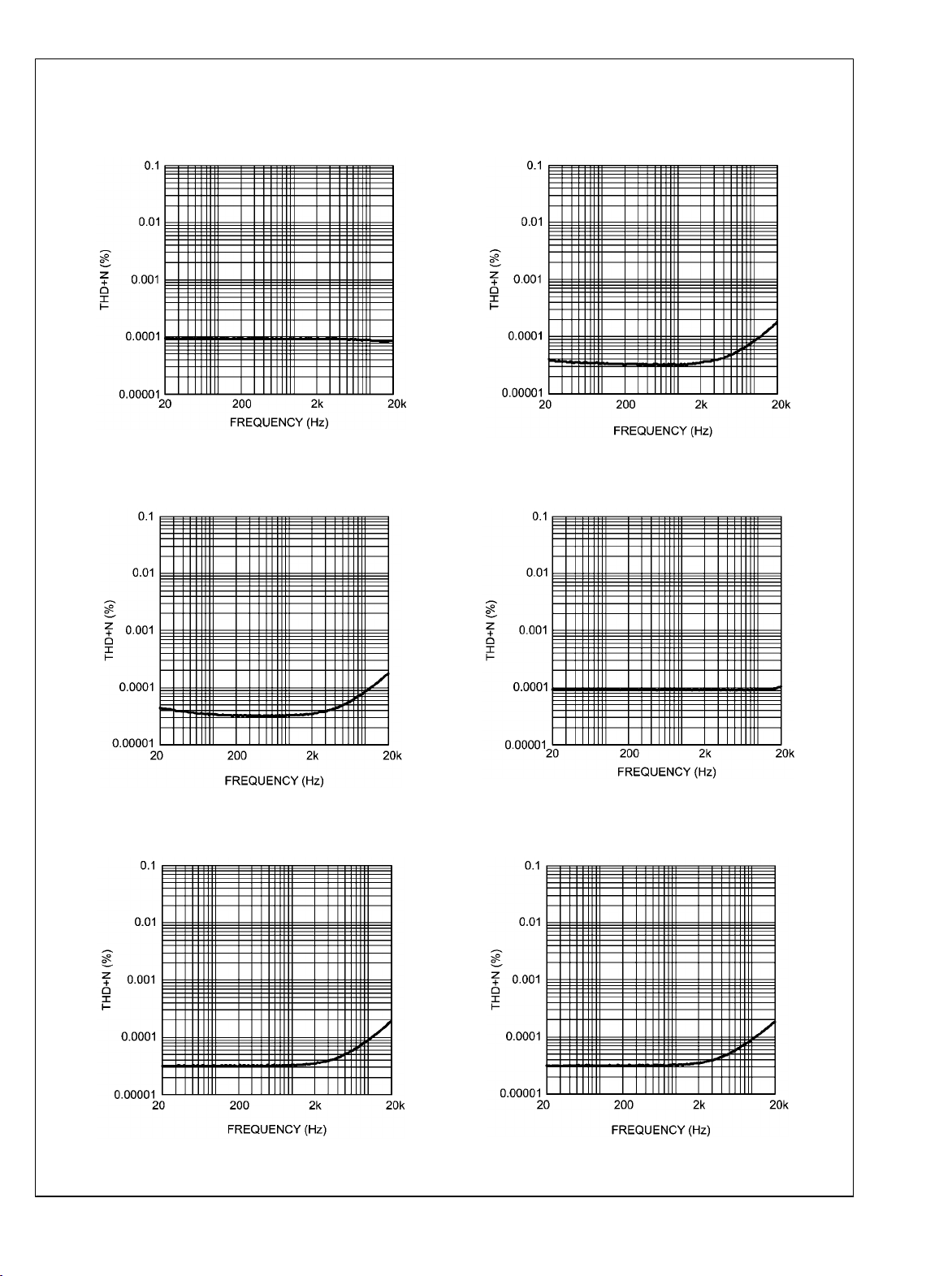
THD+N vs Frequency
VS = 4.5V, V
OUT
THD+N vs Frequency
VS = 18V, V
OUT
= 1.2V
= 3V
, RL = 600Ω
RMS
, RL = 600Ω
RMS
300342a6
THD+N vs Frequency
VS = 15V, V
OUT
THD+N vs Frequency
VS = 4.5V, V
OUT
= 3V
= 1.2V
, RL = 600Ω
RMS
, RL = 2kΩ
RMS
300342b1
THD+N vs Frequency
VS = 15V, V
OUT
= 3V
, RL = 2kΩ
RMS
300342b4
300342a9
300342a4
THD+N vs Frequency
VS = 18V, V
5 www.national.com
OUT
= 3V
, RL = 2kΩ
RMS
300342b2
LME49725
THD+N vs Frequency
VS = 4.5V, V
OUT
= 1.2V
, RL = 10kΩ
RMS
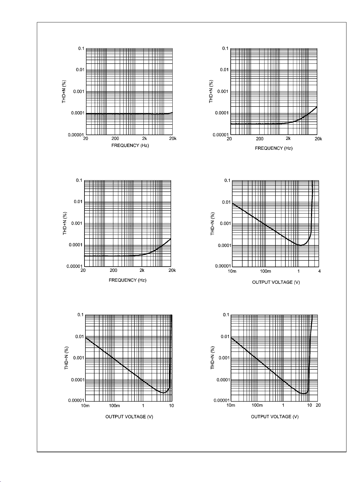
THD+N vs Frequency
VS = 15V, V
OUT
= 3V
, RL = 10kΩ
RMS
THD+N vs Frequency
VS = 18V, V
OUT
= 3V
, RL = 10kΩ
RMS
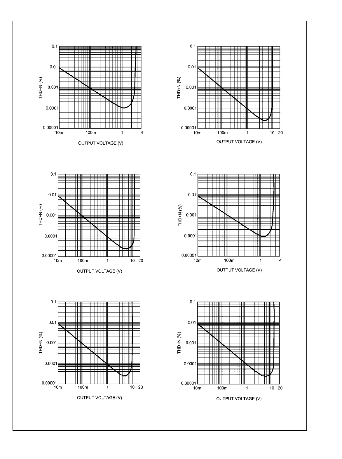
THD+N vs Output Voltage
VS = 15V, RL = 600Ω, f = 1kHz
300342a5
300342b3
300342b0
THD+N vs Output Voltage
VS = 4.5V, RL = 600Ω, f = 1kHz
30034234
THD+N vs Output Voltage
VS = 18V, RL = 600Ω, f = 1kHz
30034235
www.national.com 6
30034236
LME49725
THD+N vs Output Voltage
VS = 4.5V, RL = 2kΩ, f = 1kHz
THD+N vs Output Voltage
VS = 18V, RL = 2kΩ, f = 1kHz
30034228
THD+N vs Output Voltage
VS = 15V, RL = 2kΩ, f = 1kHz
30034229
THD+N vs Output Voltage
VS = 4.5V, RL = 10kΩ, f = 1kHz
THD+N vs Output Voltage
VS = 15V, RL = 10kΩ, f = 1kHz
30034230
30034232
30034231
THD+N vs Output Voltage
VS = 18V, RL = 10kΩ, f = 1kHz
30034233
7 www.national.com

LME49725
CMRR vs Frequency
VS = 4.5V, RL = 600Ω
CMRR vs Frequency
VS = 15V, RL = 600Ω
CMRR vs Frequency
VS = 15V, RL = 600Ω
CMRR vs Frequency
VS = 15V, RL = 2kΩ
30034283
30034285
30034284
CMRR vs Frequency
VS = 4.5V, RL = 2kΩ
30034277
CMRR vs Frequency
VS = 18V, RL = 2kΩ
30034278
www.national.com 8
30034279

LME49725
CMRR vs Frequency
VS = 4.5V, RL = 10kΩ
CMRR vs Frequency
VS = 18V, RL = 10kΩ
30034280
CMRR vs Frequency
VS = 15V, RL = 10kΩ
+PSRR vs Frequency
VS = 4.5V, RL = 2kΩ, V
RIPPLE
= 200mV
30034281
P-P
VS = 4.5V, RL = 10kΩ, V
+PSRR vs Frequency
RIPPLE
= 200mV
30034282
P-P
30034269
30034268
+PSRR vs Frequency
VS = 4.5V, RL = 600Ω, V
9 www.national.com
RIPPLE
= 200mV
P-P
30034270

LME49725
VS = 15V, RL = 2kΩ, V
+PSRR vs Frequency
RIPPLE
= 200mV
P-P
VS = 15V, RL = 10kΩ, V
+PSRR vs Frequency
RIPPLE
= 200mV
P-P
VS = 15V, RL = 600Ω, V
+PSRR vs Frequency
+PSRR vs Frequency
VS = 18V, RL = 10kΩ, V
RIPPLE
RIPPLE
= 200mV
= 200mV
30034271
P-P
30034273
P-P
VS = 18V, RL = 2kΩ, V
+PSRR vs Frequency
+PSRR vs Frequency
VS = 18V, RL = 600Ω, V
RIPPLE
RIPPLE
= 200mV
= 200mV
30034272
P-P
300342a7
P-P
30034275
www.national.com 10
30034276

LME49725
VS = 4.5V, RL = 2kΩ, V
-PSRR vs Frequency
-PSRR vs Frequency
VS = 4.5V, RL = 600Ω, V
RIPPLE
RIPPLE
= 200mV
= 200mV
P-P
30034295
P-P
VS = 4.5V, RL = 10kΩ, V
-PSRR vs Frequency
-PSRR vs Frequency
VS = 15V, RL = 2kΩ, V
RIPPLE
RIPPLE
= 200mV
= 200mV
P-P
30034296
P-P
VS = 15V, RL = 10kΩ, V
-PSRR vs Frequency
RIPPLE
= 200mV
30034297
P-P
30034299
30034298
-PSRR vs Frequency
VS = 15V, RL = 600Ω, V
11 www.national.com
RIPPLE
= 200mV
P-P
300342a0

LME49725
VS = 18V, RL = 2kΩ, V
-PSRR vs Frequency
RIPPLE
= 200mV
P-P
VS = 18V, RL = 10kΩ, V
-PSRR vs Frequency
RIPPLE
= 200mV
P-P
VS = 18V, RL = 600Ω, V
-PSRR vs Frequency
Crosstalk vs Frequency
VS = 15V, V
OUT
= 3V
= 200mV
RIPPLE
, RL = 600Ω
RMS
300342a1
P-P
300342a3
Crosstalk vs Frequency
VS = 4.5V, V
OUT
= 1.2V
Crosstalk vs Frequency
VS = 18V, V
OUT
= 3V
, RL = 600Ω
RMS
, RL = 600Ω
RMS
300342a2
30034292
30034293
www.national.com 12
30034294

LME49725
Crosstalk vs Frequency
VS = 4.5V, V
OUT
= 1.2V
Crosstalk vs Frequency
VS = 18V, V
OUT
= 3V
RMS,
, RL = 2kΩ
RMS,
, RL = 2kΩ
30034286
CrosstalkR vs Frequency
VS = 15V, V
OUT
= 3V
Crosstalk vs Frequency
VS = 4.5V, V
OUT
= 1.2V
, RL = 2kΩ
RMS,
, RL = 10kΩ
RMS,
30034287
Crosstalk vs Frequency
VS = 4.5V, V
OUT
= 1.2V
, RL = 600Ω
RMS,
30034288
30034292
30034289
Crosstalk vs Frequency
VS = 15V, V
13 www.national.com
OUT
= 3V
, RL = 10kΩ
RMS,
30034290

LME49725
Crosstalk vs Frequency
VS = 15V, V
OUT
= 3V
, RL = 600Ω
RMS,
Crosstalk vs Frequency
VS = 18V, V
OUT
= 3V
, RL = 10kΩ
RMS
Crosstalk vs Frequency
VS = 18V, V
OUT
= 3V
IMD vs Output Voltage
VS = 15V, RL = 600Ω
, RL = 600Ω
RMS
30034293
30034294
30034291
IMD vs Output Voltage
VS = 4.5V, RL = 600Ω
30034216
IMD vs Output Voltage
VS = 18V, RL = 600Ω
30034266
www.national.com 14
30034267

LME49725
IMD vs Output Voltage
VS = 4.5V, RL = 2kΩ
IMD vs Output Voltage
VS = 18V, RL = 2kΩ
30034210
IMD vs Output Voltage
VS = 15V, RL = 2kΩ
30034264
IMD vs Output Voltage
VS = 4.5V, RL = 10kΩ
IMD vs Output Voltage
VS = 15V, RL = 10kΩ
30034212
30034265
30034213
IMD vs Output Voltage
VS = 18V, RL = 10kΩ
30034215
15 www.national.com

LME49725
Total Quiescent Current vs Power Supply
30034246
Current Noise vs Frequency
VCC = 15V, VEE = –15V, No Load
Voltage Noise Density vs Frequency
VCC = 15V, VEE = –15V, No Load
30034247
300342a8
www.national.com 16

LME49725
Application Information
OPERATING RATINGS AND BASIC DESIGN GUIDELINES
The LME49725 has a supply voltage range from +9V to +36V
single supply or ±4.5V to ±18V dual supply.
Bypass capacitors for the supplies should be placed as close
to the amplifier as possible. This will help minimize any in-
ductance between the power supply and the supply pins. In
addition to a 10μF capacitor, a 0.1μF capacitor is also recommended.
The amplifier’s inputs lead lengths should also be as short as
possible. If the op amp does not have a bypass capacitor, it
may oscillate.
17 www.national.com

Demonstration Board Schematic
LME49725
30034260
www.national.com 18

Bill Of Materials For Demonstration Board (Inverting Configuration)
Description Designator Part Number Mfg
Ceramic Capacitor 0.1μF, 10% 50V
0805 SMD
Tantalum Capacitor 10μF, 10% 20V,
B-size
Resistor 0Ω, 1/8W, 1% 0805 SMD
Resistor 10kΩ, 1/8W, 1% 0805 SMD
Header, 2-Pin JP1, JP2, JP3, JP4
Header, 3-Pin JP5
SMA stand-up connectors P1-P4 (Optional) 132134 Amphenol COnnex
Note: Do not stuff Jmpr2, Jmpr3, Jmpr5, and Jmpr6.
JMPR1, JMPR4, R1, R4, R6, R9 CRCW0805000020EA Vishay
C1, C2 C0805C104K3RAC7533 Kemet
C3, C4 T491B106K025AT Kemet
R2, R3, R8, R7 CRCW080510K0FKEA Vishay
LME49725
19 www.national.com

Demonstration Board Layout
LME49725
Silkscreen Layer
Top Layer
30034262
30034263
Bottom Layer
www.national.com 20
30034261

Revision History
Rev Date Description
1.0 04/03/08 Initial release.
LME49725
21 www.national.com

Physical Dimensions inches (millimeters) unless otherwise noted
LME49725
Narrow SOIC Package
Order Number LME49725MA
NS Package Number M08A
www.national.com 22

Notes
LME49725
23 www.national.com

Notes
For more National Semiconductor product information and proven design tools, visit the following Web sites at:
Products Design Support
Amplifiers www.national.com/amplifiers WEBENCH www.national.com/webench
Audio www.national.com/audio Analog University www.national.com/AU
Clock Conditioners www.national.com/timing App Notes www.national.com/appnotes
Data Converters www.national.com/adc Distributors www.national.com/contacts
Displays www.national.com/displays Green Compliance www.national.com/quality/green
Ethernet www.national.com/ethernet Packaging www.national.com/packaging
Interface www.national.com/interface Quality and Reliability www.national.com/quality
LVDS www.national.com/lvds Reference Designs www.national.com/refdesigns
Power Management www.national.com/power Feedback www.national.com/feedback
Switching Regulators www.national.com/switchers
LDOs www.national.com/ldo
LED Lighting www.national.com/led
PowerWise www.national.com/powerwise
Serial Digital Interface (SDI) www.national.com/sdi
Temperature Sensors www.national.com/tempsensors
Wireless (PLL/VCO) www.national.com/wireless
THE CONTENTS OF THIS DOCUMENT ARE PROVIDED IN CONNECTION WITH NATIONAL SEMICONDUCTOR CORPORATION
(“NATIONAL”) PRODUCTS. NATIONAL MAKES NO REPRESENTATIONS OR WARRANTIES WITH RESPECT TO THE ACCURACY
OR COMPLETENESS OF THE CONTENTS OF THIS PUBLICATION AND RESERVES THE RIGHT TO MAKE CHANGES TO
SPECIFICATIONS AND PRODUCT DESCRIPTIONS AT ANY TIME WITHOUT NOTICE. NO LICENSE, WHETHER EXPRESS,
IMPLIED, ARISING BY ESTOPPEL OR OTHERWISE, TO ANY INTELLECTUAL PROPERTY RIGHTS IS GRANTED BY THIS
DOCUMENT.
TESTING AND OTHER QUALITY CONTROLS ARE USED TO THE EXTENT NATIONAL DEEMS NECESSARY TO SUPPORT
NATIONAL’S PRODUCT WARRANTY. EXCEPT WHERE MANDATED BY GOVERNMENT REQUIREMENTS, TESTING OF ALL
PARAMETERS OF EACH PRODUCT IS NOT NECESSARILY PERFORMED. NATIONAL ASSUMES NO LIABILITY FOR
APPLICATIONS ASSISTANCE OR BUYER PRODUCT DESIGN. BUYERS ARE RESPONSIBLE FOR THEIR PRODUCTS AND
APPLICATIONS USING NATIONAL COMPONENTS. PRIOR TO USING OR DISTRIBUTING ANY PRODUCTS THAT INCLUDE
NATIONAL COMPONENTS, BUYERS SHOULD PROVIDE ADEQUATE DESIGN, TESTING AND OPERATING SAFEGUARDS.
EXCEPT AS PROVIDED IN NATIONAL’S TERMS AND CONDITIONS OF SALE FOR SUCH PRODUCTS, NATIONAL ASSUMES NO
LIABILITY WHATSOEVER, AND NATIONAL DISCLAIMS ANY EXPRESS OR IMPLIED WARRANTY RELATING TO THE SALE
AND/OR USE OF NATIONAL PRODUCTS INCLUDING LIABILITY OR WARRANTIES RELATING TO FITNESS FOR A PARTICULAR
PURPOSE, MERCHANTABILITY, OR INFRINGEMENT OF ANY PATENT, COPYRIGHT OR OTHER INTELLECTUAL PROPERTY
RIGHT.
LIFE SUPPORT POLICY
NATIONAL’S PRODUCTS ARE NOT AUTHORIZED FOR USE AS CRITICAL COMPONENTS IN LIFE SUPPORT DEVICES OR
SYSTEMS WITHOUT THE EXPRESS PRIOR WRITTEN APPROVAL OF THE CHIEF EXECUTIVE OFFICER AND GENERAL
COUNSEL OF NATIONAL SEMICONDUCTOR CORPORATION. As used herein:
Life support devices or systems are devices which (a) are intended for surgical implant into the body, or (b) support or sustain life and
whose failure to perform when properly used in accordance with instructions for use provided in the labeling can be reasonably expected
to result in a significant injury to the user. A critical component is any component in a life support device or system whose failure to perform
can be reasonably expected to cause the failure of the life support device or system or to affect its safety or effectiveness.
National Semiconductor and the National Semiconductor logo are registered trademarks of National Semiconductor Corporation. All other
brand or product names may be trademarks or registered trademarks of their respective holders.
Copyright© 2008 National Semiconductor Corporation
For the most current product information visit us at www.national.com
National Semiconductor
LME49725 PowerWise® Dual High Performance, High Fidelity Audio Operational Amplifier
www.national.com
Americas Technical
Support Center
Email:
new.feedback@nsc.com
Tel: 1-800-272-9959
National Semiconductor Europe
Technical Support Center
Email: europe.support@nsc.com
German Tel: +49 (0) 180 5010 771
English Tel: +44 (0) 870 850 4288
National Semiconductor Asia
Pacific Technical Support Center
Email: ap.support@nsc.com
National Semiconductor Japan
Technical Support Center
Email: jpn.feedback@nsc.com
 Loading...