

LMD18400
Quad High Side Driver
LMD18400 Quad High Side Driver
June 1996
General Description
The LMD18400 is a fully protected quad high side driver. It
contains four common-drain DMOS N-channel power
switches, each capable of switching a continuous 1 Amp
>
3 Amps transient) to a common positive power sup-
load (
ply. The switches are fully protected from excessive voltage,
current and temperature. An instantaneous power sensing
circuit calculates the product of the voltage across and the
current through each DMOS switch and limits the power to a
safe level. The device can be disabled to produce a “sleep”
condition reducing the supply current to less than 10 µA.
Separate ON/OFF control of each switch is provided through
standard LSTLL/CMOS logic compatible inputs.
™
A MICROWIRE
to provide extensive diagnostic information. This information
includes switch status readback, output load fault conditions
and thermal and overvoltage shutdown status. There are
also two direct-output error flags to provide an immediate
indication of a general system fault and an indication of
excessive operating temperature.
The LMD18400 is packaged in a special power dissipating
leadframe that reduces the junction to case thermal resistance to approximately 20˚C/W.
compatible serial data interface is built in
Features
n Four independent outputs with>3A peak, 1A continuous
current capability
n 1.3Ω maximum ON resistance over temperature
n True instantaneous power limit for each switch
n High survival voltage (60 V
n Shorted load (to ground and supply) protection
n Overvoltage shutdown at V
n LS TTL/CMOS compatible logic inputs and outputs
<
n
10 µA supply current in “sleep” mode
n −5V output clamp for discharging inductive loads
n Serial data interface for 11 diagnostic checks:
— Switch ON/OFF status
— Open or shorted load
— Operating temperature
— Excessive supply voltage
n Two direct-output error flags
, 80V transient)
DC
>
35V
CC
Applications
n Relay and solenoid drivers
n High impedance automotive fuel injector drivers
n Lamp drivers
n Power supply switching
n Motor drivers
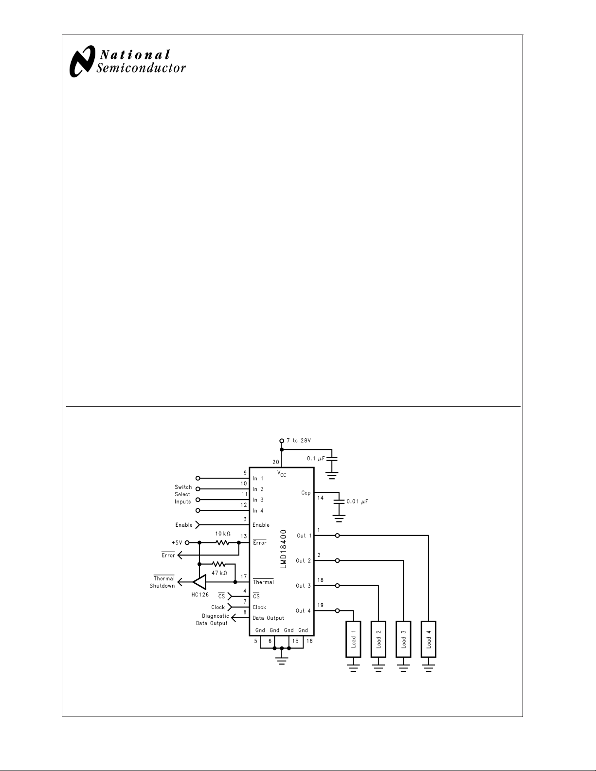
Typical Application
01102601
© 2004 National Semiconductor Corporation DS011026 www.national.com
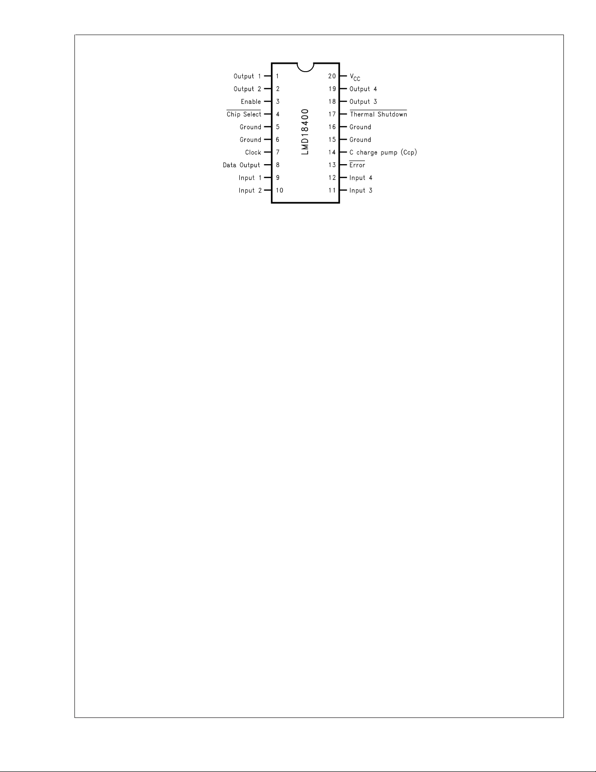
Connection Diagram
LMD18400
Order Number LMD18400N
See NS Package Number N20A
01102602
www.national.com 2
LMD18400
Absolute Maximum Ratings (Note 1)
If Military/Aerospace specified devices are required,
please contact the National Semiconductor Sales Office/
Distributors for availability and specifications.
Supply Survival Voltage (Pin 20)
Transient (t = 10 ms) 80V
Continuous −0.5V to +60V
Output Transient Current (Each Switch) 3.75A
Logic Input Voltage (Pins 4, 7) −0.3V to +6V
Error Flag Voltage 16V
ESD Susceptibility (Note 2) 2000V
Power Dissipation (Note 3) 5W
Internally Limited
Junction Temperature (T
150˚C) 150˚C
J
MAX
Storage Temperature Range −65˚C to +150˚C
Lead Temperature (Soldering, 10 sec.) +260˚C
Output Transient Current
(Total, All Switches) 6A
Operating Ratings (Note 1)
Output Steady State Current
(Each Switch) 1A
Logic Input Voltage
Ambient Temperature Range (T
Supply Voltage Range 7V to 28V
) −25˚C to +85˚C
A
(Pins 3, 9, 10, 11, 12) −0.3V to +16V
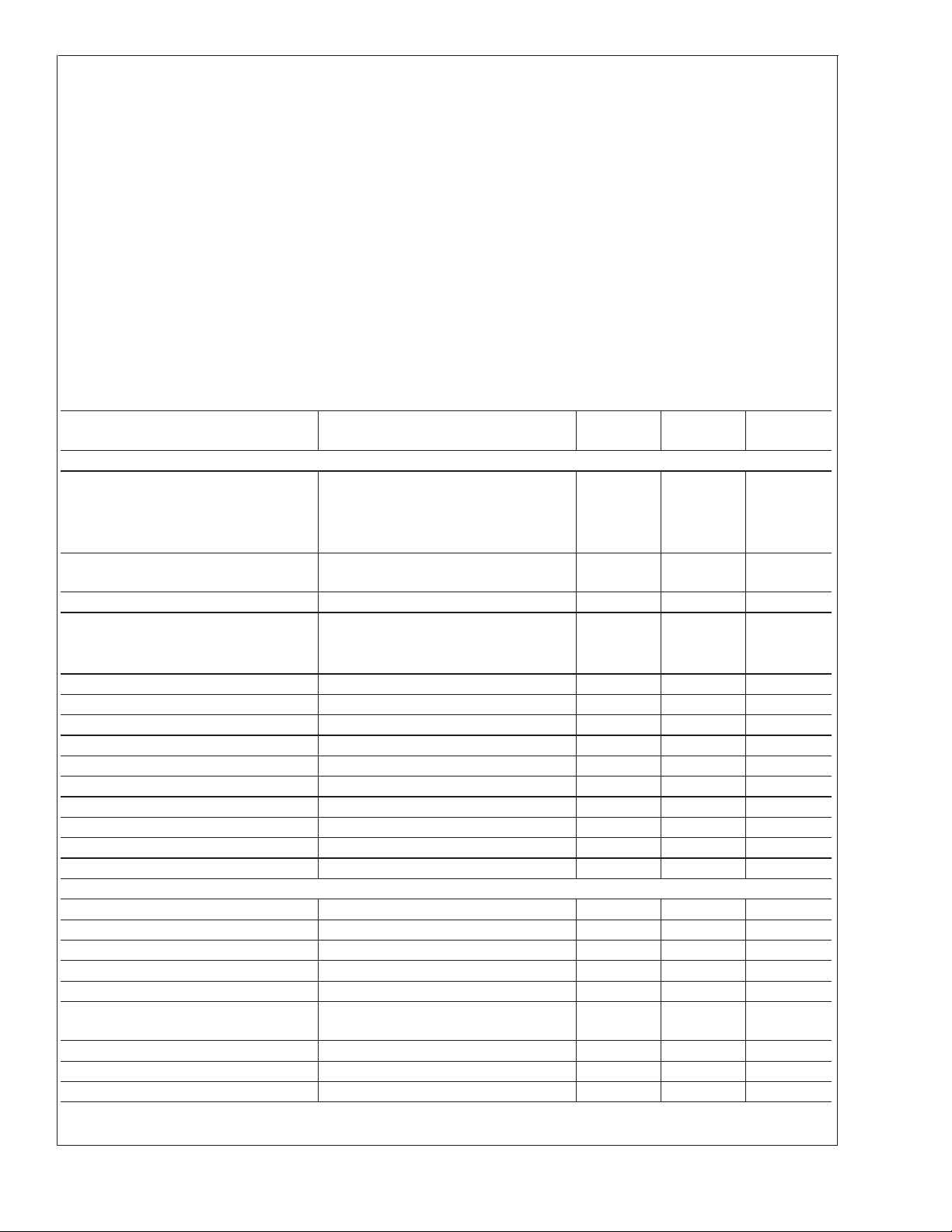
Electrical Characteristics V
over the entire operating temperature range, −25˚C ≤ T
Parameter Conditions
= 12V, CCP= 0.01 µFd, unless otherwise indicated. Boldface limits apply
CC
≤ +85˚C, all other limits are for TA=TJ= +25˚C.
A
Typical
(Note 4)
Limit
(Note 5)
Units
(Limit)
DC CHARACTERISTICS
Supply Current Enable Input = 0V 0.04 10 µA (Max)
Enable Input = 5V, Inputs = 0V 7.5 15 mA (Max)
Enable Input = 5V, Inputs = 5V
Open Loads 7.5 15 mA (Max)
Output Leakage Enable Input = 0V, Inputs = 0V
(Pins 1, 2, 18, 19)
Rds ON I
Short Circuit Current V
Maximum Output Current V
= 1A, (Note 6) 0.8 1.3 Ω (Max)
OUT
= 12V, (Note 6) 1.2 0.6 A (Min)
CC
V
= 7V, (Note 6) 2.4 A
CC
V
= 28V, (Note 6) 0.6 A
CC
CC−VO
= 4V, (Note 6) 3.75 A
0.01 300 µA (Max)
Lead Error Threshold Voltage Pins 1, 2, 18, 19 4.1 V
Open Load Detection Current Pins 1, 2, 18, 19 150 µA
Negative Clamp Output Voltage I
= 1A, (Note 6) −5 V
O
Overvoltage Shutdown Threshold 31 40 V (Max)
Overvoltage Shutdown Hysteresis 0.75 V
Error Output Leakage Current V
Thermal Warning Temperature V
Thermal Shutdown Temperature V
Thermal Warning Temperature V
= 12V 0.001 10 µA (Max)
PIN 13
<
PIN 13
PIN 17
PIN 13
0.8V 145 ˚C
<
0.8V 170 ˚C
<
0.8V 145 ˚C
AC CHARACTERISTICS
Switch Turn-On Delay (t
Switch Turn-On Rise Time (t
Switch Turn-Off Delay (t
Switch Turn-Off Fall Time (t
Enable Time (t
) Measured with Switch 1, Pin9=5V 30 50 µs(Max)
EN
Error Reporting Delay (t
Data Setup Time (t
TRI-STATE
DS
®
Control (t1H,tOH) Pin 8, Hi-Z Enable Time 2 µs
) Enable (Pin 3) = 5V, I
d(ON)
)I
ON
) Enable (Pin 3) = 5V, I
d(OFF)
)I
OFF
) Enable (Pin 3) = 5V, Switch 1 Load
Error
= 1A 7 15 µs (Max)
OUT
= 1A 0.15 1 µs (Max)
OUT
Opened
)C
= 30 pF 200 500 ns (Min)
L
= 1A 5 10 µs (Max)
OUT
= 1A 0.5 2 µs (Max)
OUT
75 150 µs (Max)
Data Clock Frequency 3 1 MHz (Max)
www.national.com3
Electrical Characteristics V
= 12V, CCP= 0.01 µFd, unless otherwise indicated. Boldface limits apply over
CC
the entire operating temperature range, −25˚C ≤ T
≤ +85˚C, all other limits are for TA=TJ= +25˚C. (Continued)
A
LMD18400
Parameter Conditions
Typical
(Note 4)
Limit
(Note 5)
DIGITAL CHARACTERISTICS
Logic “1” Input Voltage Pins 3, 4, 7, 9, 10, 11, 12 2.0 V (Min)
Logic “0” Input Voltage Pins 3, 4, 7, 9, 10, 11, 12 0.8 V (Max)
Logic “1” Input Current Pins 4, 7 0.001 1 µA (Max)
Logic “0” Input Current Pins 4, 7 −0.001 −1 µA (Max)
TRI-STATE Output Current Pin 8, Pin4=5V 0.05 10 µA (Max)
Pin8=0V −0.05 −10 µA (Max)
Enable Input Current Pin 3 = 2.4V 12 25 µA (Max)
Channel Input Resistance Pins 9, 10, 11, 12 75 15 kΩ (Min)
Error Output Sink Current Pin 13 = 0.8V 4 1.6 mA (Min)
Logic “1” Output Voltage Pin 8
I
= −360 µA 4.4 2.4 V (Min)
OUT
I
= −10 µA 5.1 4.5 V (Min)
OUT
I
= −10 µA 5.5 V (Min)
OUT
Logic “0” Output Voltage Pin 8
I
OUT
Thermal Shutdown Output Source
Pin 17 = 2.4V
Current
= 100 µA
5 3 µA (Min)
0.4 V (Max)
Thermal Shutdown Output Sink Current Pin 17 = 0.8V 360 250 µA (Min)
Note 1: Absolute Maximum Ratings indicate limits beyond which damage to the device may occur. Operating Ratings indicate conditions for which the device is
intended to be functional, but do not guarantee specific performance limits. For guaranteed specifications and test conditions, see the Electrical Characteristics.
Note 2: Human body model; 100 pF discharge through a 1.5 kΩ resistor. All pins except pins 8 and 13 which are protected to 1000V and pins 1, 2, 18 and 19 which
are protected to 500V.
Note 3: The maximum power dissipation is a function of T
ambient temperature is P
shutdown. For the LMD18400 the junction-to-ambient thermal resistance, θ
the package will be, I
Note 4: Typical values are at T
Note 5: All limits are 100% production tested at +25˚C. Limits at temperature extremes are guaranteed through correlation and accepted Statistical Quality Control
(SQC) methods.
Note 6: Pulse Testing techniques used. Pulse width is
=(T
D
DC
MAX
–TA)/θJA. If this dissipation is exceeded, the die temperature will rise above 150˚C and the device will eventually go into thermal
J
MAX
2
xR
J
x 4 switches 1A2x 1.3Ω x 4 = 5.2W).
ON
(MAX)
= +25˚C and represent the most likely parametric norm.
, θJA, and TAand is limited by thermal shutdown. The maximum allowable power dissipation at any
J
MAX
, is 60˚C/W. With sufficient heatsinking the maximum continuous power dissipation for
JA
<
5 ms with a duty cycle<1%.
Units
(Limit)
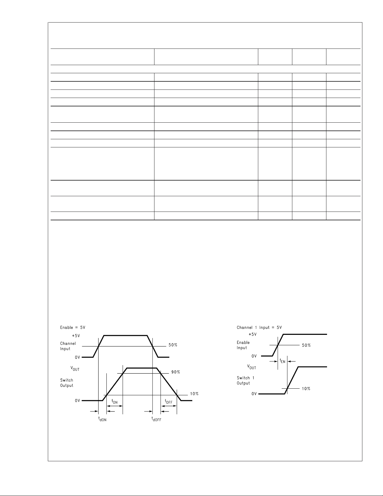
Timing Specification Definitions
Switching Turn ON/OFF Enable Turn-On
01102603
www.national.com 4
01102604
Timing Specification Definitions (Continued)
Error Reporting Delay Data Setup Time
LMD18400
01102605
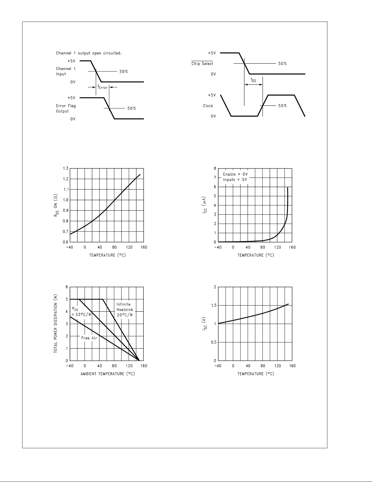
Typical Performance Characteristics For all curves, V
perature unless otherwise noted.
Switch ON Resistance
vs Temperature
01102631
Maximum Power Dissipation
vs Ambient Temperature
= 12V, Temperature is the junction tem-
CC
“Sleep Mode” Supply Current
vs Temperature
01102632
Short Circuit Current
vs Temperature
01102606
01102633
01102634
www.national.com5
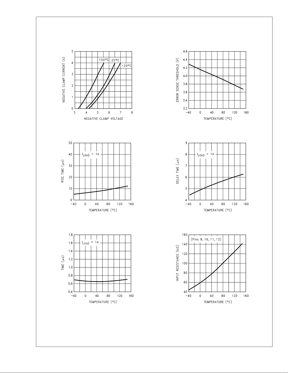
Typical Performance Characteristics For all curves, V
temperature unless otherwise noted. (Continued)
= 12V, Temperature is the junction
CC
LMD18400
Clamp Characteristics
vs Temperature
Turn ON Rise Time
vs Temperature
01102635
Error Sense Threshold
Voltage vs Temperature
01102636
Turn ON Delay Time
vs Temperature
Turn OFF Time
vs Temperature
01102637 01102638
Switch Select Logic Input
Resistance vs Temperature
01102639
01102640
www.national.com 6

LMD18400
Typical Performance Characteristics For all curves, V
temperature unless otherwise noted. (Continued)
Enable Threshold Voltage
vs Temperature
01102641 01102642
Functional Block Diagram
= 12V, Temperature is the junction
CC
Error Output Voltage
vs Sink Current
01102608
www.national.com7
Truth Table
Enable
LMD18400
Input
(Pin 3)
Chip Select
Input
(Pin 4)
Switch Control
Input
(Pins 9, 10, 11, 12)
0 X X 1 0 “Sleep” Mode, I
1 X 0 1 1 Selected Switch is OFF
1 X 1 1 1 Selected Switch is ON, Normal Operation
1 X 0 0 1 Switch is OFF but:
1 X 1 0 1 Switch is ON, but:
1X 1 0 0T
1 1 X X X Data Output Pin is TRI-STATE
1 0 X X X Data Output Pin is Enabled and Ready to
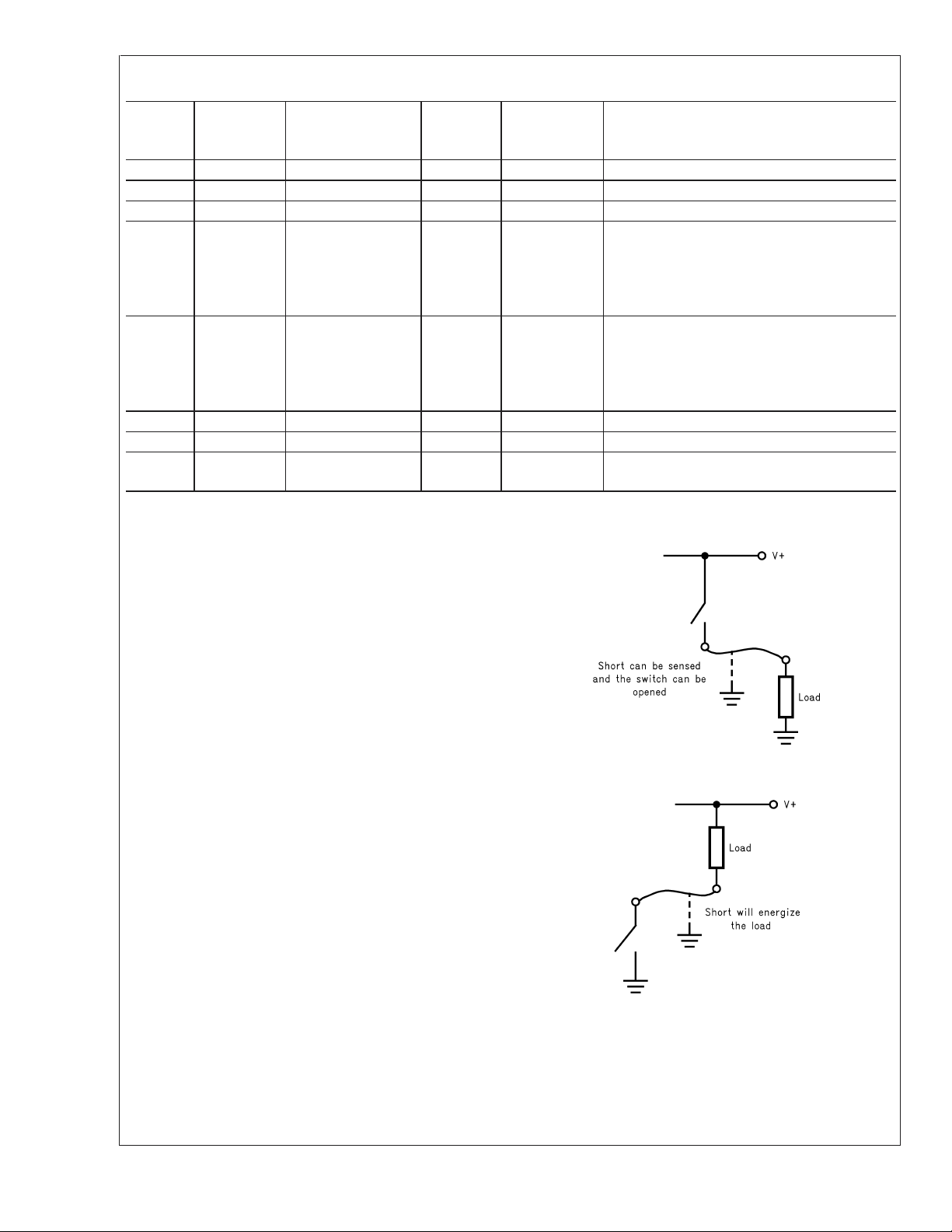
Applications Information
BASIC OPERATION
High-side drivers are used extensively in automotive and
industrial applications to switch power to ground referred
loads. The major advantage of using high-side drive, as
opposed to low-side drive, is to protect the load from being
energized in the event that the load drive wire is inadvertently shorted to ground as shown in Figure 1. A high-side
driver can sense a shorted condition and open the power
switch to disable the load and eliminate the excessive current drain on the power supply. The LMD18400 can control
and protect up to four separate ground referenced loads.
Error
Output
(Pin 13)
Thermal SD
Output
(Pin 17)
Conditions
<
SUPPLY
10 µA
a. Load is Open Circuited, or
b. Load is Shorted to V
>
c. T
d. V
+145˚C, or
J
>
CC
+35V
,or
CC
a. Load is Shorted to Ground, or
b. Switch is in Power Limit, or
>
c. T
d. V
J
+145˚C, or
J
>
+35V and Switch is Actually OFF
CC
>
+170˚C, All Switches are OFF
Output Diagnostic Information
High Side Drive
www.national.com 8
01102609
Low Side Drive
01102610
FIGURE 1. High-Side vs Low-Side Drive
The LMD18400 combines low voltage CMOS logic control
circuitry with a high voltage DMOS process. Each DMOS
power switch has an individual ON/OFF control input. When
commanded ON, the output of the switch will connect the
load to the V
supply through a maximum resistance of
CC
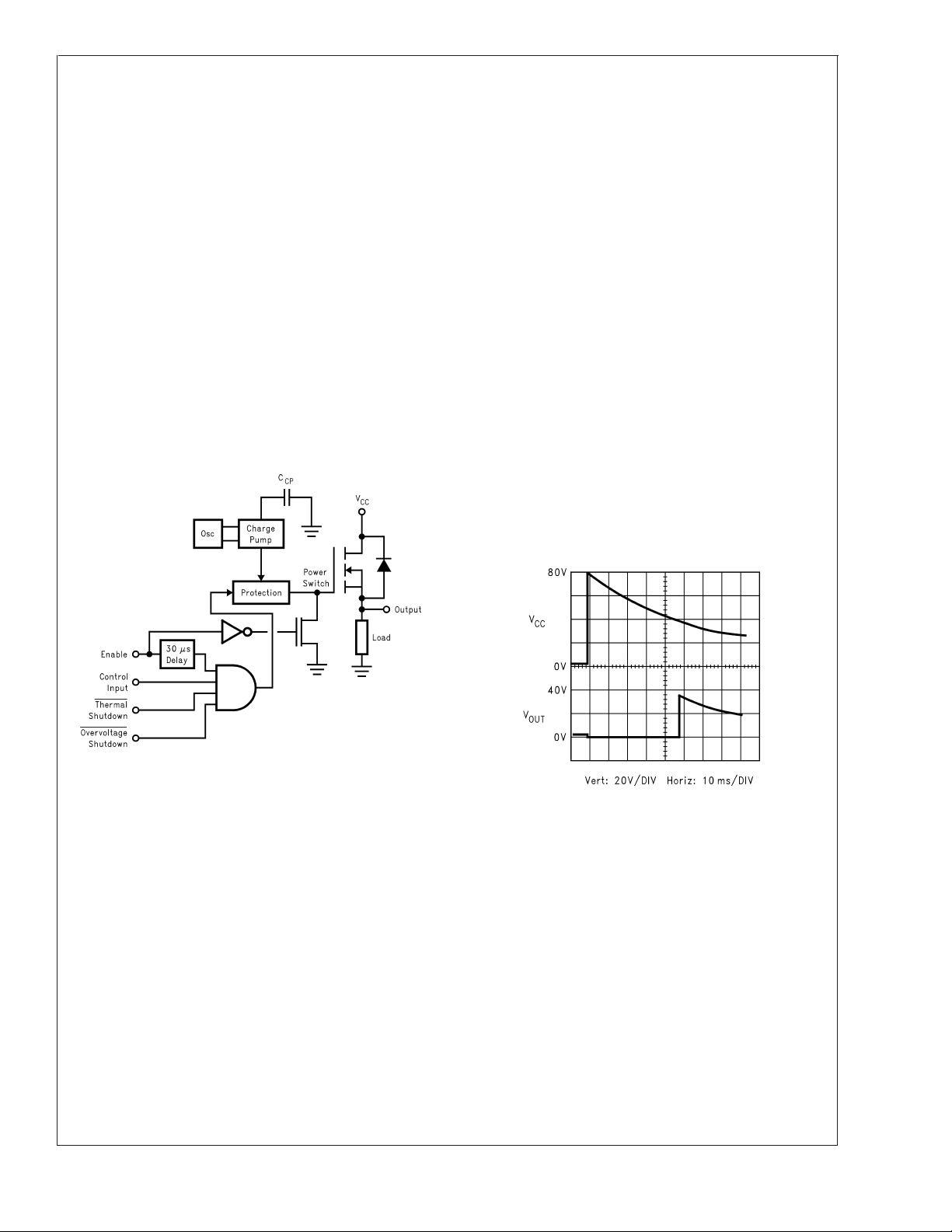
Applications Information (Continued)
1.3Ω (the ON resistance of the DMOS switch). The voltage
applied to the load will depend upon the load current and the
designed current capability of the LMD18400. When a switch
is commanded OFF, the load will be disconnected from the
supply except for a small leakage current of typically less
than 0.01 µA.
The LMD18400 can be continually connected to a live power
source, a car battery for example, while drawing less than
10 µA from the power source when put into a “sleep” condition. This “sleep” mode is enacted by taking the Enable Input
(pin 3) low. During this mode the supply current for the
device is typically only 0.04 µA. Special low current consumption standby circuitry is used to hold the DMOS
switches OFF to eliminate the possibility of supply voltage
transients from turning on any of the loads (a common
problem with MOS power devices). When in the “sleep”
mode, all diagnostic and logic circuitry is inactive. When the
Enable Input is taken to a logic 1, the switches become
“armed” and ready to respond to their control input after a
short, 30 µs, enable delay time. This delay interval prevents
the switches from transient turn-on. Figure 2 shows the
switch control logic.
PROTECTION CIRCUITRY
The LMD18400 has extensive protection circuitry built in.
With any power device, protection against excessive voltage, current and temperature conditions is essential. To
achieve a “fail-safe” system implementation, the loads are
deactivated automatically by the LMD18400 in the event of
any detected overvoltage or over-temperature fault conditions.
Voltage Protection
The V
supply can range from −0.5V to +60 VDCwithout
CC
any damage to the LMD18400. The CMOS logic circuitry is
biased from an internal 5.1V regulator which protects these
lower voltage transistors from the higher V
potentials. In
CC
order to protect the loads connected to the switch outputs
however, an overvoltage shutdown circuit is employed.
Should the V
potential exceed 35V all of the switches are
CC
turned OFF thereby disconnecting the loads. This 35V
threshold has 750 mV of hysteresis to prevent potential
oscillations.
Additionally, there is an undervoltage lockout feature built in.
With V
less than 5V it becomes uncertain whether the
CC
logic circuitry can hold the switches in their commanded
state. To avoid this uncertainty, all of the switches are turned
OFF when V
illustrates the shutoff of an output during a 0V to 80V V
drops below approximately 5V. Figure 3
CC
CC
supply transient.
LMD18400
01102611
FIGURE 2. Control Logic for Each Power Switch
Each DMOS switch is turned ON when its gate is driven
approximately 3.5V more positive than its source voltage.
Because the source of the switch is the output terminal to the
load it can be taken to a voltage very near the V
CC
supply
potential. To ensure that there is sufficient voltage available
to drive the gates of the DMOS device a charge pump circuit
is built in. This circuit is controlled by an internal 300 kHz
oscillator and using an external 10 nF capacitor connected
from pin 14 to ground generates a voltage that is approximately 20V greater than the V
supply voltage. This pro-
CC
vides sufficient gate voltage drive for each of the switches
which is applied under command of standard 5V logic input
levels.
The turn-on time for each switch is approximately 12 µs
when driving a 1A load current. This relatively slow switching
time is beneficial in minimizing electromagnetic interference
(EMI) related problems created from switching high current
levels.
Over/Under
Voltage Shutdown
01102612
FIGURE 3. Overvoltage/Undervoltage Shutdown
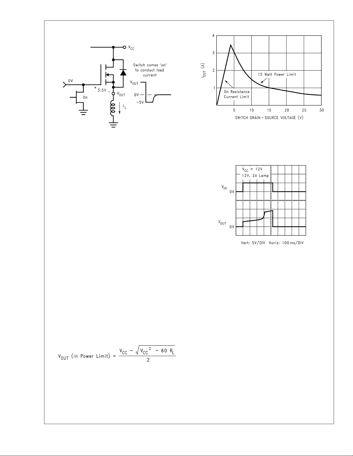
The LMD18400 has been designed to drive all types of
loads. When driving a ground referenced inductive load such
as a relay or solenoid, the voltage across the load will
reverse in polarity as the field in the inductor collapses when
the power switch is turned OFF. This will pull the output pin
of the LMD18400 below ground. This negative transient
voltage is clamped at approximately −5V to protect the IC.
This clamping action is not done with diodes but rather the
power DMOS switch turning back on momentarily to conduct
the inductor current as it de-energizes as shown in Figure 4.
www.national.com9
Applications Information (Continued)
LMD18400
FIGURE 4. Turn-OFF Conditions with an Inductive
Load
01102614
01102613
FIGURE 5. Maximum Output Current with
Instantaneous Power Limiting
When the output inductance produces a negative voltage,
the gate of the DMOS transistor is clamped at 0V. At −3.5V,
the source of the power device is less than the gate by
enough to cause the switch to turn ON again. During this
negative transient condition the power limiting circuitry to
protect the switch is disabled due to the gate being held at
0V. The maximum current during this clamping interval,
which is equal to the steady state ON current through the
inductor, should be kept less than 1A. Another concern
during this interval has to do with the size of an inductive
load and the amount of time required to de-energize it. With
larger inductors it may be possible for the additional power
dissipation to cause the die temperature to exceed the thermal shutdown limit. If this occurs all of the other switches will
turn OFF momentarily (see section on Thermal Management).
Power Limiting
The LMD18400 utilizes a true instantaneous power limit
circuit rather than simple current limiting to protect each
switch. This provides a higher transient current capability
while still maintaining a safe power dissipation level. The
power dissipation in each switch (the product of the Drainto-Source voltage and the output current, V
dsxIOUT
)is
continually monitored and limited to 15W by varying the gate
voltage and therefore the ON resistance of the switch. Basically the ON resistance will be as low as possible until 15W
is being dissipated. To maintain 15W, the ON resistance
increases to reduce the load current. This results in a decrease of the output voltage. For resistive loads, the output
voltage when in power limit will be:
This provides a maximum transient current, and drain-tosource voltage characteristic as shown in Figure 5.
Driving a Lamp
01102615
FIGURE 6. Soft Turn-On of a Lamp Load
The steady state current to the load is limited by the package
power dissipation, ambient temperature and the ON resistance of the switch which has a positive temperature coefficient as shown in the Typical Performance Characteristics.
This dynamic current limiting of the switches is beneficial
when driving lamp and large capacitive loads. Lamps require
a large inrush current, on the order of 10 times the normal
operating current, when first switched on with a cold filament. The LMD18400 will limit this initial current to the level
where 15W is dissipated in the switch. As the filament warms
up the voltage across the lamp increases thereby decreasing the voltage across the switch which permits more current
to fully light the lamp. With limited inrush current the lifetime
of a lamp load is increased significantly. Figure 6 illustrates
the soft turn-on of a lamp load.
The same principle of increasing output current as the voltage across the load increases allows large capacitive loads
to be charged more quickly by an LMD18400 driver than as
opposed to a driver with a fixed 1A current limit protection
scheme. Figure 7 shows the output response while driving a
large capacitive load.
www.national.com 10

Applications Information (Continued)
Thermal Protection
The die temperature of the LMD18400 is continually monitored. Should any conditions cause the die temperature to
rise to +170˚C, all of the power switches are turned OFF
automatically to reduce the power dissipation. It is important
to realize that the thermal shutdown affects all four of the
switches together. That is, if just one switch load is enough to
heat the die to the thermal shutdown threshold, all of the
other switches, regardless of their power dissipation conditions, will be switched OFF. All of the switches will be reenabled when the die temperature has cooled to approximately +160˚C. Until the high temperature forcing conditions
have been removed the switches will cycle ON and OFF thus
maintaining an average die temperature of +165˚C. The
LMD18400 will signal that excessive temperatures exist
through several diagnostic output signals (see Diagnostics).
Driving a Large
Capacitive Load
01102616
FIGURE 7. Driving a Large Capacitive Load
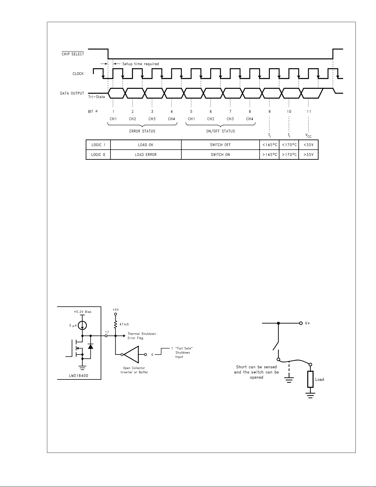
DIAGNOSTICS
The LMD18400 has extensive circuit diagnostic information
reporting capability. Use of this information can produce
systems with intelligent feedback of switch status as well as
load fault conditions for troubleshooting purposes. All of the
diagnostic information is contained in an 11-bit word. This
data can be clocked out of the LMD18400 in a serial fashion
as shown in Figure 8. The shift register is parallel loaded with
the diagnostic data whenever the Chip Select input is at a
Logic 1 and changes to the serial shift mode when Chip
Select is taken to a Logic 0. The Data Output line (pin 8) is
biased internally from a 5.1V regulator which sets the Logic
1 output voltage. This pin has low current sourcing capability
so any load on this pin will reduce the Logic 1 output level
which is guaranteed to be at least 2.4V with a 360 µA load.
The data interface is MICROWIRE compatible in that data is
clocked out of the LMD18400 on the falling edge of the clock,
to be clocked into the controlling microprocessor on the
rising edge. Any number of devices can share a common
data output line because the data output pin is held in a high
impedance (TRI-STATE) condition until the device is se-
lected by taking its Chip Select Input low. Following Chip
Select going low there is a short data setup time interval
(500 ns Min) required. This is necessary to allow the first
data bit of information to be established on the data output
line prior to the first rising clock edge which will input the data
bit into the controller. When all 11 bits of diagnostic data
have been shifted out the data output goes to a Logic 1 level
until the Chip Select line is returned high.
Figure 8 also indicates the significance of the diagnostic data
bits. The first 4 bits indicate an output load error condition,
one for each channel in succession (see Load Error Detec-
tion).
Bits 5 through 8 provide a readback of the commanded
ON/OFF status of each switch.
A unique feature of the LMD18400 is that it provides an early
warning of excessive operating temperature. Should the die
temperature exceed +145˚C, bit 9 will be set to a Logic 0.
Acting on this information a system can be programmed to
take corrective action, shutting OFF specific loads perhaps,
while the LMD18400 is still operating normally (not yet in
thermal shutdown). If this early warning is ignored and the
device continues to rise in temperature, the thermal shut-
down circuitry will come into action at a die temperature of
+170˚C. Should this occur bit 10 of the diagnostic data
stream will be set to a Logic 0 indicating that the device is in
thermal shutdown and all of the outputs have been shut OFF.
The final data bit, bit 11, indicates an overvoltage condition
on the V
indicates that all of the drivers are OFF.
The diagnostic data can be read periodically by a controller
or only in the event of a general system error indication to
determine the cause of any system problem. This general
indication of a fault is provided by an Error Flag output (pin
13). This pin goes low whenever any type of error is de-
tected. There is a built-in delay of approximately 75 µs from
the time an error is detected until pin 13 is taken low. This is
to help mask short duration error conditions such as may be
caused by driving highly capacitive loads (
load may generate a shorted load error for several hundred
milliseconds as it turns on which should be ignored.
supply (VCCis greater than 35V) and again
CC
>
2 µF). A lamp
LMD18400
www.national.com11
Applications Information (Continued)
LMD18400
FIGURE 8. Serial Diagnostic Data Assignments
01102617
The Error Flag output pin is an open drain transistor which
requires a pull-up resistor to a positive voltage of up to 16V.
Typically this pull-up is to the same 5V supply which is
biasing the Enable input and any other external logic circuitry. The Error Flag pins of several LMD18400 packages
can be connected together with just one pull-up resistor to
provide an all-encompassing general system error indication. Upon detection of an error, each device could then be
polled for diagnostic information to determine the source of
the fault condition.
A second direct output error flag is for an indication of
Thermal Shutdown (pin 17). This active low flag provides an
immediate indication that the die temperature has reached
+170˚C and that the drive to all four switches has been
removed. This output is pulled up to the internal 5.1V logic
regulator through a small (5 µA) current source so use of a
buffer on this pin is recommended.
under any sort of externally detected system fault condition.
The diagnostic logic however does not distinguish between
normal thermal shutdown or the fact that pin 17 has been
driven low. As such, various switch errors and an overtemperature indication will be reported in the diagnostic data
stream.
Figure 9 illustrates the use of pin 17 as both an output
thermal shutdown flag and as an input to shut down only the
switches. Directly tying pin 17 to +5V will prevent the internal
thermal shutdown circuitry from disabling the switches. For
reliability purposes however this is not recommended as
there will then be no limit to the maximum die temperature.
Refer to the Truth Table for a summary of the action of these
direct-output error flags.
LOAD ERROR DETECTION
An important feature of the LMD18400 is the ability to detect
open or shorted load connections. Figure 10 illustrates the
detection circuit used with each of the drivers.
01102618
FIGURE 9. Thermal Shutdown Flag and Shutdown
Input
A useful feature of pin 17 is that it can also be used as a
shutdown input. Driving this pin low immediately switches all
of the drivers OFF, just the same as if thermal shutdown
temperatures has been reached, yet all of the control logic
and diagnostic circuits remain active. This is useful in designing “fail-safe” systems where the loads can be disabled
www.national.com 12
01102609
FIGURE 10. Detection Circuitry for Open/Shorted
Loads
A voltage comparator monitors the voltage to the load and
compares it to a fixed 4.1V reference level. When a switch is
OFF, the ground referenced load should have no voltage
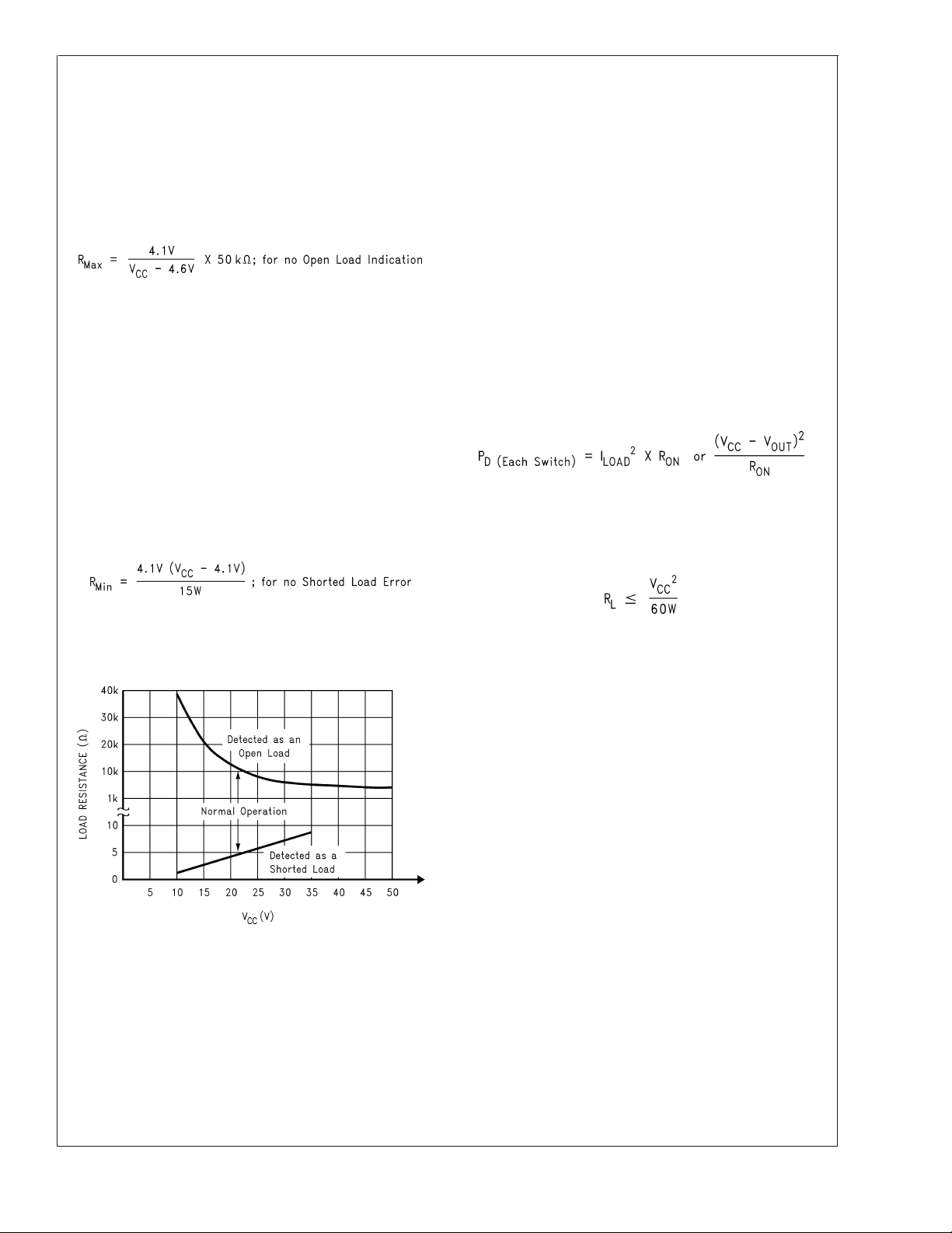
LMD18400
Applications Information (Continued)
across it. Under this condition, an internal 50 kΩ resistor
connected to V
the load. If the load resistance is large enough to create a
voltage greater than 4.1V an Open Load Error will be indicated for that switch. The maximum load resistance that will
not generate an Open Load Error when a switch is OFF can
be found by:
To make this Open Load Error threshold more sensible, an
external pull-up resistor can be added from the output to the
supply.
V
CC
Also when a switch is commanded OFF, should the load be
shorted to the V
indicate an error.
When a switch is commanded ON, the load is expected to
have a voltage across it that approaches the V
the output voltage is less than the 4.1V threshold an error will
again be reported, indicating that the load is either shorted to
ground or that the driver is in power limit and not able to pull
the output voltage any closer to V
resistance that will not generate a Shorted Load Error when
a switch is ON can be found by:
will provide a small amount of current to
CC
supply, this same circuitry will again
CC
potential. If
CC
. The minimum load
CC
THERMAL MANAGEMENT
It is particularly important to consider the total amount of
power being dissipated by all four switches in the LMD18400
at all times. Any combination of the switches driving loads
will cause an increase in the die temperature. Should the die
temperature reach the thermal shutdown threshold of
+170˚C, all of the switches will be disabled.
Careful calculation of the worst case total power dissipation
required at any point in time, together with providing suffi-
cient heatsinking will prevent this from occurring.
The LMD18400 is packaged with a special leadframe that
helps dissipate heat through the two ground pins on each
side of the package. The thermal resistance from junction-
to-case (θ
thermal resistance from junction-to-ambient (θ
) for this package is approximately 20˚C/W. The
JC
), without
JA
any heatsinking, is approximately 60˚C/W. Figure 12 illus-
trates how the copper foil of a printed circuit board can be
designed to provide heatsinking and reduce the overall
junction-to-ambient thermal resistance.
The power dissipation in each switch is equal to:
where RONis the ON resistance of the switch (1.3Ω maxi-
mum). These equations hold true until the power dissipation
reaches the maximum limit of 15W. With resistive loads, the
15W power limit threshold will be reached when:
Figure 11 indicates the range of load resistance for normal
operation, open load, and shorted load or power limit indication.
01102620
FIGURE 11. Load Resistance Detected as Errors
Inductive loads will create additional power dissipation when
switched OFF. Figure 13 shows the idealized voltage and
current waveforms for an inductive load.
www.national.com13

Applications Information (Continued)
LMD18400
Maximum Power Dissipated
and Junction to Ambient
Thermal Resistance vs Size
01102622
01102621
FIGURE 12. Recommended PC Board Layout to Reduce the Thermal Resistance from Junction-to-Ambient
for the time interval, t
. which is the time required for the
CLAMP
inductor current to fall to zero:
01102623
FIGURE 13. Switching an Inductive Load
When switched ON, the worst case power dissipation is:
The steady-state ON current of the inductor should be kept
less than 1A per power switch.
The additional power dissipation during turn-off, as the inductor is de-energized and the voltage across the inductor is
clamped to −5V, can be found by:
The size of the inductor will determine the time duration for
this additional power dissipation interval. Even though the
peak current is kept less than 1A, the switch during this
interval will see a voltage across it of V
+ 5V with no power
CC
limit protection. If the inductor is too large, the time interval
may be long enough to heat the die temperature to +170˚C
thereby shutting OFF all other loads on the package.
The total average power dissipation during a full ON/OFF
switching cycle of an inductive load will be:
Due to the common cut-off of all loads forced by thermal
shutdown, the thermal time constants of the package become a concern. Figure 14 provides an indication of the time
it takes to heat the die to thermal shutdown with a step
increase in package power dissipation from an initial junction
temperature of +25˚C. This data was measured using a PC
board layout providing a thermal resistance from junction to
ambient of approximately 35˚C/W. Less heatsinking will, of
course, result in faster thermal shutdown of the power
switches.
www.national.com 14

Applications Information (Continued)
01102624
FIGURE 14. Approximate time required for the die to reach the 170˚C thermal shutdown point from 25˚C for different
total package power dissipation levels.
ON/OFF Switching of Multiple Voltage Regulated Circuit Loads
LMD18400
www.national.com15
01102625
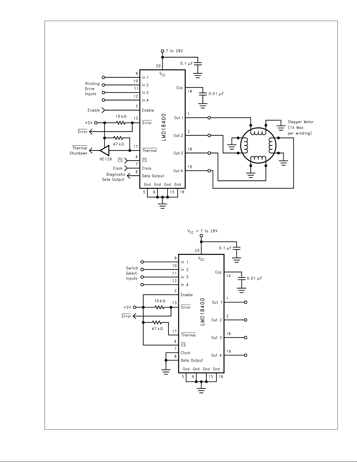
Applications Information (Continued)
LMD18400
Unipolar Drive for a 4-Phase Stepper Motor
01102626
Recommended Connection If No Diagnostics are Required
www.national.com 16
01102627

Applications Information (Continued)
Simple protection of the LMD18400 against supply voltage reversal. Loads will be energized through the intrinsic
diodes in parallel with the power switches. The Schottky diode will add approximately 0.2V to the logic input
switching thresholds and the logic output low levels.
LMD18400
Simple Light “Chaser”
01102628
01102629
www.national.com17

Applications Information (Continued)
LMD18400
Paralleling switches for higher current capability. Positive temperature coefficient of the switch ON resistance
provides ballasting to evenly share the load current between the switches. Any combination of switches can be
paralleled. Required peak load current will depend upon the motor load. Motor speed control can be provided by a
PWM signal of up to 20 kHz applied to the motor drive input lines.
01102630
www.national.com 18

Physical Dimensions inches (millimeters) unless otherwise noted
Order Number LMD18400N
NS Package Number N20A
LMD18400 Quad High Side Driver
LIFE SUPPORT POLICY
NATIONAL’S PRODUCTS ARE NOT AUTHORIZED FOR USE AS CRITICAL COMPONENTS IN LIFE SUPPORT
DEVICES OR SYSTEMS WITHOUT THE EXPRESS WRITTEN APPROVAL OF THE PRESIDENT AND GENERAL
COUNSEL OF NATIONAL SEMICONDUCTOR CORPORATION. As used herein:
1. Life support devices or systems are devices or
systems which, (a) are intended for surgical implant
into the body, or (b) support or sustain life, and
whose failure to perform when properly used in
accordance with instructions for use provided in the
2. A critical component is any component of a life
support device or system whose failure to perform
can be reasonably expected to cause the failure of
the life support device or system, or to affect its
safety or effectiveness.
labeling, can be reasonably expected to result in a
significant injury to the user.
BANNED SUBSTANCE COMPLIANCE
National Semiconductor certifies that the products and packing materials meet the provisions of the Customer Products
Stewardship Specification (CSP-9-111C2) and the Banned Substances and Materials of Interest Specification
(CSP-9-111S2) and contain no ‘‘Banned Substances’’ as defined in CSP-9-111S2.
National Semiconductor
Americas Customer
Support Center
Email: new.feedback@nsc.com
Tel: 1-800-272-9959
www.national.com
National does not assume any responsibility for use of any circuitry described, no circuit patent licenses are implied and National reserves the right at any time without notice to change said circuitry and specifications.
National Semiconductor
Europe Customer Support Center
Fax: +49 (0) 180-530 85 86
Email: europe.support@nsc.com
Deutsch Tel: +49 (0) 69 9508 6208
English Tel: +44 (0) 870 24 0 2171
Français Tel: +33 (0) 1 41 91 8790
National Semiconductor
Asia Pacific Customer
Support Center
Email: ap.support@nsc.com
National Semiconductor
Japan Customer Support Center
Fax: 81-3-5639-7507
Email: jpn.feedback@nsc.com
Tel: 81-3-5639-7560
 Loading...