

National Semiconductor LMC7221 Technical data
July 2002
LMC7221
Tiny CMOS Comparator with Rail-To-Rail Input and Open
Drain Output
General Description
The LM7221 is a micropower CMOS comparator available in
the space saving SOT23-5 package. This makes this comparator ideal for space and weight critical designs. The
LMC7221 is also available in the SO-8 package. The
LMC7221 is supplied in two offset voltage grades, 5 mV and
15 mV.
The open drain output can be pulled up with a resistor to a
voltage which can be higher or lower than the supply
voltage —this makes the part useful for mixed voltage systems.
For a tiny comparator with a push-pull output, please see the
LMC7211 datasheet.
Features
n Tiny SOT 23-5 package saves space
n Package is less than 1.43 mm thick
n Guaranteed specs at 2.7V, 5V, 15V supplies
n Typical supply current 7 µA at 5V
n Response time of 4 µs at 5V
n LMC7221 — open drain output
n Input common-mode range beyond V− and V+
n Low input current
Applications
n Mixed voltage battery powered products
n Notebooks and PDAs
n PCMCIA cards
n Mobile communications
n Alarm and security circuits
n Driving low current LEDs
n Direct sensor interface
LMC7221 Tiny CMOS Comparator with Rail-To-Rail Input and Open Drain Output
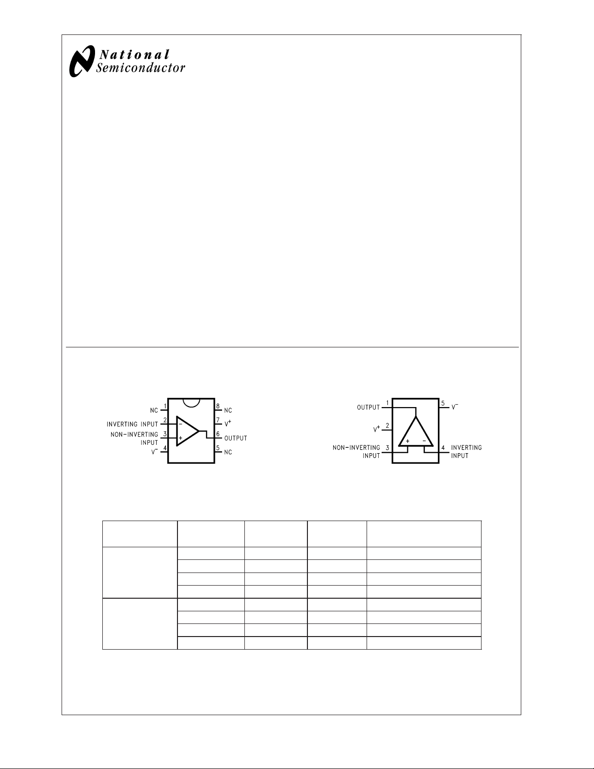
Connection Diagrams
8–Pin SO-8
Top View
Ordering Information
Package Ordering NSC Drawing Package Transport Media
Information Number Marking
LMC7221AIM M08A LMC7221AIM Rails
8-Pin SO-8
5-Pin SOT 23-5
LMC7221AIMX M08A LMC7221AIM 2.5k Units Tape and Reel
LMC7221BIM M08A LMC7221BIM Rails
LMC7221BIMX M08A LMC7221BIM 2.5k Units Tape and Reel
LMC7221AIM5 MA05A C01A 1k Units Tape and Reel
LMC7221AIM5X MA05A C01A 3k Units Tape and Reel
LMC7221BIM5 MA05A C01B 1k Units Tape and Reel
LMC7221BIM5X MA05A C01B 3k Units Tape and Reel
01234601
5-Pin SOT23-5
01234602
Top View
© 2004 National Semiconductor Corporation DS012346 www.national.com
Absolute Maximum Ratings (Note 1)
If Military/Aerospace specified devices are required,
please contact the National Semiconductor Sales Office/
LMC7221
Distributors for availability and specifications.
(soldering, 10 sec.) 260˚C
Storage Temperature Range −65˚C to +150˚C
Junction Temperature
(Note 4) 150˚C
ESD Tolerance (Note 2) 2 kV
Differential Input Voltage (V
Voltage at Input (V
Voltage at Output Pin 15V
Supply Voltage (V
+–V−
) 16V
Current at Input Pin
(Note 7)
Current at Output Pin
(Notes 3, 8)
Current at Power Supply Pin 40 mA
) +0.3V to
CC
(−V
CC
) + 0.3V to
CC
(−V
CC
±
)−0.3V
)−0.3V
±
5mA
30 mA
Operating Ratings (Note 1)
Supply Voltage 2.7 ≤ V
Junction Temperature Range
LMC7221AI, LMC7221BI −40˚C ≤ T
Thermal Resistance (θ
SO-8 Package,
8-Pin Surface Mount 180˚C/W
M05A Package,
5-Pin Surface Mount 325˚C/W
)
JA
Lead Temperature
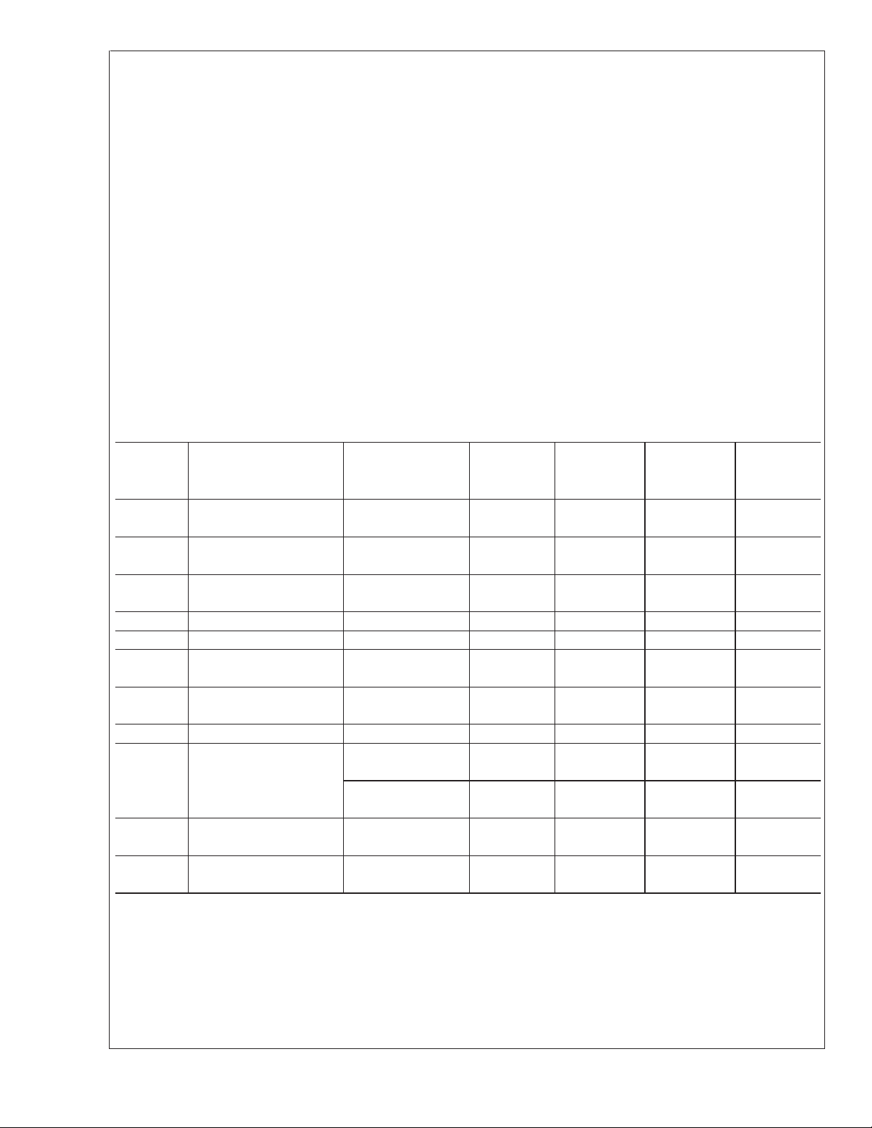
2.7V Electrical Characteristics
Unless otherwise specified, all limits guaranteed for TJ= 25˚C, V+= 2.7V, V−= 0V, VCM=VO= V+/2. Boldface limits apply at
the temperature extremes
Typ LMC7221AI LMC7221BI
Symbol Parameter Conditions (Note 5) Limit Limit Units
(Note 6) (Note 6)
V
OS
TCV
OS
I
B
I
OS
CMRR Common Mode 0V ≤ V
PSRR Power Supply 2.7V ≤ V
A
V
CMVR Input Common-Mode CMRR
V
OL
I
S
Input Offset Voltage 3 5 15 mV
818max
Input Offset Voltage 1.0 µV/˚C
Temperature Drift
Input Offset Voltage (Note 10) 3.3 µV/Month
Average Drift
Input Current 0.04 pA
Input Offset Current 0.02 pA
≤ 2.7V 75 dB
CM
Rejection Ratio
+
≤ 15V 80 dB
Rejection Ratio
Voltage Gain 100 dB
>
55 dB 3.0 2.9 2.9 V
Voltage Range 2.7 2.7 min
>
CMRR
55 dB −0.3 −0.2 −0.2 V
0.0 0.0 max
Output Voltage Low I
= 2.5 mA 0.2 0.3 0.3 V
load
0.4 0.4 max
Supply Current V
= low 7 12 12 µA
OUT
14 14 max
CC
≤ 15V
J
+85˚C
≤
www.national.com 2
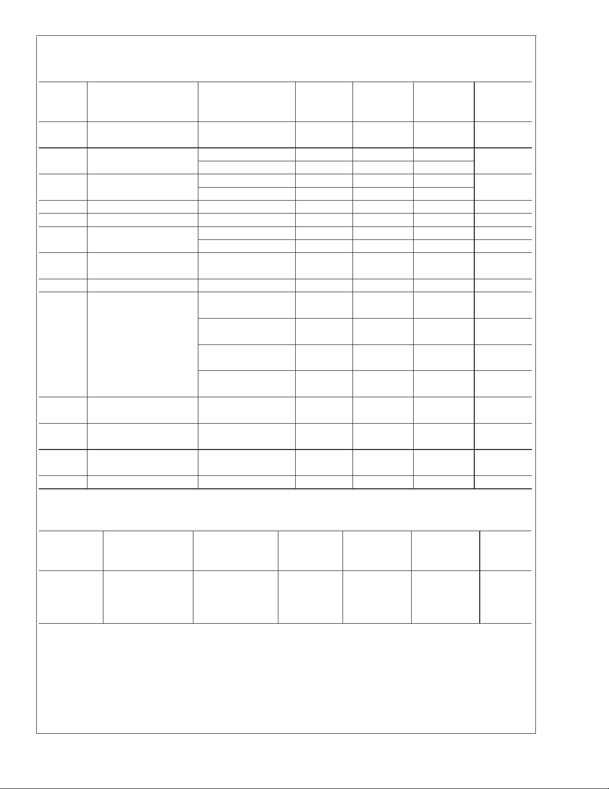
5.0V and 15.0V Electrical Characteristics
Unless otherwise specified, all limits guaranteed for TJ= 25˚C, V+= 5.0V and 15V, V−= 0V, VCM=VO=V+/2. Boldface limits
apply at the temperature extremes
Typ LMC7221AI LMC7221BI
Symbol Parameter Conditions (Note 5) Limit Limit Units
(Note 6) (Note 6)
V
OS
TCV
OS
I
B
I
OS
CMRR Common Mode V+ = 5.0V 75 dB
PSRR Power Supply 5V ≤ V
A
V
CMVR Input Common-Mode V+ = 5.0V 5.3 5.2 5.2 V
V
OL
I
S
I
SC
Input Offset Voltage 3 5 15 mV
818max
Input Offset Voltage V+= 5V 1.0 µV/˚C
Temperature Drift V
Input Offset Voltage V
Average Drift V
+
= 15V 4.0
+
= 5V (Note 10) 3.3 µV/Month
+
= 15V (Note 10) 4.0
Input Current 0.04 pA
Input Offset Current 0.02 pA
Rejection Ration V+ = 15.0V 82 dB
+
≤ 10V 80 dB
Rejection Ratio
Voltage Gain 100 dB
Voltage Range CMRR
>
55 dB 5.0 5.0 min
V+ = 5.0V −0.3 −0.2 −0.2 V
>
CMRR
55 dB 0.0 0.0 max
V+ = 15.0V 15.3 15.2 15.2 V
>
CMRR
55 dB 15.0 15.0 min
V+ = 15.0V −0.3 −0.2 −0.2 V
>
CMRR
55 dB 0.0 0.0 max
Output Voltage Low V+ = 5V 0.2 0.40 0.40 mV
I
=5mA 0.55 0.55 max
load
V+ = 15V 0.2 0.40 0.40 mV
I
=5mA 0.55 0.55 max
load
Supply Current V
= Low 7 14 14 µA
OUT
18 18 max
Short Circuit Current Sinking (Note 8) 45 mA
LMC7221
Leakage Characteristics
TJ= 25˚C
Typ LMC7221AI LMC7221BI
Symbol Parameter Conditions (Note 5) Limit Limit Units
(Note 6) (Note 6)
I
LEAKAGE
Output Leakage V+ = 2.7V
Current V
(+) = 0.5V 0.1 500 500 nA
IN
V
(−)=0V
IN
V
= 15V
OUT
www.national.com3

AC Electrical Characteristics
Unless otherwise specified, all limits guaranteed for TJ= 25˚C, V+= 5V, V−= 0V, VCM=VO=V+/2. Boldface limits apply at
the temperature extreme
LMC7221
Typ LMC7221AI LMC7221BI
Symbol Parameter Conditions (Note 5) Limit Limit Units
(Note 6) (Note 6)
t
rise
t
fall
t
PHL
t
PLH
Note 1: Absolute Maximum Ratings indicate limits beyond which damage to the device may occur. Operating Ratings indicate conditions for which the device is
intended to be functional, but specific performance is not guaranteed. For guaranteed specifications and the test conditions, see the Electrical Characteristics.
Note 2: Human body model, 1.5 kΩ in series with 100 pF.
Note 3: Applies to both single-supply and split-supply operation. Continuous short circuit operation at elevated ambient temperature can result in exceeding the
maximum allowed junction temperature of 150˚C. Output currents in excess of
Note 4: The maximum power dissipation is a function of T
Note 5: P
Note 6: Typical values represent the most likely parametric norm.
Note 7: All limits are guaranteed by testing or statistical analysis.
Note 8: Limiting input pin current is only necessary for input voltages which exceed the absolute maximum input voltage rating.
Note 9: Do not short circuit the output to V+ when V+ is greater than 12V or reliability will be adversely affected.
Note 10: C
Note 11: Input offset voltage average drift is calculated by dividing the accelerated operating life V
case input conditions and includes the first 30 days of drift.
Note 12: Input step voltage for propagation delay measurement is 2V.
Rise Time f = 10 kHz, CL= 50 pF, (Note 9) 0.3 µs
Overdrive = 10 mV, 5 kΩ Pullup
Fall Time f = 10 kHz, CL= 50 pF, (Note 9) 0.3 µs
Overdrive = 10 mV, 5 kΩ Pullup
Propagation Delay f = 10 kHz, 10 mV 10 µs
(High to Low) C
= 50 pF, 100 mV 4
L
(Note 11) 5 kΩ Pullup
(Note 9)
V+ = 2.7V, 10 mV 10 µs
f = 10 kHz,
C
= 50 pF, 100 mV 4
L
5kΩ Pullup
(Note 9)
Propagation Delay f = 10 kHz, 10 mV 6 µs
(Low to High) C
= 50 pF, 100 mV 4
L
(Note 11) 5 kΩ Pullup
(Note 9)
V+ = 2.7V, 10 mV 7 µs
f = 10 kHz,
C
= 50 pF, 100 mV 4
L
5kΩ Pullup
(Note 9)
±
30 mA may adversely affect reliability.
, θJA, and TA. The maximum allowable power dissipation at any ambient temperature is
=(T
D
J(max)−TA
includes the probe and test jig capacitance.
L
)/θJA. All numbers apply for packages soldered directly into a PC board.
J(max)
drift by the equivalent operational time. This represents worst
OS
www.national.com 4
 Loading...