

Page 1
LMC7211
Tiny CMOS Comparator with Rail-to-Rail Input and
Push-Pull Output
LMC7211 Tiny CMOS Comparator with Rail-to-Rail Input and Push-Pull Output
August 2002
General Description
The LMC7211 is a micropower CMOS comparator available
in the space saving SOT23-5 package. This makes the
comparator ideal for space and weight critical designs. The
LMC7211 is supplied in two offset voltage grades, 5 mV and
15 mV.
The main benefits of the Tiny package are most apparent in
small portable electronic devices, such as mobile phones,
pagers, notebook computers, personal digital assistants,
and PCMCIA cards. The rail-to-rail input voltage makes the
LMC7211 a good choice for sensor interfacing, such as light
detector circuits, optical and magnetic sensors, and alarm
and status circuits.
The Tiny Comparator’s outside dimensions (length x width x
height) of 3.05mm x 3.00mm x 1.43mm allow it to fit into tight
spaces on PC boards.
See the LMC7221 for a comparator with an open-drain
output.
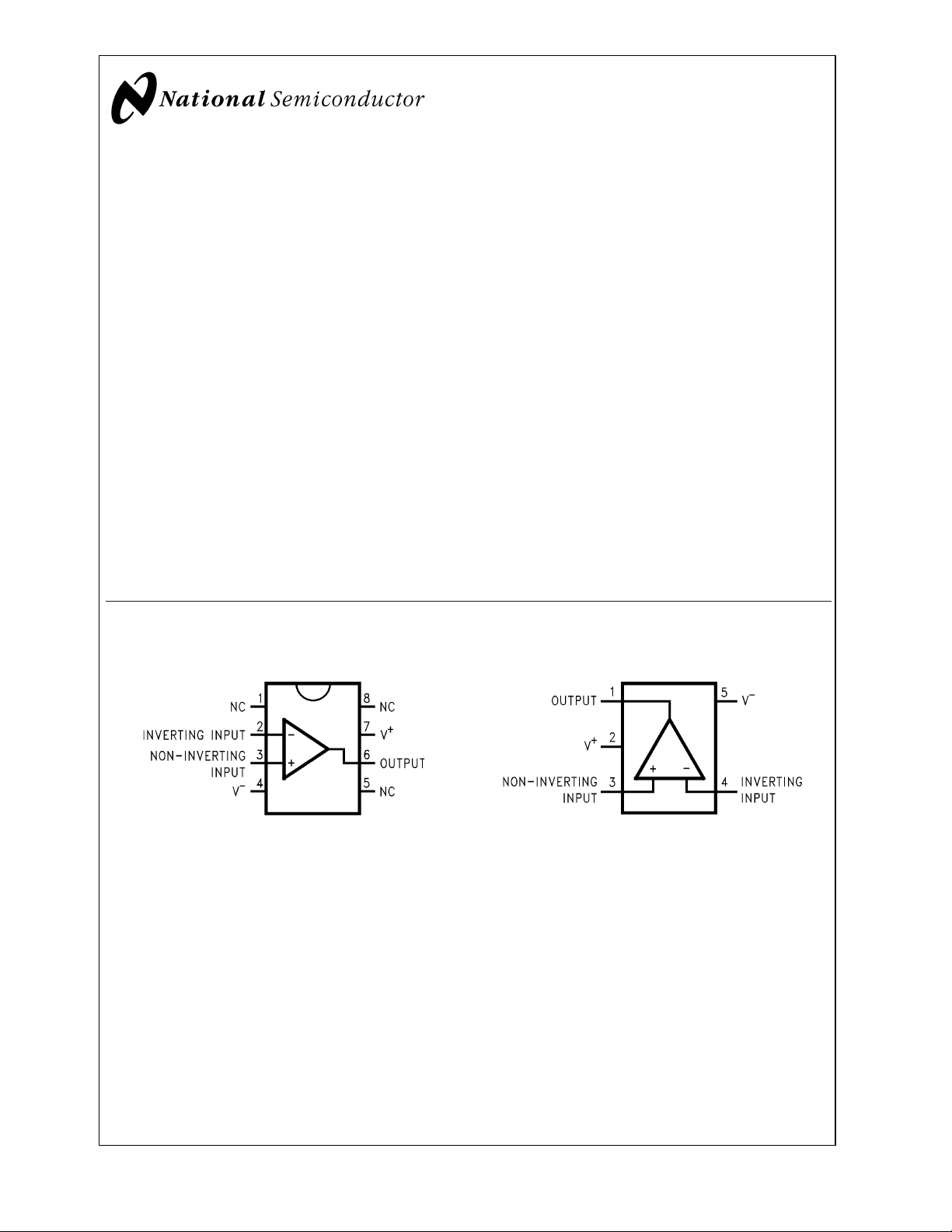
Connection Diagrams
8-Pin SO-8
Features
n Tiny SOT 23-5 package saves space
n Package is less than 1.43 mm thick
n Guaranteed specs at 2.7V, 5V, 15V supplies
n Typical supply current 7 µA at 5V
n Response time of 4 µs at 5V
n Push-pull output
n Input common-mode range beyond V− and V+
n Low input current
Applications
n Battery Powered Products
n Notebooks and PDAs
n PCMCIA cards
n Mobile Communications
n Alarm and Security circuits
n Direct Sensor Interface
n Replaces amplifiers used as comparators with better
performance and lower current
5-Pin SOT23-5
Top View
01233701
© 2002 National Semiconductor Corporation DS012337 www.national.com
Top View
01233702
Page 2
Absolute Maximum Ratings (Note 1)
If Military/Aerospace specified devices are required,
LMC7211
please contact the National Semiconductor Sales Office/
Distributors for availability and specifications.
Storage Temperature
Range −65˚C to +150˚C
Junction Temperature
(Note 4) 150˚C
ESD Tolerance (Note 2) 2 kV
Differential Input Voltage (V
Voltage at Input/Output Pin (V
Supply Voltage (V
+–V−
) 16V
Current at Input Pin (Note
7)
Current at Output Pin
(Notes 3, 8)
Current at Power Supply
Pin 40 mA
) +0.3V to (−VCC)−0.3V
CC
) + 0.3V to
CC
(−V
CC
±
)−0.3V
±
5mA
30 mA
Operating Ratings (Note 1)
Supply Voltage 2.7 ≤ V
Junction Temperature Range
LMC7211AI, LMC7211BI
Thermal Resistance (θJA)
SO-8 Package,
8-Pin Surface Mount 180˚C/W
M05A Package,
5-Pin Surface Mount 325˚C/W
−40˚C ≤ T
Lead Temperature
(soldering, 10 sec) 260˚C
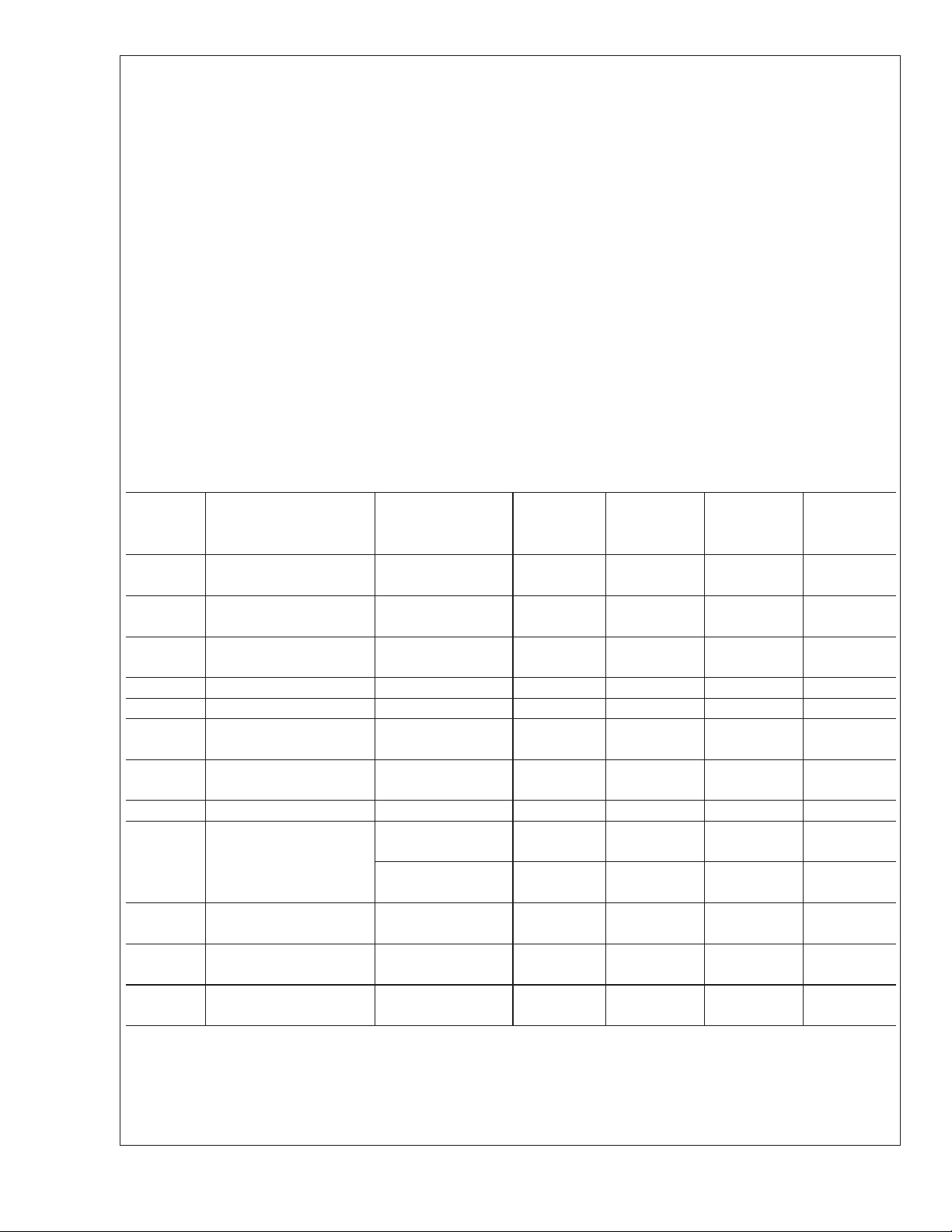
2.7V Electrical Characteristics
Unless otherwise specified, all limits guaranteed for TJ= 25˚C, V+= 2.7V, V−= 0V, VCM=VO= V+/2. Boldface limits apply
at the temperature extremes.
Typ LMC7211AI LMC7211BI
Symbol Parameter Conditions (Note 5) Limit Limit Units
(Note 6) (Note 6)
V
OS
TCV
OS
I
B
I
OS
CMRR Common Mode 0V ≤ V
PSRR Power Supply 2.7V ≤ V
A
V
CMVR Input Common-Mode CMRR
V
OH
V
OL
I
S
Input Offset Voltage 3 5 15 mV
818max
Input Offset Voltage 1.0 µV/˚C
Temperature Drift
Input Offset Voltage (Note 10) 3.3 µV/Month
Average Drift
Input Current 0.04 pA
Input Offset Current 0.02 pA
≤ 2.7V 75 dB
CM
Rejection Ratio
+
≤ 15V 80 dB
Rejection Ratio
Voltage Gain 100 dB
>
55 dB 3.0 2.9 2.9 V
Voltage Range 2.7 2.7 min
>
CMRR
55 dB −0.3 −0.2 −0.2 V
0.0 0.0 max
Output Voltage High I
= 2.5 mA 2.5 2.4 2.4 V
load
2.3 2.3 min
Output Voltage Low I
= 2.5 mA 0.2 0.3 0.3 V
load
0.4 0.4 max
Supply Current V
= Low 7 12 12 µA
OUT
14 14 max
CC
≤ 15V
J
+85˚C
≤
www.national.com 2
Page 3
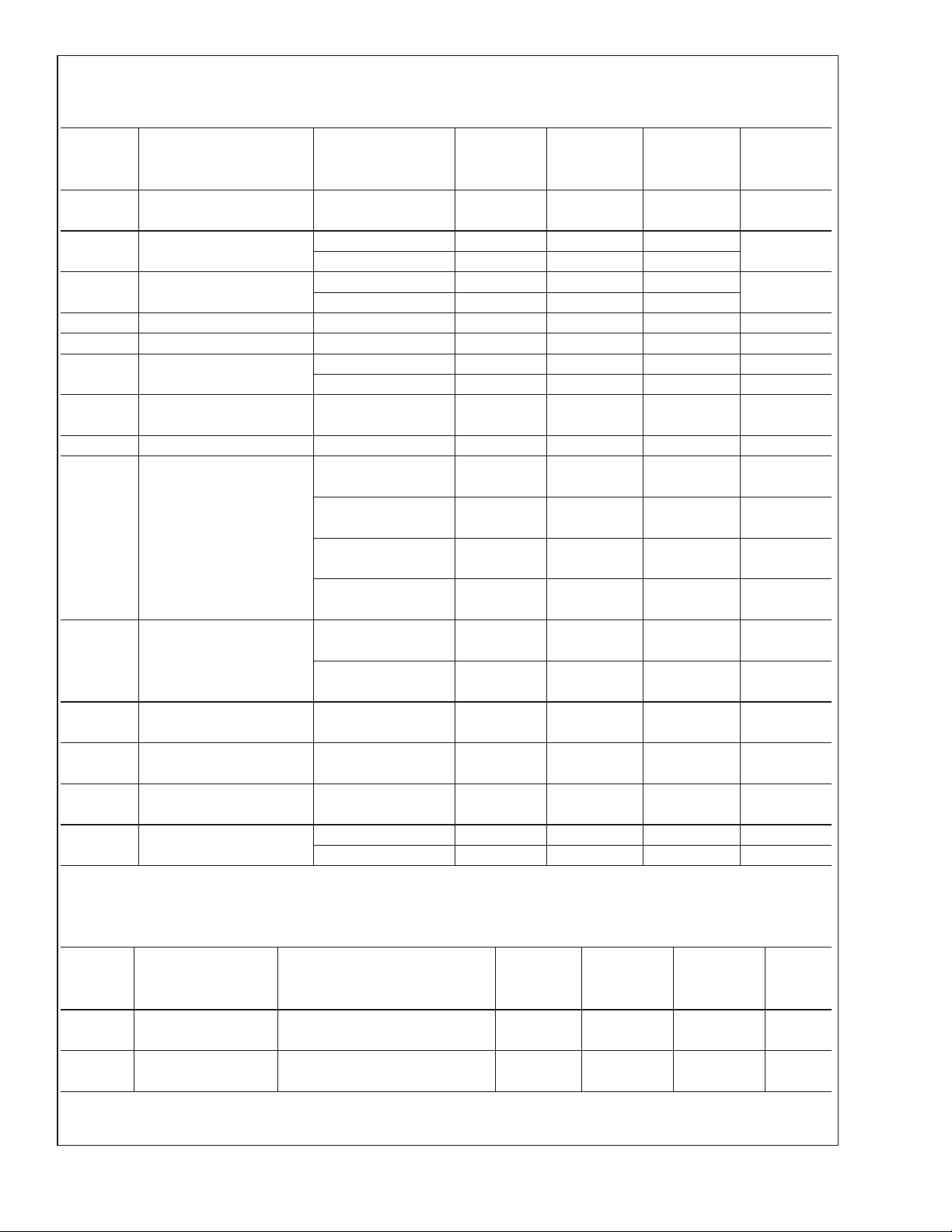
5.0V and 15.0V Electrical Characteristics
Unless otherwise specified, all limits guaranteed for TJ= 25˚C, V+= 5.0V and 15V, V−= 0V, VCM=VO=V+/2. Boldface limits apply at the temperature extremes.
Typ LMC7211AI LMC7211BI
Symbol Parameter Conditions (Note 5) Limit Limit Units
(Note 6) (Note 6)
V
OS
TCV
OS
I
B
I
OS
CMRR Common Mode V+ = 5.0V 75 dB
PSRR Power Supply 5V ≤ V
A
V
CMVR Input Common-Mode V+ = 5.0V 5.3 5.2 5.2 V
V
OH
V
OL
I
S
I
SC
Input Offset Voltage 3 5 15 mV
818max
Input Offset Voltage V+= 5V 1.0 µV/˚C
Temperature Drift V
Input Offset Voltage V
Average Drift V
+
= 15V 4.0
+
= 5V 3.3 µV/Month
+
= 15V 4.0
Input Current 0.04 pA
Input Offset Current 0.02 pA
Rejection Ration V+ = 15.0V 82 dB
+
≤ 10V 80 dB
Rejection Ratio
Voltage Gain 100 dB
Voltage Range CMRR
>
55 dB 5.0 5.0 min
V+ = 5.0V −0.3 −0.2 −0.2 V
>
CMRR
55 dB 0.0 0.0 max
V+ = 15.0V 15.3 15.2 15.2 V
>
CMRR
55 dB 15.0 15.0 min
V+ = 15.0V −0.3 −0.2 −0.2 V
>
CMRR
55 dB 0.0 0.0 max
Output Voltage High V+ = 5V 4.8 4.6 4.6 mV
I
=5mA 4.45 4.45 min
load
V+ = 15V 14.8 14.6 14.6 mV
I
=5mA 14.45 14.45 min
load
Output Voltage Low V+ = 5V 0.2 0.40 0.40 mV
I
=5mA 0.55 0.55 max
load
V+ = 15V 0.2 0.40 0.40 mV
I
=5mA 0.55 0.55 max
load
Supply Current V
= Low 7 14 14 µA
OUT
18 18 max
Short Circuit Current Sourcing 30 mA
Sinking (Note 8) 45 mA
LMC7211
AC Electrical Characteristics
Unless otherwise specified, all limits guaranteed for TJ= 25˚C, V+= 5V, V−= 0V, VCM=VO=V+/2. Boldface limits apply at
the temperature extreme.
Typ LMC7211AI LMC7211BI
Symbol Parameter Conditions (Note 5) Limit Limit Units
(Note 6) (Note 6)
t
rise
t
fall
Rise Time f = 10 kHz, Cl = 50 pF, 0.3 µs
Overdrive = 10 mV (Note 9)
Fall Time f = 10 kHz, Cl = 50 pF, 0.3 µs
Overdrive = 10 mV (Note 9)
www.national.com3
Page 4
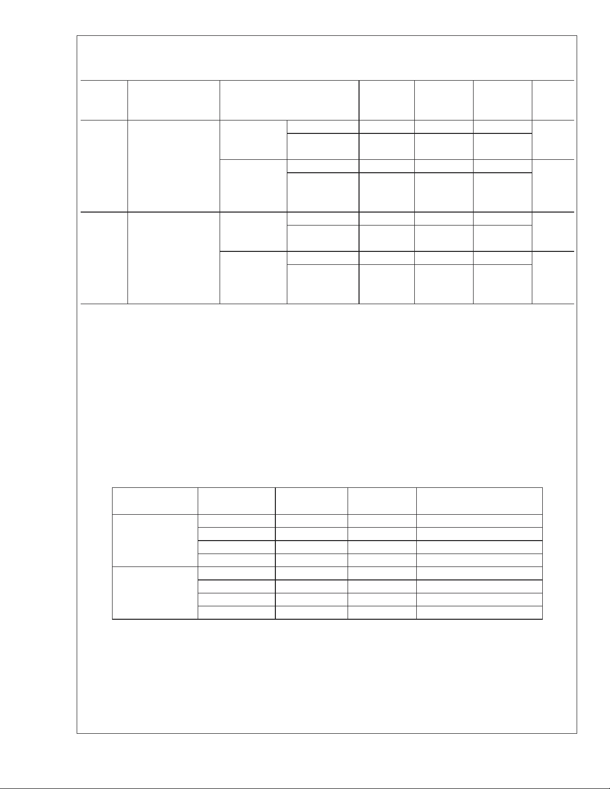
AC Electrical Characteristics (Continued)
Unless otherwise specified, all limits guaranteed for TJ= 25˚C, V+= 5V, V−= 0V, VCM=VO=V+/2. Boldface limits apply at
the temperature extreme.
LMC7211
Typ LMC7211AI LMC7211BI
Symbol Parameter Conditions (Note 5) Limit Limit Units
(Note 6) (Note 6)
t
PHL
t
PLH
Note 1: Absolute Maximum Ratings indicate limits beyond which damage to the device may occur. Operating Ratings indicate conditions for which the device is
intended to be functional, but specific performance is not guaranteed. For guaranteed specifications and the test conditions, see the Electrical Characteristics.
Note 2: Human body model, 1.5 kΩ in series with 100 pF.
Note 3: Applies to both single-supply and split-supply operation. Continuous short circuit operation at elevated ambient temperature can result in exceeding the
maximum allowed junction temperature of 150˚C. Output currents in excess of
Note 4: The maximum power dissipation is a function of T
P
=(T
D
Note 5: Typical values represent the most likely parametric norm.
Note 6: All limits are guaranteed by testing or statistical analysis.
Note 7: Limiting input pin current is only necessary for input voltages that exceed absolute maximum input voltage rating.
Note 8: Do not short circuit output to V+, when V+ is greater than 12V or reliability will be adversely affected.
Note 9: C
Note 10: Input offset voltage average drift is calculated by dividing the accelerated operating life V
case input conditions and includes the first 30 days of drift.
Note 11: Input step voltage for propagation delay measurement is 2V.
Propagation Delay f = 10 kHz, 10 mV 10 µs
(High to Low) Cl = 50 pF 100 mV 4
(Note 11) (Note 9)
V+ = 2.7V, 10 mV 10 µs
f = 10 kHz, 100 mV 4
Cl=50pF
(Note 9)
Propagation Delay f = 10 kHz, 10 mV 6 µs
(Low to High) Cl = 50p 100 mV 4
(Note 11) (Note 9)
V+ = 2.7V, 10 mV 7 µs
f = 10 kHz, 100 mV 4
Cl=50pF
(Note 9)
±
30 mA over long term may adversely affect reliability.
, θJA, and TA. The maximum allowable power dissipation at any ambient temperature is
J(max)−TA
)/θJA.All numbers apply for packages soldered directly into a PC board.
includes the probe and jig capacitance.
L
J(max)
drift by the equivalent operational time. This represents worst
OS
Ordering Information
Package Ordering NSC Drawing Package Transport Media
Information Number Marking
LMC7211AIM M08A LM7211AIM Rails
8-Pin SO-8
5-Pin SOT 23-5
www.national.com 4
LMC7211AIMX M08A LM7211AIM 2.5k Units Tape and Reel
LMC7211BIM M08A LM7211BIM Rails
LMC7211BIMX M08A LM7211BIM 2.5k Units tape and Reel
LMC7211AIM5 MF05A C00A 1k Units Tape and Reel
LMC7211AIM5X MF05A C00A 3k Units Tape and Reel
LMC7211BIM5 MF05A C00B 1k Units Tape and Reel
LMC7211BIM5X MF05A C00B 3k Units Tape and Reel
Page 5

LMC7211
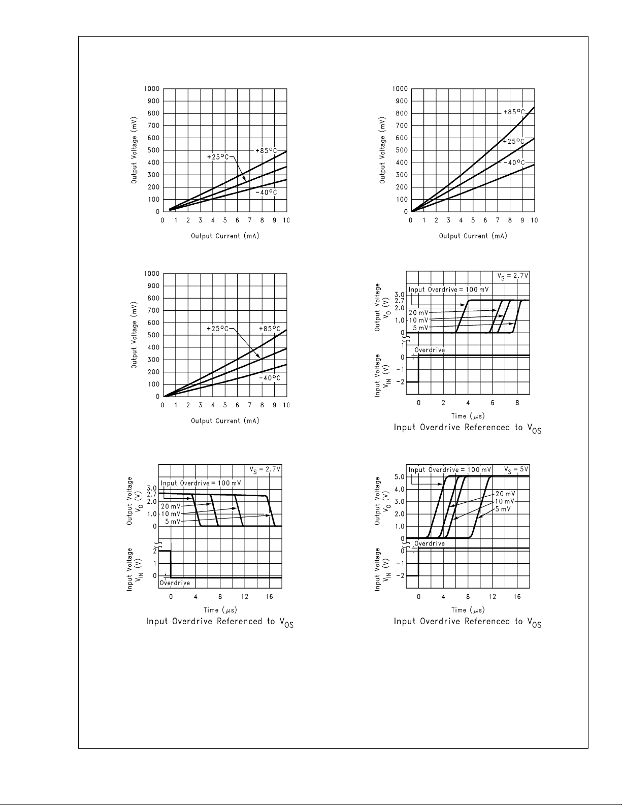
Typical Performance Characteristics Single Supply T
= 25˚C unless specified
A
Supply Current vs. Supply Voltage Supply Current vs. Temperature while Sourcing
01233715 01233716
Supply Current vs. Temperature while Sinking Output Sourcing Current vs. Supply Voltage
01233717
01233718
Output Sinking Current vs. Supply Voltage Output Sinking Current vs. Output Voltage@5V
01233719
01233720
www.national.com5
Page 6
Typical Performance Characteristics Single Supply T
= 25˚C unless specified (Continued)
A
LMC7211
Output Sinking Current vs. Output Voltage
Output Sinking Current vs. Output Voltage@15V Response Time for Various Input Overdrives −t
@
5V Output Sourcing Current vs. Output Voltage@15V
01233721 01233722
PLH
01233723
Response Time for Various Input Overdrives −t
01233725 01233726
PHL
01233724
Response Time for Various Input Overdrives −t
PLH
www.national.com 6
Page 7
LMC7211
Typical Performance Characteristics Single Supply T
Response Time for Various Input Overdrives −t
01233727 01233728
Response Time for Various Input Overdrives −t
PHL
PHL
Response Time for Various Input Overdrives −t
Input Bias Current vs. Common Mode Voltage
= 25˚C unless specified (Continued)
A
PLH
01233730
01233729
Input Bias Current vs. Common Mode Voltage Input Bias Current vs. Common Mode Voltage
01233731
01233732
www.national.com7
Page 8

Typical Performance Characteristics Single Supply T
= 25˚C unless specified (Continued)
A
LMC7211
Input Bias Current vs. Temperature
Application Information
1.0 Benefits of the LMC7211 Tiny Comparator Size. The small footprint of the SOT 23-5 packaged Tiny
Comparator, (0.120 x 0.118 inches, 3.05 x 3.00 mm) saves
space on printed circuit boards, and enable the design of
smaller electronic products. Because they are easier to
carry, many customers prefer smaller and lighter products.
Height. The height (0.056 inches, 1.43 mm) of the Tiny
Comparator makes it possible to use it in PCMCIA type III
cards.
Simplified Board Layout. The Tiny Comparator can simplify board layout in several ways. First, by placing a comparator where comparators are needed, instead of routing
signals to a dual or quad device, long pc traces may be
avoided.
By using multiple Tiny Comparators instead of duals or
quads, complex signal routing and possibly crosstalk can be
reduced.
Low Supply Current. The typical 7 µA supply current of the
LMC7211 extends battery life in portable applications, and
may allow the reduction of the size of batteries in some
applications.
Wide Voltage Range. The LMC7211 is characterized at
15V, 5V and 2.7V. Performance data is provided at these
popular voltages. This wide voltage range makes the
LMC7211 a good choice for devices where the voltage may
vary over the life of the batteries.
Digital Outputs Representing Signal Level. Comparators
provide a high or low digital output depending on the voltage
levels of the (+) and (−) inputs. This makes comparators
useful for interfacing analog signals to microprocessors and
other digital circuits. The LMC7211 can be thought of as a
one-bit a/d converter.
Push-Pull Output. The push-pull output of the LMC7211 is
capable of both sourcing and sinking milliamp level currents
even at a 2.7 volt supply. This can allow the LMC7211 to
drive multiple logic gates.
Driving LEDs (Light Emitting Diodes). With a 5 volt power
supply, the LMC7211’s output sinking current can drive
small, high efficiency LEDs for indicator and test point circuits. The small size of the Tiny package makes it easy to
find space to add this feature to even compact designs.
01233733
Input range to Beyond Rail to Rail. The input common
mode range of the LMC7211 is slightly larger than the actual
power supply range. This wide input range means that the
comparator can be used to sense signals close to the power
supply rails. This wide input range can make design easier
by eliminating voltage dividers, amplifiers, and other front
end circuits previously used to match signals to the limited
input range of earlier comparators. This is useful to power
supply monitoring circuits which need to sense their own
power supply, and compare it to a reference voltage which is
close to the power supply voltage. The wide input range can
also be useful for sensing the voltage drop across a current
sense resistor for battery chargers.
Zero Crossing Detector. Since the LMC7211’s common
mode input range extends below ground even when powered by a single positive supply, it can be used with large
input resistors as a zero crossing detector.
Low Input Currents and High Input Impedance. These
characteristics allow the LMC7211 to be used to sense high
impedance signals from sensors. They also make it possible
to use the LMC7211 in timing circuits built with large value
resistors. This can reduce the power dissipation of timing
circuits. For very long timing circuits, using high value resistors can reduce the size and cost of large value capacitors
for the same R-C time constant.
Direct Sensor Interfacing. The wide input voltage range
and high impedance of the LMC7211 may make it possible
to directly interface to a sensor without the use of amplifiers
or bias circuits. In circuits with sensors which can produce
outputs in the tens to hundreds of millivolts, the LMC7211
can compare the sensor signal with an appropriately small
reference voltage. This may be done close to ground or the
positive supply rail. Direct sensor interfacing may eliminate
the need for an amplifier for the sensor signal. Eliminating
the amplifier can save cost, space, and design time.
2.0 Low Voltage Operation
Comparators are the common devices by which analog signals interface with digital circuits. The LMC7211 has been
designed to operate at supply voltages of 2.7V without sacrificing performance to meet the demands of 3V digital systems.
At supply voltages of 2.7V, the common-mode voltage range
extends 200 mV (guaranteed) below the negative supply.
www.national.com 8
Page 9

Application Information (Continued)
This feature, in addition to the comparator being able to
sense signals near the positive rail, is extremely useful in low
voltage applications.
LMC7211
01233707
FIGURE 3. Measurement of the Shoot-Through Current
01233705
FIGURE 1. Even at Low-Supply Voltage of 2.7V, an
Input Signal which Exceeds the Supply Voltages
Produces No Phase Inversion at the Output
+
= 2.7V propagation delays are t
At V
= 4 µs and t
PLH
PHL
4 µs with overdrives of 100 mV.
Please refer to the performance curves for more extensive
characterization.
3.0 Shoot-Through Current
The shoot-through current is defined as the current surge,
above the quiescent supply current, between the positive
and negative supplies of a device. The current surge occurs
when the output of the device switches states. The
shoot-through current results in glitches in the supply voltages. Usually, glitches in the supply lines are prevented by
bypass capacitors. When the glitches are minimal, the value
of the bypass capacitors can be reduced.
01233706
FIGURE 2. Circuit for Measurement of the
Shoot-Through Current
From Figure 3, the shoot-through current for the LMC7211
can be calculated to be 0.2 mA (typical), and the duration is
1 µs. The values needed for the bypass capacitors can be
calculated as follows:
=
01233708
Area of ∆ =1⁄2(1 µs x 200 µA)
= 100 pC
The capacitor needs to supply 100 picocolumb. To avoid
large shifts in the comparator threshold due to changes in
the voltage level, the voltage drop at the bypass capacitor
should be limited to 100 mV or less.
The charge needed (100 picocolumb) and the allowable
voltage drop (100 mV) will give us the minimum capacitor
value required.
∆Q=C(∆V)
C=∆Q/∆V = 100 picocolumb/100 mV
-10
C=10
10
/10-1=10-9= 1 nF = 0.001 µF
-9
= 1 nF = 0.001 µF
The voltage drop of ∼100 mV will cause a threshold shift in
the comparator. This threshold shift will be reduced by the
power supply rejection ratio, (PSRR). The PSRR which is
applicable here is not the DC value of PSRR (∼80 dB), but a
transient PSRR which will be usually about 20 dB–40 dB,
depending on the circuit and the speed of the transient. This
will result in an effective threshold shift of about 1 mV to
10 mV.
For precision and level sensing circuits, it is generally a good
goal to reduce the voltage delta on the power supply to a
value equal to or less than the hysteresis of the comparator
circuit. If the above circuit was to be used with 50 mV of
hysteresis, it would be reasonable to increase the bypass
capacitor to 0.01 µF to reduce the voltage delta to 10 mV.
Larger values may be useful for obtaining more accurate and
consistent switching.
www.national.com9
Page 10

Application Information (Continued)
Note that the switching current of the comparator can spread
LMC7211
to other parts of the board as noise. The bypass capacitor
reduces this noise. For low noise systems this may be
reason to make the capacitor larger.
For non-precision circuits, such as using a comparator to
determine if a push-button switch is on or off, it is often
cheaper and easier to use a larger value of hysteresis and a
small value or bypass capacitance. The low shoot-through
current of the LMC7211 can allow the use of smaller and less
expensive bypass capacitors in non-critical circuits.
4.0 Output Short Circuit Current
The LMC7211 has short circuit protection of 40 mA. However, it is not designed to withstand continuous short circuits,
transient voltage or current spikes, or shorts to any voltage
beyond the supplies. A resistor in series with the output
should reduce the effect of shorts. For outputs which send
signals off PC boards additional protection devices, such as
diodes to the supply rails, and varistors may be used.
Without Positive Feedback
(No Hysteresis)
01233710
FIGURE 5.
5.0 Hysteresis
If the input signal is very slow or very noisy, the comparator
output might trip several times as the input signal passes
through the threshold. Using positive feedback to add hysteresis to the switching can reduce or eliminate this problem.
The positive feedback can be added by a high value resistor
). This will result in two switching thresholds, one for
(R
F
increasing signals and one for decreasing signals. A capacitor can be added across R
to increase the switching speed
F
and provide more short term hysteresis. This can result in
greater noise immunity for the circuit.
See Figure 4, Figure 5 and Figure 6.
Note that very heavy loading of the comparator output, such
as LED drive or bipolar logic gates, will change the output
voltage and shift the voltage thresholds.
@
R
R1and
F
@
R
R
F
2
01233709
FIGURE 4. Positive Feedback for Hysteresis
With Positive Feedback
(Hysteresis or Memory)
01233711
FIGURE 6.
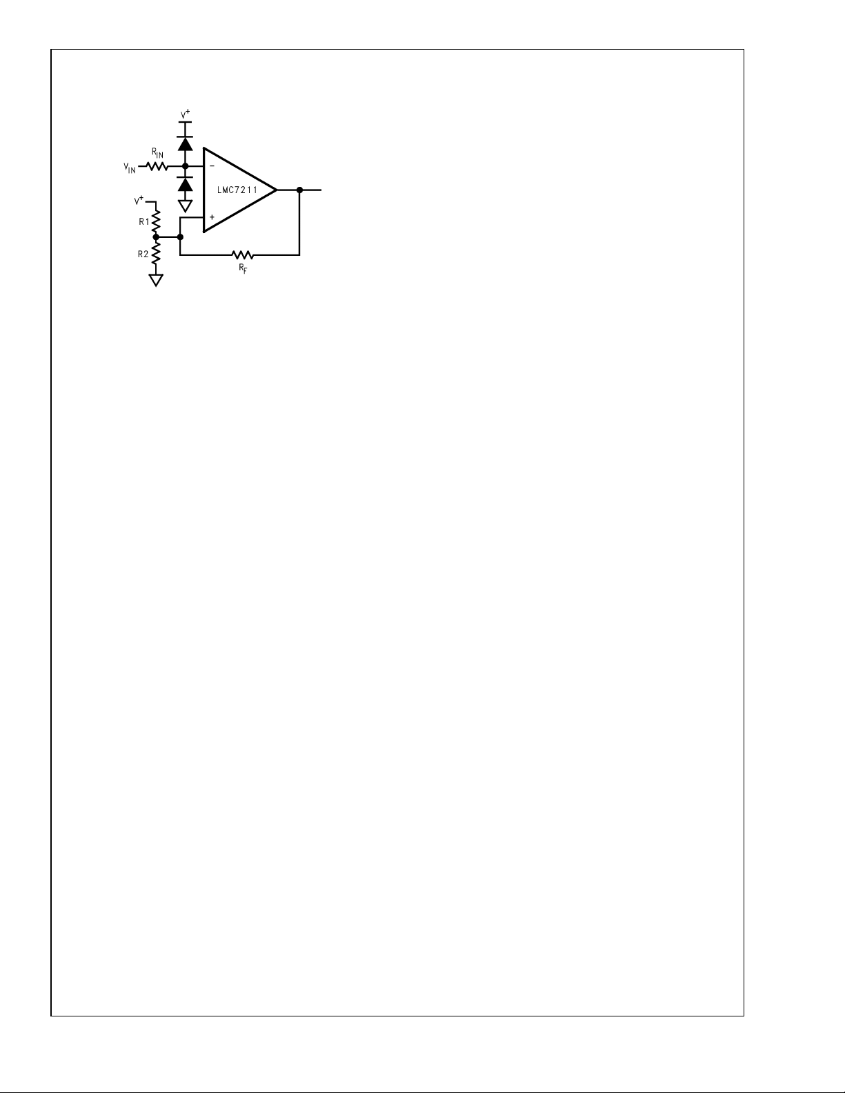
6.0 Input Protection
If input signals are like to exceed the common mode range of
the LMC7211, or it is likely that signals may be present when
power is off, damage to the LMC7211 may occur. Large
value (100 kΩ to MΩ) input resistors may reduce the likelihood of damage by limiting the input currents. Since the
LMC7211 has very low input leakage currents, the effect on
accuracy will be small. Additional protection may require the
use of diodes, as shown in Figure 7. Note that diode leakage
current may affect accuracy during normal operation. The
R-C time constant of R
and the diode capacitance may
IN
also slow response time.
www.national.com 10
Page 11
Application Information (Continued)
01233712
FIGURE 7.
7.0 Layout Considerations
The LMC7211 is not an especially fast comparator, so high
speed design practices are not required. The LMC7211 is
capable of operating with very high impedance inputs, so
precautions should be taken to reduce noise pickup with
high impedance (∼ 100 kΩ and greater) designs and in
electrically noisy environments.
Keeping high value resistors close to the LMC7211 and
minimizing the size of the input nodes is a good practice.
With multilayer designs, try to avoid long loops which could
act as inductors (coils). Sensors which are not close to the
comparator may need twisted pair or shielded connections
to reduce noise.
8.0 Open Drain Output, Dual Versions
The LMC7221 is a comparator similar to the LMC7211, but
with an open drain output which allows the output voltage to
be different (higher or lower) than the supply voltage. The
open drain output is like the open collector output of a logic
gate. This makes the LMC7221 very useful for mixed voltage
systems. Many systems will have different voltages for the
analog and microprocessor sections. Please see the
LMC7221 datasheet for details.
The performance of the LMC7211 is available in dual devices. Please see the LMC6762 datasheet for details on a
dual push-pull output device. For a dual device with open
drain outputs, please see the LMC6772 datasheet.
Rail-to-Rail Input Low Power Comparators —
Push-Pull Output
LMC7211 SOT23-5, SO-8 Single
LMC6762 SO-8, Dual
Open Drain Output
LMC7221 SOT23-5, SO-8 Single
LMC6772 SO-8, DIP Dual
9.0 Additional SOT23-5 Tiny Devices
National Semiconductor has additional parts available in the
space saving SOT23 Tiny package, including amplifiers,
voltage references, and voltage regulators. These devices
include —
LMC7101 1 MHz gain-bandwidth rail-to-rail input and output
amplifier — high input impedance and high gain
700 µA typical current 2.7V, 3V, 5V and 15V
specifications.
LMC7111 Low power 50 kHz gain-bandwidth rail-to-rail in-
put and output amplifier with 25 µA typical current
specified at 2.7V, 3.0V, 3.3V, 5V and 10V.
LM7131 Tiny Video amp with 70 MHz gain bandwidth 3V,
LP2980 Micropower SOT 50 mA Ultra Low-Dropout
LM4040 Precision micropower shunt voltage reference.
LM4041 Precision micropower shut voltage reference
LM385 Low current voltage reference. Fixed Voltages of
Contact your National Semiconductor representative for the
latest information.
10.0 Spice Macromodel
A Spice Macromodel is available for the LMC7211 comparator on the National Semiconductor Amplifier Macromodel
disk. Contact your National Semiconductor representative to
obtain the latest version.
±
5V and
Regulator.
Fixed voltages of 2.500V, 4.096V, 5.000V, 8.192V
and 10.000V.
1.225V and adjustable.
1.2V and 2.5V.
5V specifications.
LMC7211
www.national.com11
Page 12

SOT-23-5 Tape and Reel Specification
LMC7211
REEL DIMENSIONS
8 mm 7.00 0.059 0.512 0.795 2.165 0.331 + 0.059/−0.000 0.567 W1+ 0.078/−0.039
330.00 1.50 13.00 20.20 55.00 8.40 + 1.50/−0.00 14.40 W1 + 2.00/−1.00
Tape Size A B C D N W1 W2 W3
TAPE FORMAT
Tape Section
Leader 0 (min) Empty Sealed
(Start End) 75 (min) Empty Sealed
Carrier 3000 Filled Sealed
Trailer 125 (min) Empty Sealed
(Hub End) 0 (min) Empty Sealed
#
Cavities Cavity Status Cover Tape Status
1000 Filled Sealed
01233713
www.national.com 12
Page 13

SOT-23-5 Tape and Reel Specification (Continued)
Tape Dimensions
LMC7211
8 mm 0.130 0.124 0.130 0.126 0.138±0.002 0.055±0.004 0.157 0.315±0.012
(3.3) (3.15) (3.3) (3.2) (3.5
Tape Size DIM A DIM Ao DIM B DIM Bo DIM F DIM Ko DIM P1 DIM W
±
0.05) (1.4±0.11) (4) (8±0.3)
01233714
www.national.com13
Page 14

Physical Dimensions inches (millimeters) unless otherwise noted
LMC7211
5-Pin SOT Package
NS Package Number MF05A
8-Pin Small Outline Package
NS Package Number M08A
www.national.com 14
Page 15

Notes
LMC7211 Tiny CMOS Comparator with Rail-to-Rail Input and Push-Pull Output
LIFE SUPPORT POLICY
NATIONAL’S PRODUCTS ARE NOT AUTHORIZED FOR USE AS CRITICAL COMPONENTS IN LIFE SUPPORT
DEVICES OR SYSTEMS WITHOUT THE EXPRESS WRITTEN APPROVAL OF THE PRESIDENT AND GENERAL
COUNSEL OF NATIONAL SEMICONDUCTOR CORPORATION. As used herein:
1. Life support devices or systems are devices or
systems which, (a) are intended for surgical implant
into the body, or (b) support or sustain life, and
whose failure to perform when properly used in
accordance with instructions for use provided in the
2. A critical component is any component of a life
support device or system whose failure to perform
can be reasonably expected to cause the failure of
the life support device or system, or to affect its
safety or effectiveness.
labeling, can be reasonably expected to result in a
significant injury to the user.
National Semiconductor
Corporation
Americas
Email: support@nsc.com
www.national.com
National does not assume any responsibility for use of any circuitry described, no circuit patent licenses are implied and National reserves the right at any time without notice to change said circuitry and specifications.
National Semiconductor
Europe
Fax: +49 (0) 180-530 85 86
Email: europe.support@nsc.com
Deutsch Tel: +49 (0) 69 9508 6208
English Tel: +44 (0) 870 24 0 2171
Français Tel: +33 (0) 1 41 91 8790
National Semiconductor
Asia Pacific Customer
Response Group
Tel: 65-2544466
Fax: 65-2504466
Email: ap.support@nsc.com
National Semiconductor
Japan Ltd.
Tel: 81-3-5639-7560
Fax: 81-3-5639-7507
 Loading...