

National Semiconductor LMC6772 Technical data
August 2000
LMC6772
Dual Micropower Rail-To-Rail Input CMOS Comparator
with Open Drain Output
LMC6772 Dual Micropower Rail-To-Rail Input CMOS Comparator with Open Drain Output
General Description
The LMC6772 is an ultra low power dual comparator with a
maximum 10 µA/comparator power supply current. It is designed to operate over a wide range of supply voltages, with
a minimum supply voltage of 2.7V.
The common mode voltage range of the LMC6772 exceeds
both the positive and negative supply rails, a significant advantage in single supply applications. The open drain output
of the LMC6772 allows for wired-OR configurations. The
open drain output also offers the advantage of allowing the
output to be pulled to any voltage rail up to 15V, regardless
of the supply voltage of the LMC6772.
The LMC6772 is targeted for systems where low power consumption is the critical parameter. Guaranteed operation at
supply voltages of 2.7V and rail-to-rail performance makes
this comparator ideal for battery-powered applications.
Refer to the LMC6762 datasheet for a push-pull output stage
version of this device.
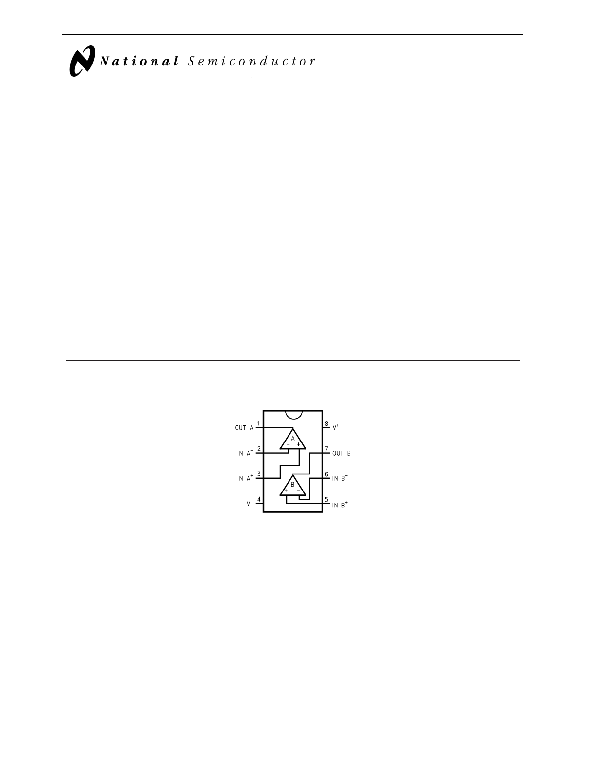
Connection Diagram
8-Pin DIP/SO/MSOP
Features
(Typical unless otherwise noted)
n Low power consumption (max): I
n Wide range of supply voltages: 2.7V to 15V
n Rail-to-Rail Input Common Mode Voltage Range
n Open drain output
n Short circuit protection: 40 mA
n Propagation delay (
@
VS= 5V, 100 mV overdrive): 5 µs
= 10 µA/comp
S
Applications
n Laptop computers
n Mobile phones
n Metering systems
n Hand-held electronics
n RC timers
n Alarm and monitoring circuits
n Window comparators, multivibrators
DS012347-1
Top View
© 2000 National Semiconductor Corporation DS012347 www.national.com
Absolute Maximum Ratings (Note 1)
If Military/Aerospace specified devices are required,
please contact the National Semiconductor Sales Office/
LMC6772
Distributors for availability and specifications.
ESD Tolerance (Note 2) 1.5 kV
Differential Input Voltage (V
Voltage at Input/Output Pin (V
+–V−
Supply Voltage (V
) 16V
Current at Input Pin (Note 8)
Current at Output Pin (Notes 3, 7)
+
)+0.3V to (V−)−0.3V
+
)+0.3V to (V−)−0.3V
±
5mA
±
30 mA
Storage Temperature Range −65˚C to +150˚C
Junction Temperature (Note 4) 150˚C
Operating Ratings (Note 1)
Supply Voltage 2.7 ≤ V
Junction Temperature Range
LMC6772AI, LMC6772BI 40˚C ≤ T
Thermal Resistance (θ
N Package, 8-Pin Molded DIP 100˚C/W
M Package, 8-Pin Surface Mount 172˚C/W
)
JA
Current at Power Supply Pin, LMC6772 40 mA
Lead Temperature (Soldering, 10 seconds) 260˚C
2.7V Electrical Characteristics
Unless otherwise specified, all limits guaranteed for TJ= 25˚C, V+= 2.7V, V−= 0V, VCM=V+/2. Boldface limits apply at the
temperature extremes.
Symbol Parameter Conditions Typ
(Note 5)
V
OS
TCV
OS
Input Offset Voltage 3 5 15 mV
Input Offset Voltage 2.0 µV/˚C
Temperature Drift
Input Offset Voltage (Note 10) 3.3 µV/Month
Average Drift
I
B
I
OS
Input Current 0.02 pA
Input Offset Current 0.01 pA
CMRR Common Mode Rejection Ratio 75 dB
PSRR Power Supply Rejection Ratio
A
V
V
CM
Voltage Gain (By Design) 100 dB
Input Common-Mode CMRR>55 dB 3.0 2.9 2.9 V
±
1.35V<V
<
±
7.5V 80 dB
S
Voltage Range 2.7 2.7 min
−0.3 −0.2 −0.2 V
V
OL
I
S
Output Voltage Low I
= 2.5 mA 0.2 0.3 0.3 V
LOAD
Supply Current For Both Comparators 12 20 20 µA
(Output Low) 25 25 max
I
Leakage
Output Leakage Current VIN(+) = 0.5V, 0.1 500 500 nA
V
(−) = 0V, VO= 15V
IN
LMC6772AI LMC6772BI Units
Limit Limit
(Note 6) (Note 6)
818max
0.0 0.0 max
0.4 0.4 max
≤ 15V
S
≤ +85˚C
J
5.0V and 15.0V Electrical Characteristics
Unless otherwise specified, all limits guaranteed for TJ= 25˚C, V+= 5.0V and 15.0V, V−= 0V, VCM=V+/2. Boldface limits
apply at the temperature extremes.
Symbol Parameter Conditions Typ
(Note 5)
V
OS
TCV
www.national.com 2
Input Offset Voltage 3 5 15 mV
Input Offset Voltage V+= 5V 2.0 µV/˚C
OS
Temperature Drift V
Input Offset Voltage V
Average Drift V
+
= 15V 4.0
+
= 5V (Note 10) 3.3 µV/Month
+
= 15V (Note 10) 4.0
LMC6772AI LMC6772BI Units
Limit Limit
(Note 6) (Note 6)
818max

5.0V and 15.0V Electrical Characteristics (Continued)
Unless otherwise specified, all limits guaranteed for TJ= 25˚C, V+= 5.0V and 15.0V, V−= 0V, VCM=V+/2. Boldface limits
apply at the temperature extremes.
Symbol Parameter Conditions Typ
(Note 5)
I
B
I
OS
CMRR Common Mode V
PSRR Power Supply Rejection Ratio
A
V
V
CM
Input Current V = 5V 0.04 pA
Input Offset Current V+= 5V 0.02 pA
+
=5V 75 dB
Rejection Ratio V
+
= 15V 82 dB
±
2.5V<V
<
±
5V 80 dB
S
Voltage Gain (By Design) 100 dB
Input Common-Mode V+= 5.0V 5.3 5.2 5.2 V
Voltage Range CMRR
>
55 dB 5.0 5.0 min
−0.3 −0.2 −0.2 V
+
V
= 15.0V 15.3 15.2 15.2 V
>
CMRR
55 dB 15.0 15.0 min
−0.3 −0.2 −0.2 V
V
OL
I
S
Output Voltage Low V+= 5V 0.2 0.4 0.4 V
I
=5mA 0.55 0.55 max
LOAD
+
V
= 15V 0.2 0.4 0.4 V
I
=5mA 0.55 0.55 max
LOAD
Supply Current For Both Comparators 12 20 20 µA
(Output Low) 25 25 max
I
SC
Short Circuit Current V+= 15V, Sinking, VO= 12V 45 mA
(Note 7)
LMC6772AI LMC6772BI Units
Limit Limit
(Note 6) (Note 6)
0.0 0.0 max
0.0 0.0 max
LMC6772
AC Electrical Characteristics
Unless otherwise specified, all limits guaranteed for TJ= 25˚C, V+= 5V, V−= 0V, VCM=VO=V+/2. Boldface limits apply at
the temperature extreme.
Symbol Parameter Conditions Typ
(Note 5)
t
RISE
Rise Time f = 10 kHz, CL= 50 pF, 0.3 µs
Overdrive = 10 mV (Note 9)
t
FALL
Fall Time f = 10 kHz, CL= 50 pF, 0.3 µs
Overdrive = 10 mV (Note 9)
t
PHL
Propagation Delay f = 10 kHz, 10 mV 10 µs
(High to Low) C
= 50 pF 100 mV 4 µs
L
(Note 9)
+
V
= 2.7V, 10 mV 10 µs
f = 10 kHz,
C
= 50 pF 100 mV 4 µs
L
(Note 9)
LMC6772AI LMC6772BI Units
Limit Limit
(Note 6) (Note 6)
www.national.com3
AC Electrical Characteristics (Continued)
Unless otherwise specified, all limits guaranteed for TJ= 25˚C, V+= 5V, V−= 0V, VCM=VO=V+/2. Boldface limits apply at
LMC6772
the temperature extreme.
Symbol Parameter Conditions Typ
(Note 5)
t
PLH
Propagation Delay f = 10 kHz, 10 mV 10 µs
(Low to High) C
= 50 pF 100 mV 4 µs
L
(Note 9)
+
V
= 2.7V, 10 mV 8 µs
f = 10 kHz,
C
= 50 pF 100 mV 4 µs
L
(Note 9)
Note 1: Absolute Maximum Ratings indicate limits beyond which damage to the devicemayoccur. Operating Ratings indicate conditions for which the device is intended to be functional, but specific performance is not guaranteed. For guaranteed specifications and the test conditions, see the electrical characteristics.
Note 2: Human body model, 1.5 kΩ in series with 100 pF. The output pins of the two comparators (pin 1 and pin 7) have an ESD tolerance of 1.5 kV. All other pins
have an ESD tolerance of 2 kV.
Note 3: Applies to both single-supply and split-supply operation. Continuous short circuit operation at elevated ambient temperature can result in exceeding the
maximum allowed junction temperature of 150˚C. Output currents in excess of
Note 4: The maximum power dissipation is a function of T
–TA)/θJA. All numbers apply for packages soldered directly into a PC board.
Note 5: Typical Values represent the most likely parametric norm.
Note 6: All limits are guaranteed by testing or statistical analysis.
Note 7: Do not short circuit output to V
Note 8: Limiting input pin current is only necessary for input voltages that exceed absolute maximum input voltage ratings.
Note 9: C
Note 10: Input offset voltage Average Drift is calculated by dividing the accelerated operating life drift average by the equivalent operational time. The input offset
voltage average drift represents the input offset voltage change at worst-case input conditions.
inlcudes the probe and jig capacitance. The rise time, fall time and propagation delays are measured with a 2V input step.
L
+
, when V+ is>12V or reliability will be adversely affected.
, θJA, and TA. The maximum allowable power dissipation at any ambient temperature is PD=(T
J(max)
±
30 mA over long term may adversely affect reliability.
LMC6772AI LMC6772BI Units
Limit Limit
(Note 6) (Note 6)
J(max)
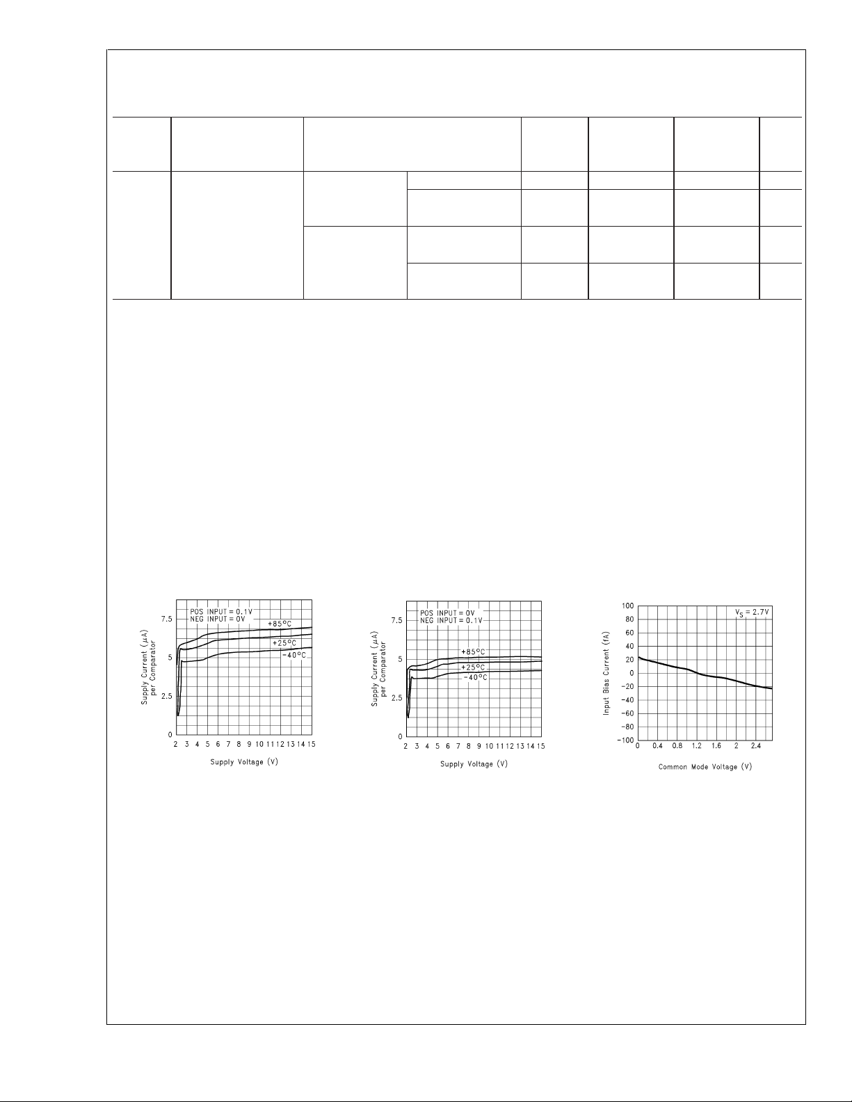
Typical Performance Characteristics V
Supply Current vs Supply
Voltage (Output High)
DS012347-3
Supply Current vs Supply
Voltage (Output Low)
+
= 5V, Single Supply, TA= 25˚C unless otherwise specified
Input Current vs
Common-Mode Voltage
DS012347-4
DS012347-5
www.national.com 4
 Loading...