

查询LMC6484供应商
LMC6484
CMOS Quad Rail-to-Rail Input and Output Operational
Amplifier
LMC6484 CMOS Quad Rail-to-Rail Input and Output Operational Amplifier
May 1999
General Description
The LMC6484 provides a common-mode range that extends
to both supply rails. This rail-to-rail performance combined
with excellent accuracy, due to a high CMRR, makes it
unique among rail-to-rail input amplifiers.
It is ideal for systems, such as data acquisition, that require
a large input signal range. The LMC6484 is also anexcellent
upgrade for circuits using limited common-mode range amplifiers such as the TLC274 and TLC279.
Maximum dynamic signal range is assured in low voltage
and single supply systems by the LMC6484’s rail-to-rail output swing.TheLMC6484’srail-to-railoutput swing is guaranteed for loads down to 600Ω.
Guaranteed low voltage characteristics and low power dissipation make the LMC6484 especially well-suited for
battery-operated systems.
See the LMC6482 data sheet for a Dual CMOS operational
amplifier with these same features.
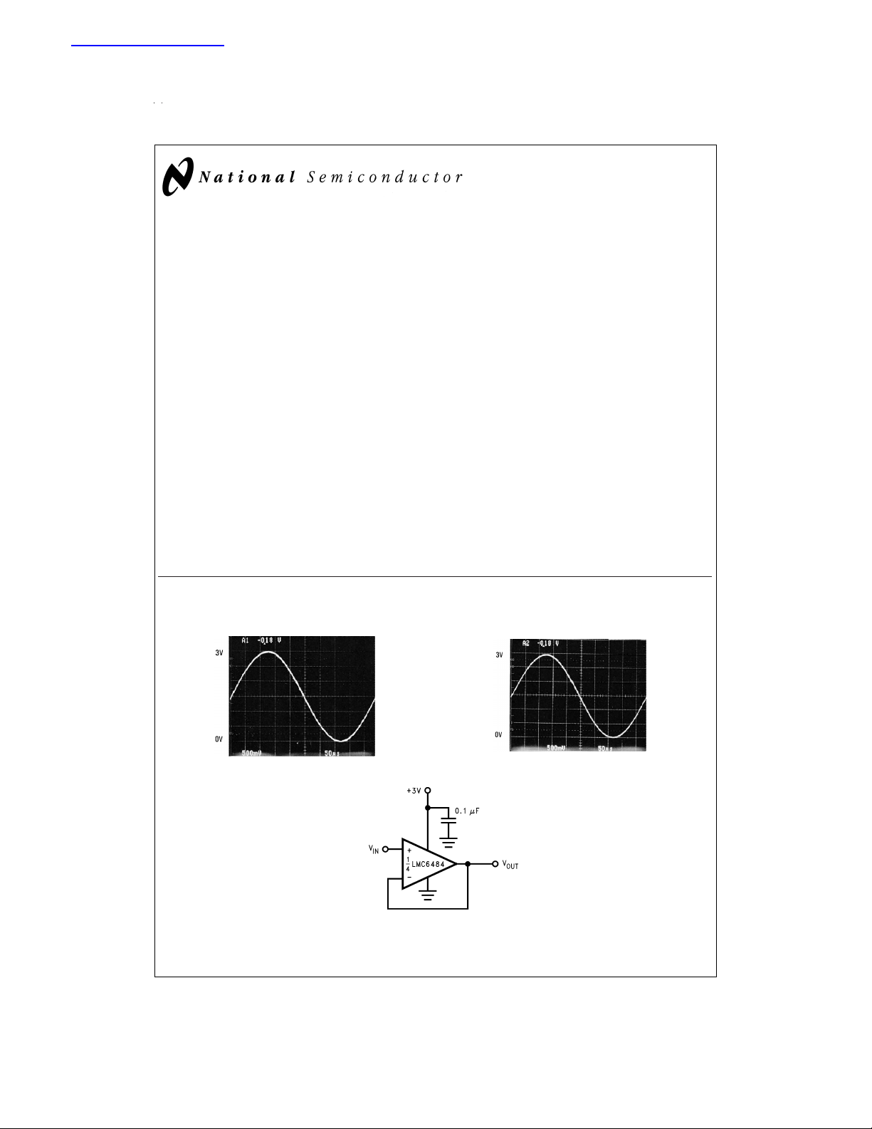
3V Single Supply Buffer Circuit
Rail-to-Rail Input
Features
(Typical unless otherwise noted)
n Rail-to-Rail Input Common-Mode Voltage Range
(Guaranteed Over Temperature)
n Rail-to-Rail Output Swing (within 20 mV of supply rail,
100 kΩ load)
n Guaranteed 3V, 5V and 15V Performance
n Excellent CMRR and PSRR: 82 dB
n Ultra Low Input Current: 20 fA
n High Voltage Gain (R
n Specified for 2 kΩ and 600Ω loads
=
500 kΩ): 130 dB
L
Applications
n Data Acquisition Systems
n Transducer Amplifiers
n Hand-held Analytic Instruments
n Medical Instrumentation
n Active Filter, Peak Detector, Sample and Hold, pH
Meter, Current Source
n Improved Replacement for TLC274, TLC279
Rail-to-Rail Output
DS011714-1
DS011714-2
© 1999 National Semiconductor Corporation DS011714 www.national.com
DS011714-3
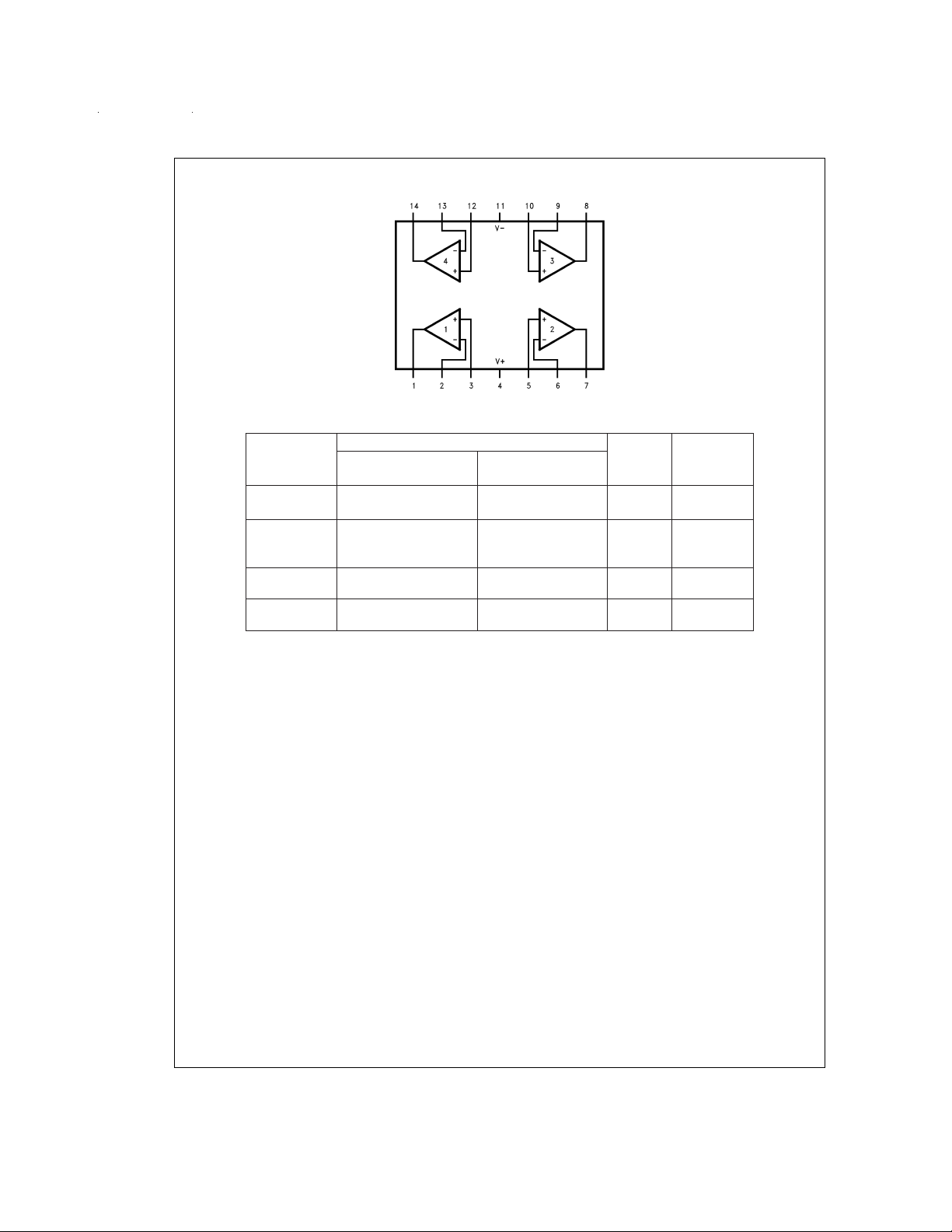
Connection Diagram
Ordering Information
Package Temperature Range NSC
14-pin LMC6484MN LMC6484AIN N14A Rail
Molded DIP LMC6484IN
14-pin LMC6484AIM M14A Rail
Small Outline LMC6484IM Tape and
14-pin Ceramic
DIP
14-pin
Ceramic SOIC
DS011714-4
Military Industrial
−55˚C to +125˚C −40˚C to +85˚C
LMC6484AMJ/883 J14A Rail
LMC6484AMWG/883 WG14A Tray
Drawing
Transport
Media
Reel
www.national.com 2
Absolute Maximum Ratings (Note 1)
If Military/Aerospace specified devices are required,
please contact the National Semiconductor Sales Office/
Distributors for availability and specifications.
ESD Tolerance (Note 2) 2.0 kV
Differential Input Voltage
Voltage at Input/Output Pin (V
Supply Voltage (V
+−V−
) 16V
Current at Input Pin (Note 12)
Current at Output Pin
(Notes 3, 8)
Current at Power Supply Pin 40 mA
Lead Temp. (Soldering, 10 sec.) 260˚C
±
Supply Voltage
+
) + 0.3V, (V−) − 0.3V
±
5mA
±
30 mA
Storage Temperature Range −65˚C to +150˚C
Junction Temperature (Note 4) 150˚C
Operating Ratings (Note 1)
Supply Voltage 3.0V ≤ V
Junction Temperature Range
LMC6484AM −55˚C ≤ T
LMC6484AI, LMC6484I −40˚C ≤ T
Thermal Resistance (θ
)
JA
N Package, 14-Pin Molded DIP 70˚C/W
M Package, 14-Pin
Surface Mount 110˚C/W
+
≤ 15.5V
≤ +125˚C
J
≤ +85˚C
J
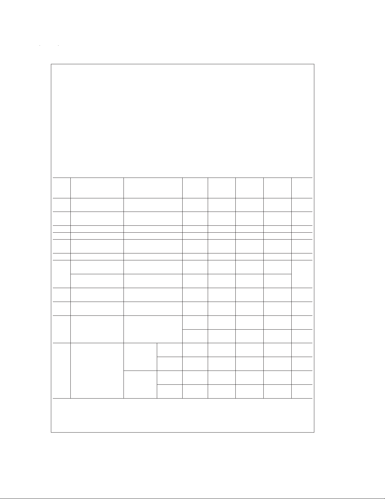
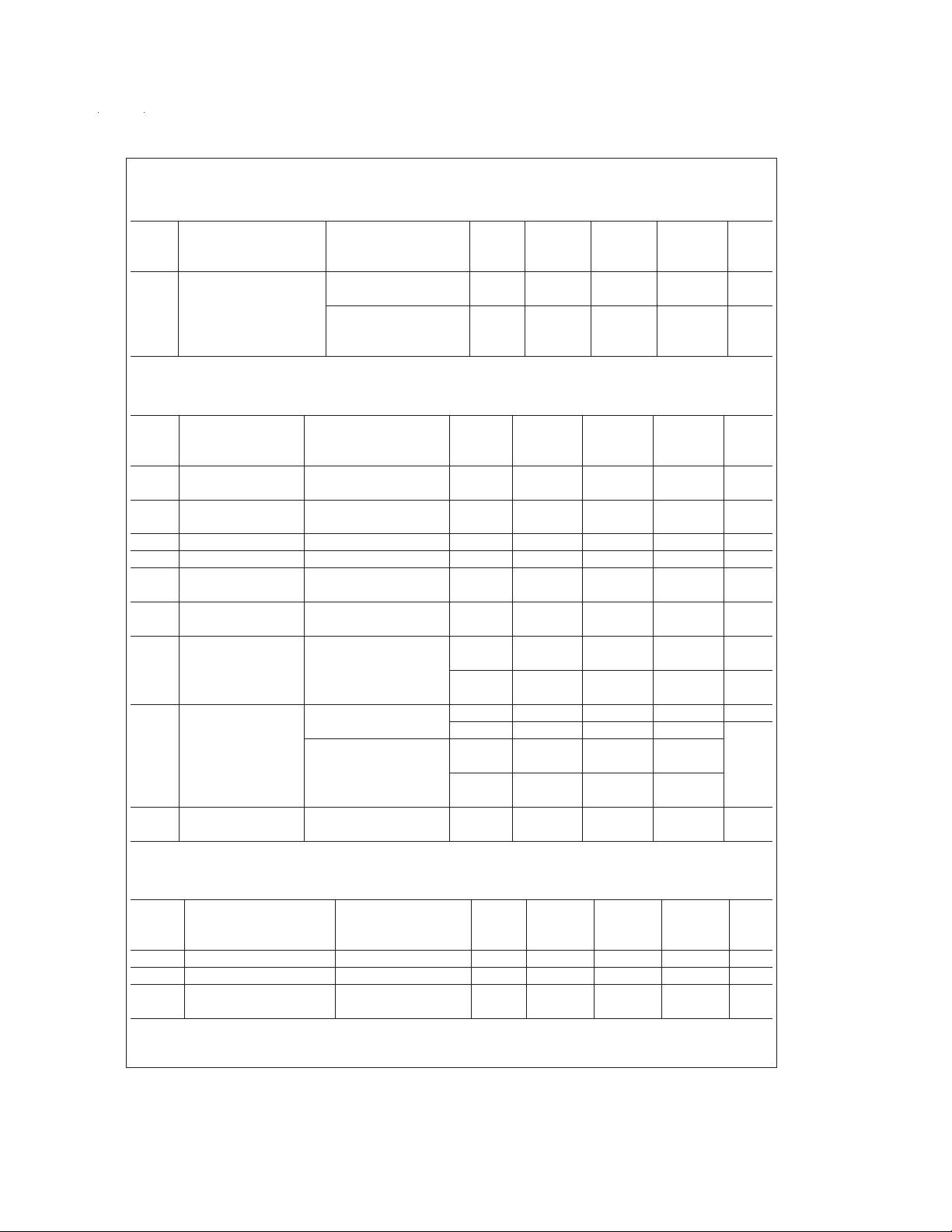
DC Electrical Characteristics
Unless otherwise specified, all limits guaranteed for T
limits apply at the temperature extremes.
=
J
25˚C, V
+
=
5V, V
−
=
0V, V
CM
+
=
=
/2 and R
V
V
O
>
1M. Boldface
L
Typ LMC6484AI LMC6484I LMC6484M
Symbol Parameter Conditions (Note 5) Limit Limit Limit Units
(Note 6) (Note 6) (Note 6)
V
Input Offset Voltage 0.110 0.750 3.0 3.0 mV
OS
1.35 3.7 3.8 max
TCV
Input Offset Voltage 1.0 µV/˚C
OS
Average Drift
I
I
C
Input Current (Note 13) 0.02 4.0 4.0 100 pA max
B
Input Offset Current (Note 13) 0.01 2.0 2.0 50 pA max
OS
Common-Mode 3 pF
IN
Input Capacitance
R
IN
Input Resistance
CMRR Common Mode 0V ≤ V
+
=
Rejection Ratio V
15V 67 62 60
0V ≤ V
+
=
V
5V 67 62 60
+PSRR Positive Power Supply 5V ≤ V
−
Rejection Ratio V
=
0V, V
−PSRR Negative Power Supply −5V ≤ V
+
Rejection Ratio V
V
Input Common-Mode V
CM
=
0V, V
+
=
5V and 15V V
≤ 15.0V, 82 70 65 65 dB
CM
≤ 5.0V 82 70 65 65
CM
+
≤ 15V, 82 70 65 65 dB
=
2.5V 67 62 60 min
O
−
≤ −15V, 82 70 65 65 dB
=
−2.5V 67 62 60 min
O
>
10 Tera Ω
−
− 0.3 −0.25 −0.25 −0.25 V
min
Voltage Range For CMRR ≥ 50 dB 000max
+
V
+ 0.3 V++ 0.25 V++ 0.25 V++ 0.25 V
A
Large Signal R
V
=
2kΩ Sourcing 666 140 120 120 V/mV
L
+
V
+
V
+
V
min
Voltage Gain (Notes 7, 13) 84 72 60 min
Sinking 75 35 35 35 V/mV
20 20 18 min
=
R
600Ω Sourcing 300 80 50 50 V/mV
L
(Notes 7, 13) 48 30 25 min
Sinking 35 20 15 15 V/mV
13 10 8 min
www.national.com3
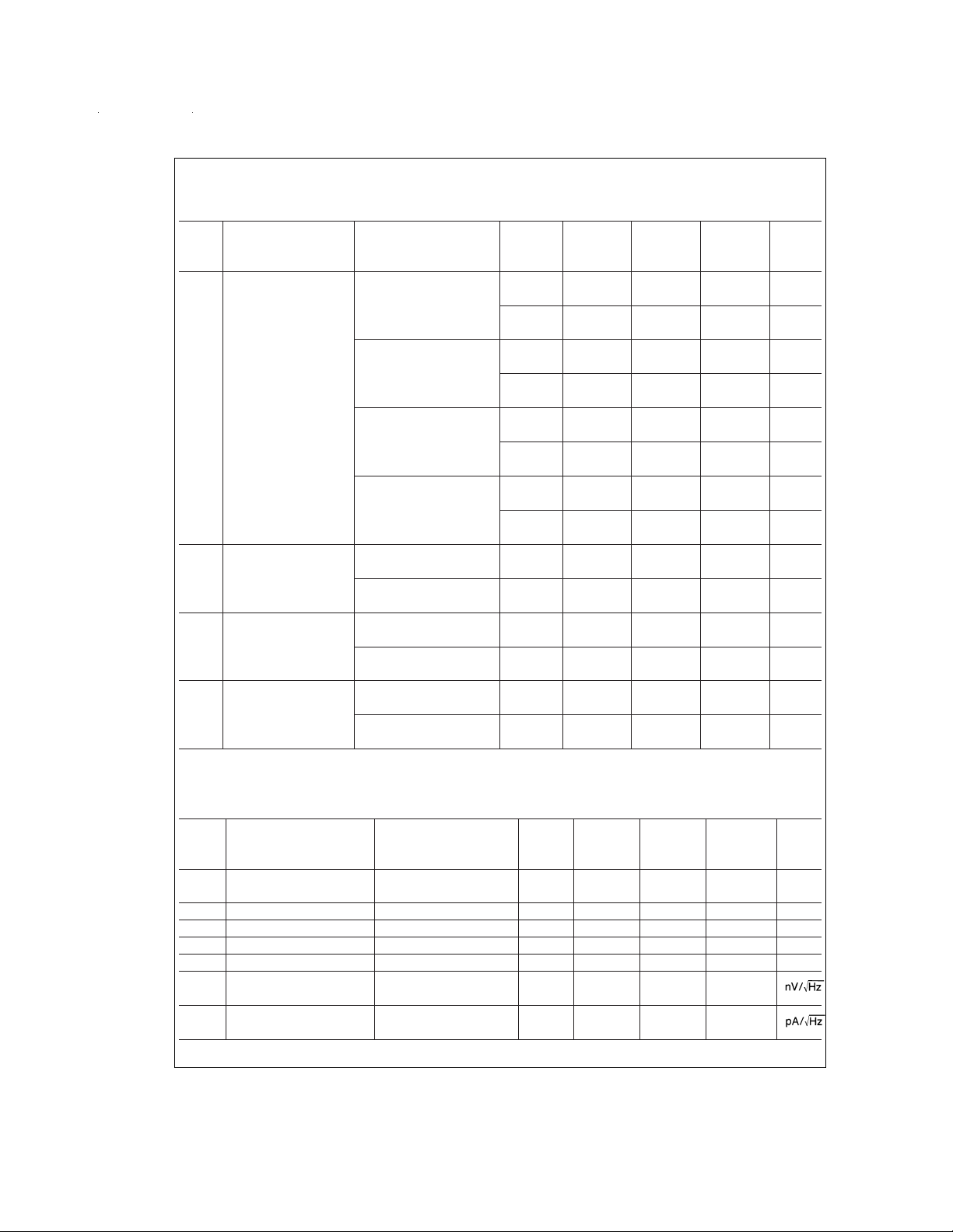
DC Electrical Characteristics (Continued)
Unless otherwise specified, all limits guaranteed for T
limits apply at the temperature extremes.
=
J
25˚C, V
+
Symbol Parameter Conditions (Note 5) Limit Limit Limit Units
+
V
I
Output Swing V
O
Output Short Circuit Sourcing, V
SC
=
5V 4.9 4.8 4.8 4.8 V
=
R
2kΩto V
L
+
=
V
5V 4.7 4.5 4.5 4.5 V
=
R
600Ω to V
L
+
=
V
15V 14.7 14.4 14.4 14.4 V
=
R
2kΩto V
L
+
=
V
15V 14.1 13.4 13.4 13.4 V
=
R
600Ω to V
L
+
/2 4.7 4.7 4.7 min
+
/2 4.24 4.24 4.24 min
+
/2 14.2 14.2 14.2 min
+
/2 13.0 13.0 13.0 min
=
0V 20 16 16 16 mA
O
Current 12 12 10 min
V+=5V Sinking, V
I
Output Short Circuit Sourcing, V
SC
=
5V 15 11 11 11 mA
O
=
0V 30 28 28 28 mA
O
Current 22 22 20 min
+
=
V
15V Sinking, V
=
12V 30 30 30 30 mA
O
(Note 8) 24 24 22 min
I
Supply Current All Four Amplifiers 2.0 2.8 2.8 2.8 mA
S
+
=
V
+5V, V
+
=
/2 3.6 3.6 3.8 max
V
O
All Four Amplifiers 2.6 3.0 3.0 3.0 mA
V
+
=
+15V, V
+
=
/2 3.8 3.8 4.0 max
V
O
=
5V, V
−
=
0V, V
CM
+
=
=
/2 and R
V
V
O
>
1M. Boldface
L
Typ LMC6484AI LMC6484I LMC6484M
(Note 6) (Note 6) (Note 6)
0.1 0.18 0.18 0.18 V
0.24 0.24 0.24 max
0.3 0.5 0.5 0.5 V
0.65 0.65 0.65 max
0.16 0.32 0.32 0.32 V
0.45 0.45 0.45 max
0.5 1.0 1.0 1.0 V
1.3 1.3 1.3 max
9.5 9.5 8.0 min
AC Electrical Characteristics
Unless otherwise specified, all limits guaranteed for T
limits apply at the temperature extremes.
=
J
25˚C, V
+
=
5V, V
−
=
0V, V
CM
+
=
=
/2 and R
V
V
O
>
1M. Boldface
L
Typ LMC6484A LMC6484I LMC6484M
Symbol Parameter Conditions (Note 5) Limit Limit Limit Units
(Note 6) (Note 6) (Note 6)
SR Slew Rate (Note 9) 1.3 1.0 0.9 0.9 V/µs
0.7 0.63 0.54 min
+
=
GBW Gain-Bandwidth Product V
φ
G
Phase Margin 50 Deg
m
Gain Margin 15 dB
m
15V 1.5 MHz
Amp-to-Amp Isolation (Note 10) 150 dB
e
i
n
Input-Referred f=1 kHz 37
n
Voltage Noise V
=
1V
CM
Input-Referred f=1 kHz 0.03
Current Noise
www.national.com 4
AC Electrical Characteristics (Continued)
Unless otherwise specified, all limits guaranteed for T
limits apply at the temperature extremes.
=
J
25˚C, V
+
Symbol Parameter Conditions (Note 5) Limit Limit Limit Units
=
T.H.D. Total Harmonic Distortion f=1 kHz, A
=
R
10 kΩ,V
L
f=10 kHz, A
=
R
10 kΩ,V
L
+
=
V
10V
−2 0.01
V
=
4.1 V
O
V
O
PP
=
−2
=
8.5 V
PP
=
5V, V
−
=
0V, V
CM
+
=
=
/2 and R
V
V
O
L
Typ LMC6484A LMC6484I LMC6484M
(Note 6) (Note 6) (Note 6)
0.01
>
1M. Boldface
%
%
DC Electrical Characteristics
Unless otherwise specified, all limits guaranteed for T
=
J
25˚C, V
+
=
3V, V
−
=
0V, V
CM
+
=
=
/2 and R
V
V
O
>
1M
L
Typ LMC6484AI LMC6484I LMC6484M
Symbol Parameter Conditions (Note 5) Limit Limit Limit Units
(Note 6) (Note 6) (Note 6)
V
Input Offset Voltage 0.9 2.0 3.0 3.0 mV
OS
2.7 3.7 3.8 max
TCV
Input Offset Voltage 2.0 µV/˚C
OS
Average Drift
I
B
I
OS
CMRR Common Mode 0V ≤ V
Input Bias Current 0.02 pA
Input Offset Current 0.01 pA
≤ 3V 74 64 60 60 dB
CM
Rejection Ratio min
PSRR Power Supply 3V ≤ V
+
≤ 15V, V
−
=
0V 80 68 60 60 dB
Rejection Ratio min
V
Input Common-Mode For CMRR ≥ 50 dB V−− 0.25 0 0 0 V
CM
Voltage Range max
+
V
+ 0.25 V
+
+
V
+
V
V
min
V
Output Swing R
O
=
L
2kΩto V
+
/2 2.8 V
0.2 V
R
L
=
600Ω to V
+
/2 2.7 2.5 2.5 2.5 V
min
0.37 0.6 0.6 0.6 V
max
I
S
Supply Current All Four Amplifiers 1.65 2.5 2.5 2.5 mA
3.0 3.0 3.2 max
AC Electrical Characteristics
Unless otherwise specified, V
+
=
3V, V
−
=
0V, V
CM
+
=
=
/2 and R
V
V
O
>
1M
L
Typ LMC6484AI LMC6484I LMC6484M
Symbol Parameter Conditions (Note 5) Limit Limit Limit Units
(Note 6) (Note 6) (Note 6)
SR Slew Rate (Note 11) 0.9 V/µs
GBW Gain-Bandwidth Product 1.0 MHz
=
T.H.D. Total Harmonic Distortion f=10 kHz, A
=
R
10 kΩ,V
Note 1: Absolute Maximum Ratings indicate limits beyond which damage to the device may occur. Operating Ratings indicate conditions for which the device is intended to be functional, but specific performance is not guaranteed. For guaranteed specifications and the test conditions, see the Electrical Characteristics.
Note 2: Human body model, 1.5 kΩ in series with 100 pF. All pins rated per method 3015.6 of MIL-STD-883. This is a class 2 device rating.
L
−2 0.01
V
=
2V
O
PP
%
www.national.com5
AC Electrical Characteristics (Continued)
Note 3: Applies to both single supply and split-supply operation. Continuous short circuit operation at elevated ambient temperature can result in exceeding the maxi-
mum allowed junction temperature of 150˚C. Output currents in excess of
Note 4: The maximum power dissipation is a function of T
−TA)/θJA. All numbers apply for packages soldered directly into a PC board.
Note 5: Typical Values represent the most likely parametric norm.
Note 6: All limits are guaranteed by testing or statistical analysis.
+
Note 7: V
Note 8: Do not short circuit output to V
Note 9: V
Note 10: Input referred, V
Note 11: Connected as Voltage Follower with 2V step input. Number specified is the slower of either the positive or negative slew rates.
Note 12: Limiting input pin current is only necessary for input voltages that exceed absolute maximum input voltage ratings.
Note 13: Guaranteed limits are dictated by tester limitations and not device performance. Actual performance is reflected in the typical value.
Note 14: For guaranteed Military Temperature Range parameters see RETSMC6484X.
=
+
=
=
15V, V
15V. Connected as Voltage Follower with 10V step input. Number specified is the slower of either the positive or negative slew rates.
CM
7.5V and R
+
connected to 7.5V. For Sourcing tests, 7.5V ≤ VO≤ 11.5V. For Sinking tests, 3.5V ≤ VO≤ 7.5V.
L
+
, when V+is greater than 13V or reliability will be adversely affected.
=
15V and R
=
L
J(max)
100 kΩ connected to 7.5V. Each amp excited in turn with 1 kHz to produce V
±
, θJA, and TA. The maximum allowable power dissipation at any ambient temperature is P
30 mA over long term may adversely affect reliability.
=
O
12 V
.
PP
=
(T
D
J(max)
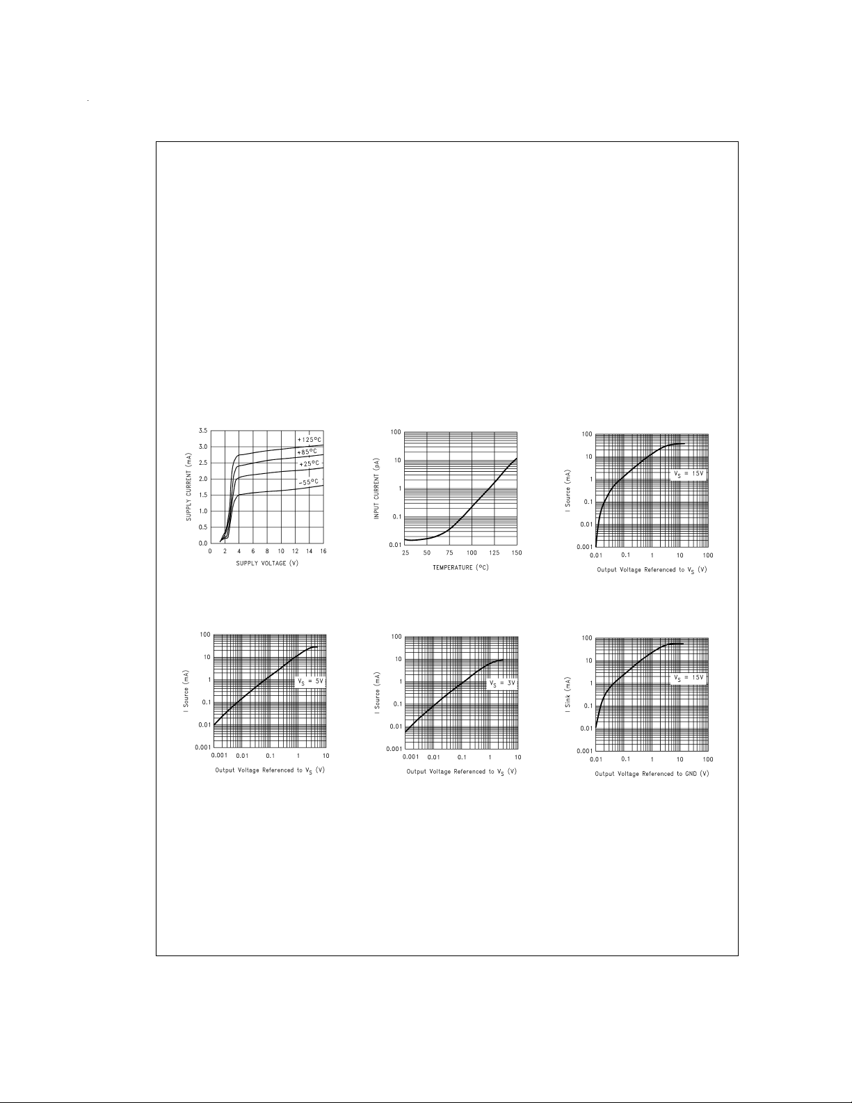
Typical Performance Characteristics V
specified
Supply Current vs
Supply Voltage
DS011714-39
Sourcing Current vs
Output Voltage
Input Current vs
Temperature
Sourcing Current vs
Output Voltage
=
+15V, Single Supply, T
S
DS011714-40
=
25˚C unless otherwise
A
Sourcing Current vs
Output Voltage
Sinking Current vs
Output Voltage
DS011714-41
DS011714-42
www.national.com 6
DS011714-43
DS011714-44
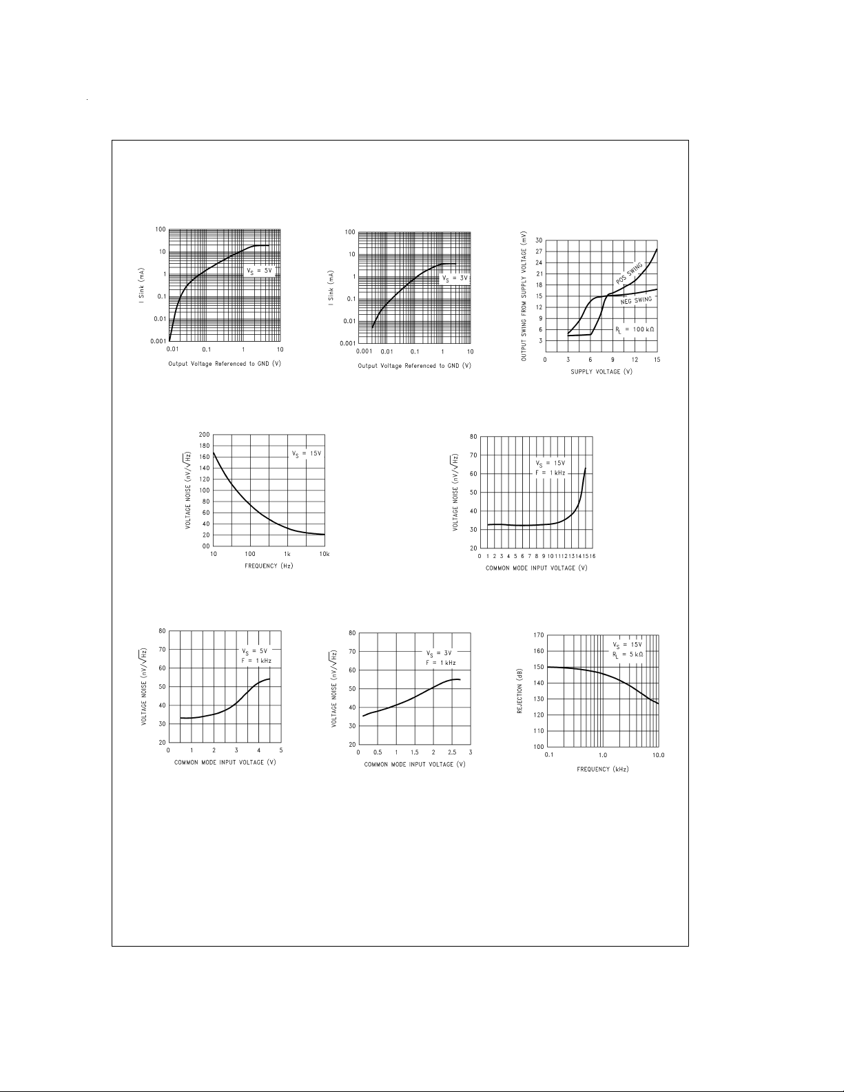
Typical Performance Characteristics V
specified (Continued)
=
+15V, Single Supply, T
S
=
25˚C unless otherwise
A
Sinking Current vs
Output Voltage
Input Voltage Noise
vs Frequency
DS011714-45
Sinking Current vs
Output Voltage
DS011714-48
DS011714-46
Input Voltage Noise
vs Input Voltage
Output Voltage Swing
vs Supply Voltage
DS011714-47
DS011714-49
Input Voltage Noise
vs Input Voltage
DS011714-50
Input Voltage Noise
vs Input Voltage
DS011714-51
Crosstalk Rejection
vs Frequency
DS011714-52
www.national.com7
 Loading...